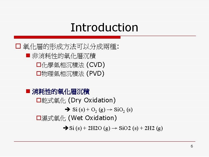
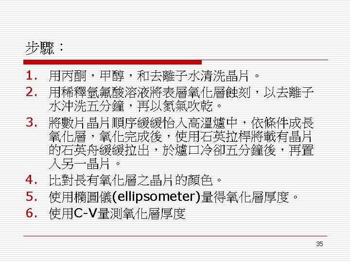
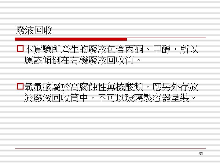
Thermal oxidation of Si and oxide thickness measurement

, Pad Oxide(buffer")


 No Ni o Model: n Ficker’s Law: J=D(No-Ni)/Xo Si. O 2 n Reaction")

 B/A=C 2*exp(-E 2/k. T) Dry C 1 =7. 72 x")
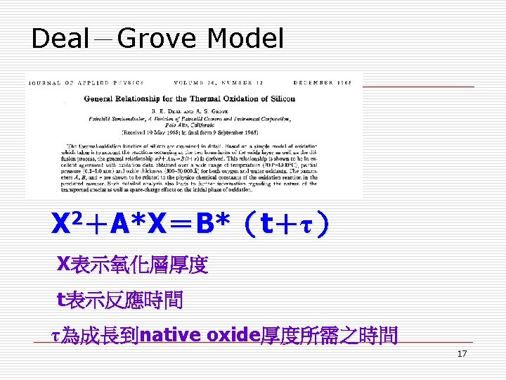
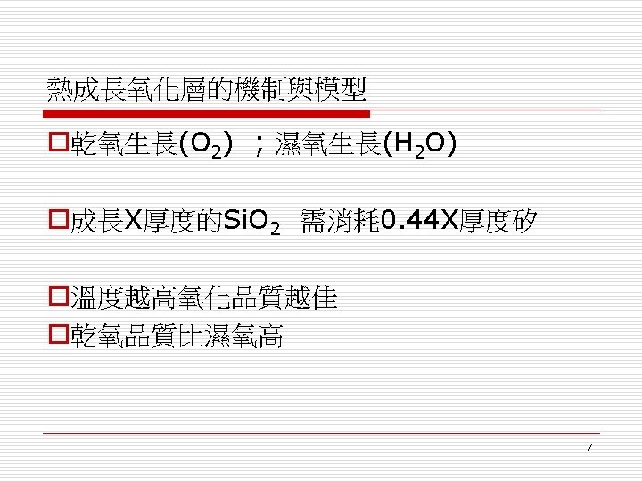
 當t很短時,X很薄,X 2<<A*X,上式趨近 為 A*X=B*(t+τ)/A 此時稱為linear growth regime 或linear rate regime")
 當t很長時,X變厚,X 2>>A*X,上式趨近為 X 2=B*(t+τ) 此時稱為diffusion-limited regime 或parabolic rate regime B稱為Parabolic")
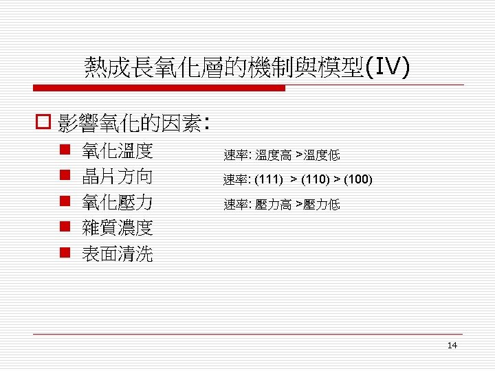
: � (111): � Thus here the molecular density is (110)")
: � (111): � Hence the distance between two layers:")

 >")

 30")
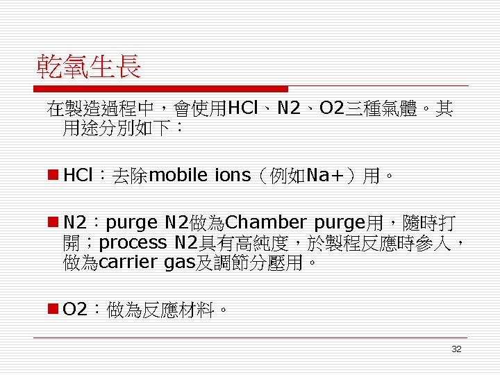
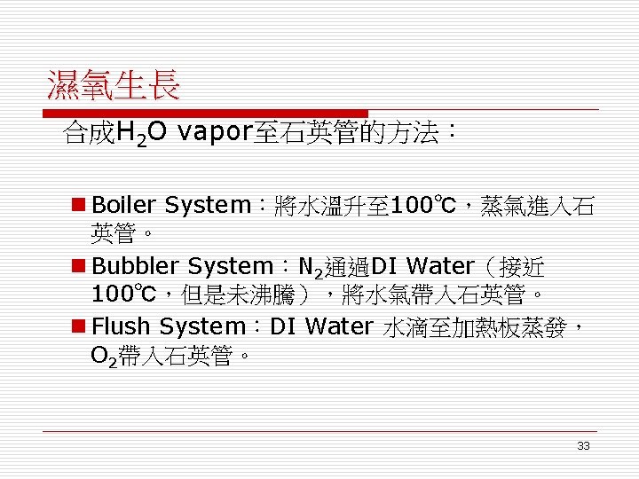
示意圖 Scanning Probe Microscope 34")

- Slides: 40
半導體專題實驗 實驗四 氧化層之成長與厚度量測 Thermal oxidation of Si and oxide thickness measurement 1
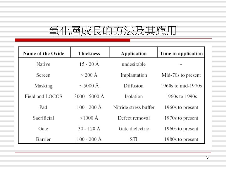
Oxidation in Semiconductor A Typical MOS Profile Screen Oxide (for imp. ), Pad Oxide(buffer oxide, protect active areas) 3 Barrier Oxide, LOCal Oxidation of Silicon
Pad Oxide Bird’s beak effect 4
Color chart of Si. O 2: 9
熱成長氧化層的機制與模型(II) No Ni o Model: n Ficker’s Law: J=D(No-Ni)/Xo Si. O 2 n Reaction rate: J=Ks*Ni Si J=D*No/(D/Ks+Xo) n d. Xo/dt = J/M =(D*No/M) / (Xo+D/Ns) Xo(t)=A/2 ((1+ ( 4 B/A 2 ) *(t+ ) )0. 5 -1) o A=2 D/Ks , B=2 D*No/M o = Xi 2/B + A*Xi/ B n n Xi為一開始氧化層的厚度 X 0可以看成 Xo(t)=B/A (1+ ) 當經過一段長時間後, Xo(t)=(Bt) 1/2 Deal-Grove Model 12
DRY & WET 15
B=C 1*exp(-E 1/k. T) B/A=C 2*exp(-E 2/k. T) Dry C 1 =7. 72 x 102 mm 2 hr-1 E 1 =1. 23 e. V C 2 =6. 23 x 106 mmhr-1 E 2 =2 e. V Wet C 1 =2. 14 x 102 mm 2 hr-1 E 1 =0. 71 e. V C 2 =8. 95 x 107 mmhr-1 E 2 =2. 05 e. V 16
Deal-Grove Model X 2+A*X=B*(t+τ) 當t很短時,X很薄,X 2<<A*X,上式趨近 為 A*X=B*(t+τ)/A 此時稱為linear growth regime 或linear rate regime B/A稱為Linear rate Constant,受控於K(反應速率) 18
Deal-Grove Model X 2+A*X=B*(t+τ) 當t很長時,X變厚,X 2>>A*X,上式趨近為 X 2=B*(t+τ) 此時稱為diffusion-limited regime 或parabolic rate regime B稱為Parabolic rate Constant,受控於D (oxidant在Si. O 2內之擴散速率) 19
Molecular density � (100): � (111): � Thus here the molecular density is (110) > (100) > (111) 20
Distance between layers � (100): � (111): � Hence the distance between two layers: (110) > (111) > (100) � Thus if the oxidation rate on each plane, concerning the molecular density, is not the dominant factor, the rate of thickening the oxide should be fastest for plane (110). 21
Dry oxidation E. A. Irene et al. , Journal of The Electrochemical Society, 133 (6), (1986) Initially, (110) > (111) > (100). Eventually, (111) > (110) > (100). 22
Wet oxidation o Atmospheric pressure, wet oxidation, ~785 degrees Celsius o Initially, (110) > (111) > (100). Eventually, (111) > (110) > (100). 23
Intrinsic Si. O 2 Film Stress Measurements on Thermally Oxidized Si E. Kobeda and E. A. Irene, J. Vac. Sci. Technol. B, 5, 15 ~1987. 24
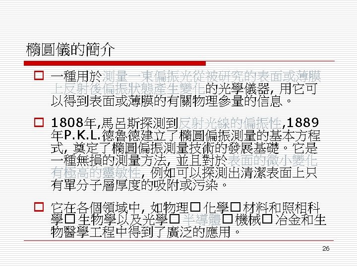
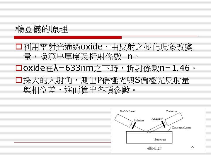
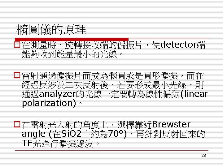
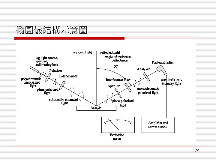
橢圓儀(ellipsometer) 30
表面軌跡分析儀(SPM)示意圖 Scanning Probe Microscope 34
結報問題 1. Find and compare the oxide thickness from the following methods 1. Table 2. Deal-Grove Model 3. Color chart (optical) 4. Ellipsometer (optical) 5. C-V (electrical) 2. Find VFB 3. Find Qox 4. Find Na, Nd 跟過去實驗的濃度做比較 40