The Science and Engineering of Materials 4 th

![Figure 3. 21 Determining the repeat distance, linear density, and packing fraction for [110] Figure 3. 21 Determining the repeat distance, linear density, and packing fraction for [110]](https://slidetodoc.com/presentation_image_h/bc9b6aac5c3f32d5f07dda6cbfdafaca/image-39.jpg)



- Slides: 102

The Science and Engineering of Materials, 4 th ed Donald R. Askeland – Pradeep P. Phulé Chapter 3 – Atomic and Ionic Arrangements 1

Objectives of Chapter 3 o o To learn classification of materials based on atomic/ionic arrangements To describe the arrangements in crystalline solids based on lattice, basis, and crystal structure 2

Chapter Outline o o o o 3. 1 Short-Range Order versus Long-Range Order 3. 2 Amorphous Materials: Principles and Technological Applications 3. 3 Lattice, Unit Cells, Basis, and Crystal Structures 3. 4 Allotropic or Polymorphic Transformations 3. 5 Points, Directions, and Planes in the Unit Cell 3. 6 Interstitial Sites 3. 7 Crystal Structures of Ionic Materials 3. 8 Covalent Structures 3

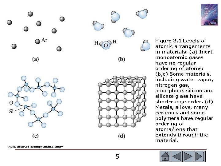
Section 3. 1 Short-Range Order versus Long-Range Order o o o Short-range order - The regular and predictable arrangement of the atoms over a short distance - usually one or two atom spacings. Long-range order (LRO) - A regular repetitive arrangement of atoms in a solid which extends over a very large distance. Bose-Einstein condensate (BEC) - A newly experimentally verified state of a matter in which a group of atoms occupy the same quantum ground state. 4

Figure 3. 1 Levels of atomic arrangements in materials: (a) Inert monoatomic gases have no regular ordering of atoms: (b, c) Some materials, including water vapor, nitrogen gas, amorphous silicon and silicate glass have short-range order. (d) Metals, alloys, many ceramics and some polymers have regular ordering of atoms/ions that extends through the material. (c) 2003 Brooks/Cole Publishing / Thomson Learning™ 5

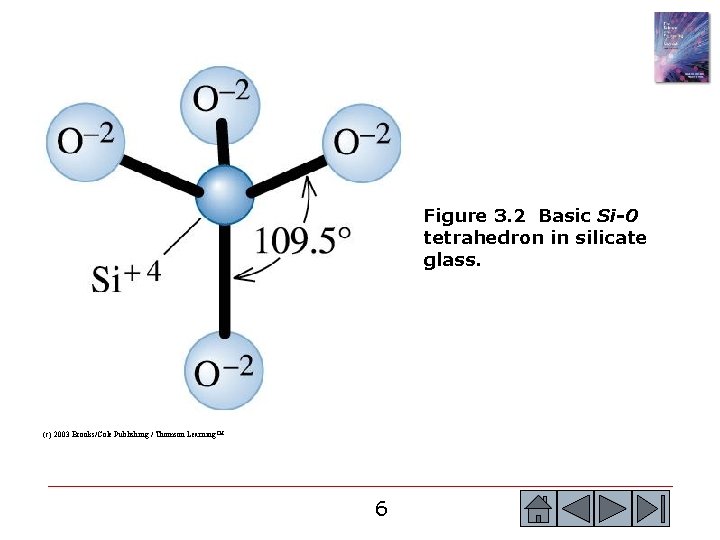
Figure 3. 2 Basic Si-0 tetrahedron in silicate glass. (c) 2003 Brooks/Cole Publishing / Thomson Learning™ 6

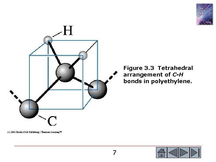
Figure 3. 3 Tetrahedral arrangement of C-H bonds in polyethylene. (c) 2003 Brooks/Cole Publishing / Thomson Learning™ 7

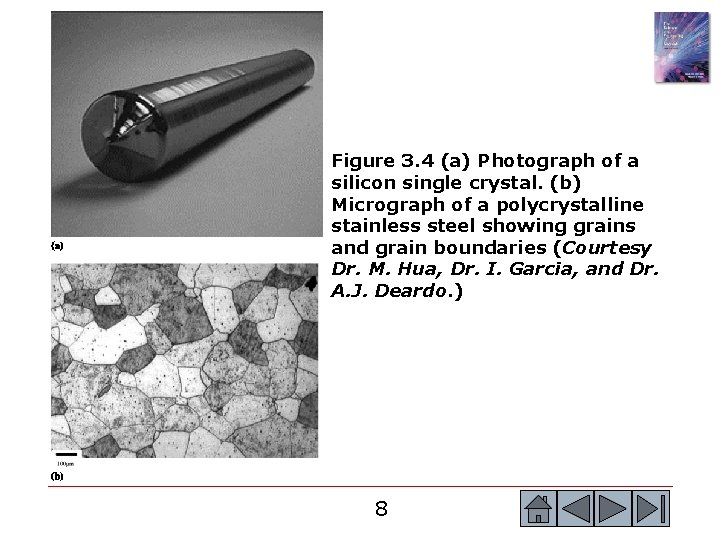
Figure 3. 4 (a) Photograph of a silicon single crystal. (b) Micrograph of a polycrystalline stainless steel showing grains and grain boundaries (Courtesy Dr. M. Hua, Dr. I. Garcia, and Dr. A. J. Deardo. ) 8

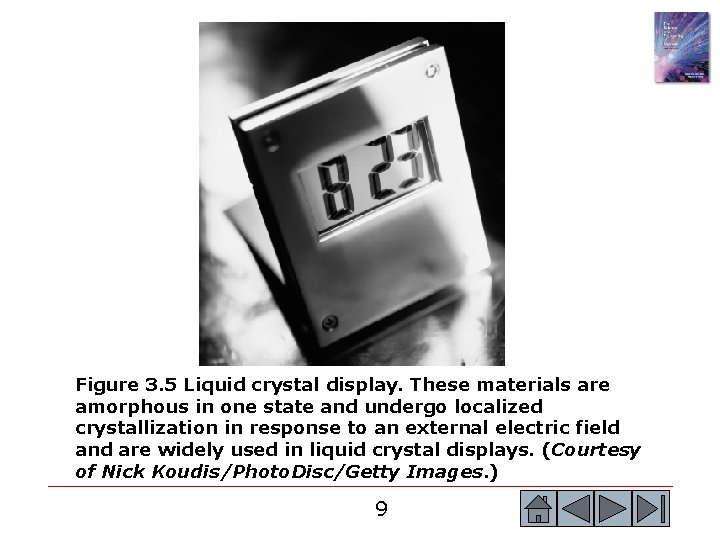
Figure 3. 5 Liquid crystal display. These materials are amorphous in one state and undergo localized crystallization in response to an external electric field and are widely used in liquid crystal displays. (Courtesy of Nick Koudis/Photo. Disc/Getty Images. ) 9

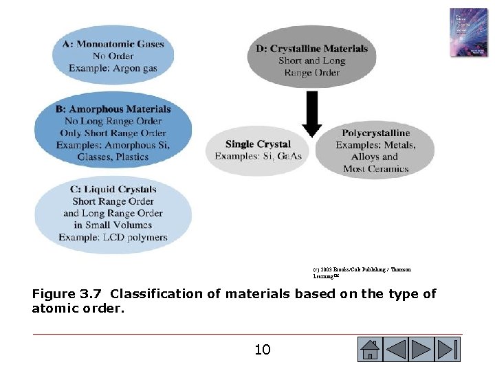
(c) 2003 Brooks/Cole Publishing / Thomson Learning™ Figure 3. 7 Classification of materials based on the type of atomic order. 10

Section 3. 2 Amorphous Materials: Principles and Technological Applications o o o Amorphous materials - Materials, including glasses, that have no long-range order, or crystal structure. Glasses - Solid, non-crystalline materials (typically derived from the molten state) that have only shortrange atomic order. Glass-ceramics - A family of materials typically derived from molten inorganic glasses and processed into crystalline materials with very fine grain size and improved mechanical properties. 11

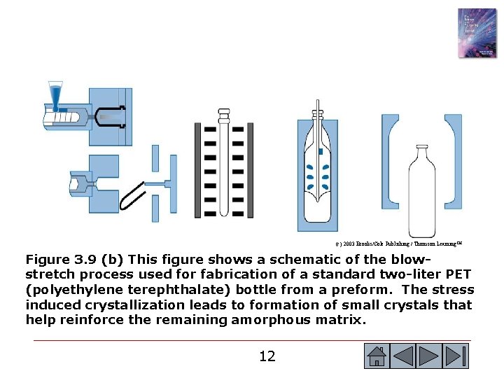
(c) 2003 Brooks/Cole Publishing / Thomson Learning™ Figure 3. 9 (b) This figure shows a schematic of the blowstretch process used for fabrication of a standard two-liter PET (polyethylene terephthalate) bottle from a preform. The stress induced crystallization leads to formation of small crystals that help reinforce the remaining amorphous matrix. 12

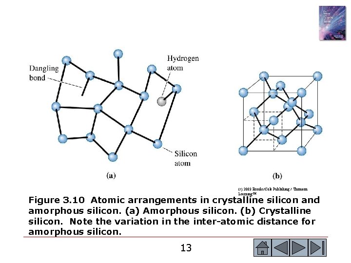
(c) 2003 Brooks/Cole Publishing / Thomson Learning™ Figure 3. 10 Atomic arrangements in crystalline silicon and amorphous silicon. (a) Amorphous silicon. (b) Crystalline silicon. Note the variation in the inter-atomic distance for amorphous silicon. 13

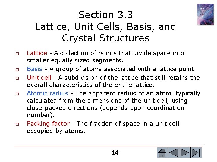
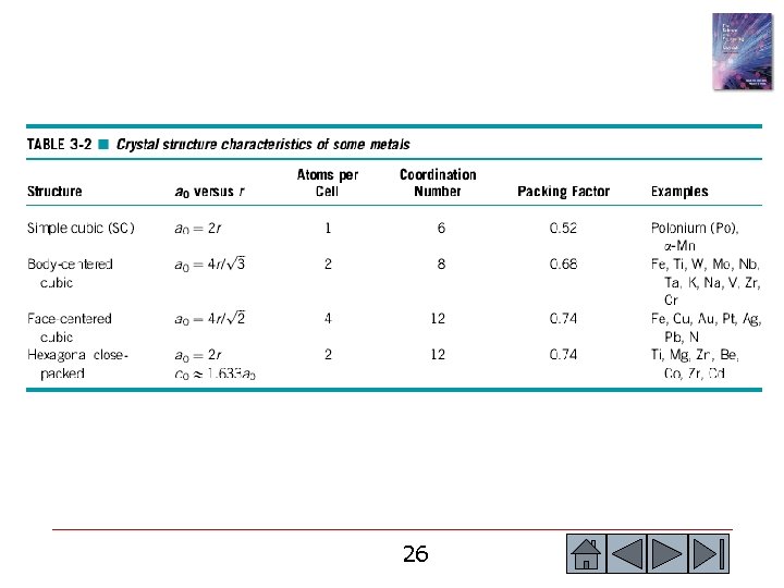
Section 3. 3 Lattice, Unit Cells, Basis, and Crystal Structures o o o Lattice - A collection of points that divide space into smaller equally sized segments. Basis - A group of atoms associated with a lattice point. Unit cell - A subdivision of the lattice that still retains the overall characteristics of the entire lattice. Atomic radius - The apparent radius of an atom, typically calculated from the dimensions of the unit cell, using close-packed directions (depends upon coordination number). Packing factor - The fraction of space in a unit cell occupied by atoms. 14

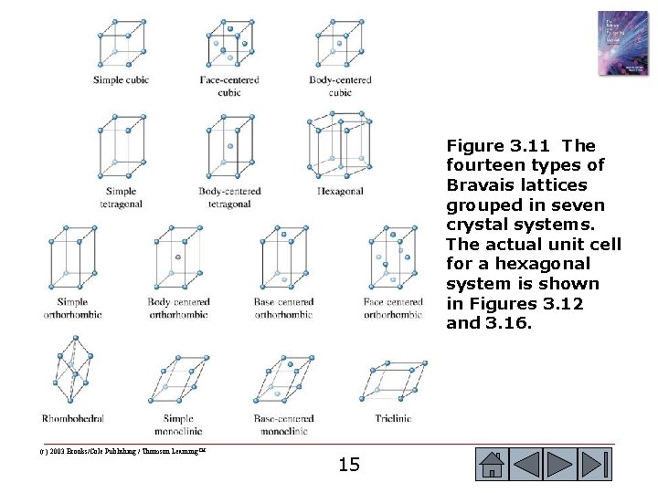
Figure 3. 11 The fourteen types of Bravais lattices grouped in seven crystal systems. The actual unit cell for a hexagonal system is shown in Figures 3. 12 and 3. 16. (c) 2003 Brooks/Cole Publishing / Thomson Learning™ 15

16

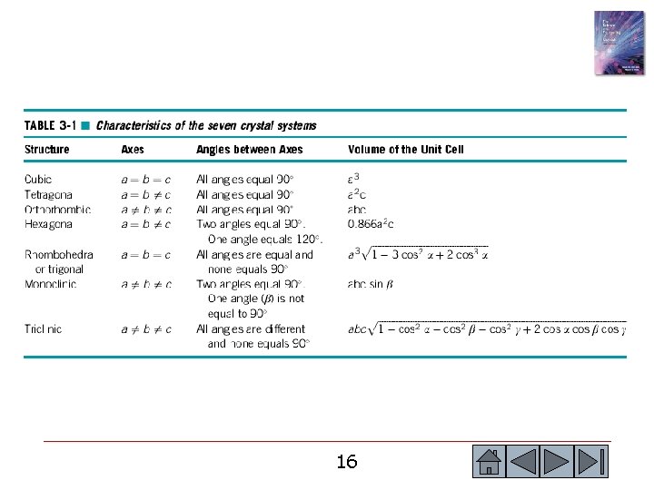
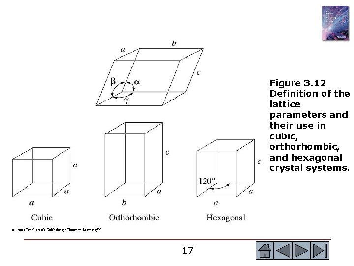
Figure 3. 12 Definition of the lattice parameters and their use in cubic, orthorhombic, and hexagonal crystal systems. (c) 2003 Brooks/Cole Publishing / Thomson Learning™ 17

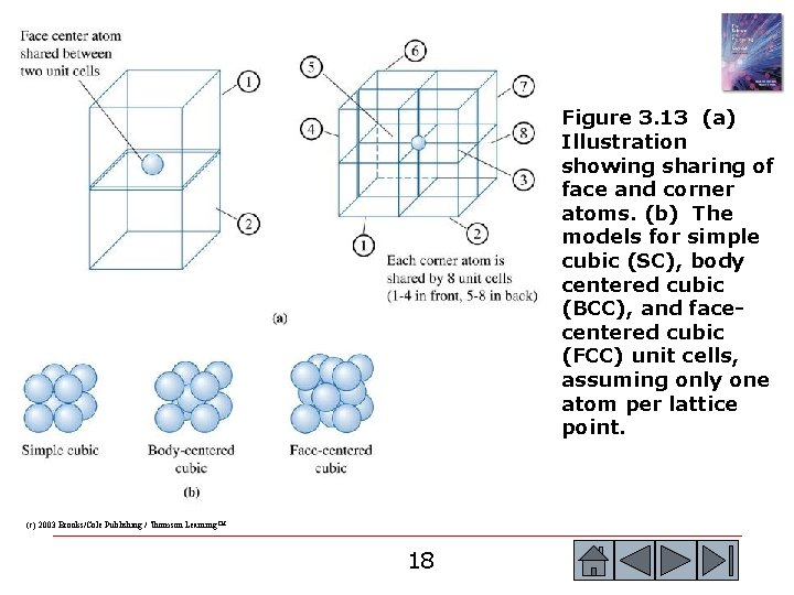
Figure 3. 13 (a) Illustration showing sharing of face and corner atoms. (b) The models for simple cubic (SC), body centered cubic (BCC), and facecentered cubic (FCC) unit cells, assuming only one atom per lattice point. (c) 2003 Brooks/Cole Publishing / Thomson Learning™ 18

Example 3. 1 Determining the Number of Lattice Points in Cubic Crystal Systems Determine the number of lattice points per cell in the cubic crystal systems. If there is only one atom located at each lattice point, calculate the number of atoms per unit cell. Example 3. 1 SOLUTION In the SC unit cell: lattice point / unit cell = (8 corners)1/8 = 1 In BCC unit cells: lattice point / unit cell = (8 corners)1/8 + (1 center)(1) = 2 In FCC unit cells: lattice point / unit cell = (8 corners)1/8 + (6 faces)(1/2) = 4 The number of atoms per unit cell would be 1, 2, and 4, for the simple cubic, body-centered cubic, and face-centered cubic, unit cells, respectively. 19

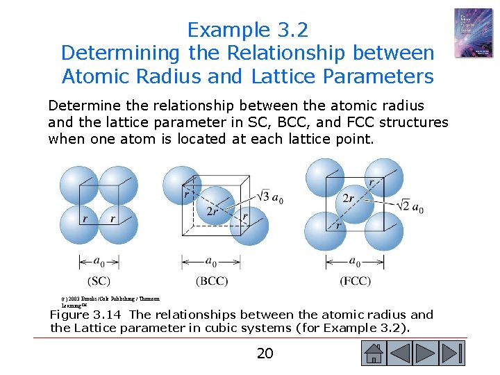
Example 3. 2 Determining the Relationship between Atomic Radius and Lattice Parameters Determine the relationship between the atomic radius and the lattice parameter in SC, BCC, and FCC structures when one atom is located at each lattice point. (c) 2003 Brooks/Cole Publishing / Thomson Learning™ Figure 3. 14 The relationships between the atomic radius and the Lattice parameter in cubic systems (for Example 3. 2). 20

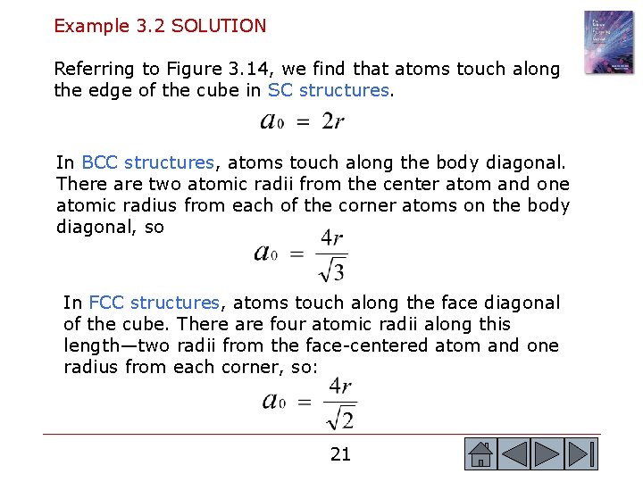
Example 3. 2 SOLUTION Referring to Figure 3. 14, we find that atoms touch along the edge of the cube in SC structures. In BCC structures, atoms touch along the body diagonal. There are two atomic radii from the center atom and one atomic radius from each of the corner atoms on the body diagonal, so In FCC structures, atoms touch along the face diagonal of the cube. There are four atomic radii along this length—two radii from the face-centered atom and one radius from each corner, so: 21

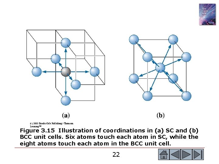
(c) 2003 Brooks/Cole Publishing / Thomson Learning™ Figure 3. 15 Illustration of coordinations in (a) SC and (b) BCC unit cells. Six atoms touch each atom in SC, while the eight atoms touch each atom in the BCC unit cell. 22

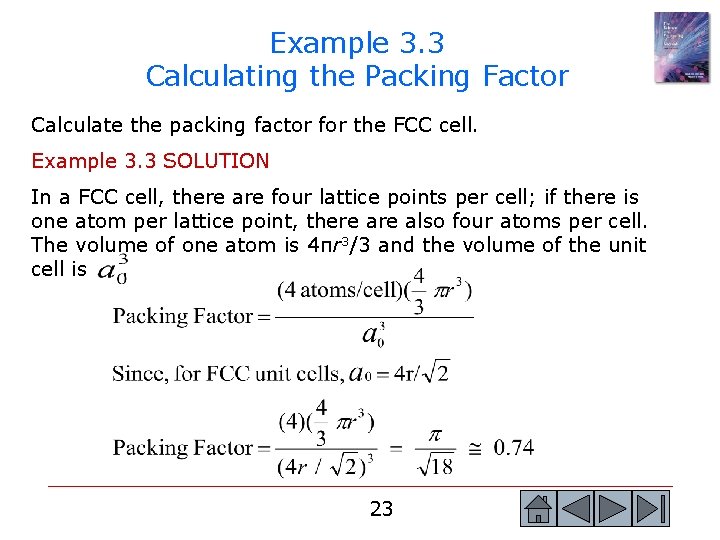
Example 3. 3 Calculating the Packing Factor Calculate the packing factor for the FCC cell. Example 3. 3 SOLUTION In a FCC cell, there are four lattice points per cell; if there is one atom per lattice point, there also four atoms per cell. The volume of one atom is 4πr 3/3 and the volume of the unit cell is. 23

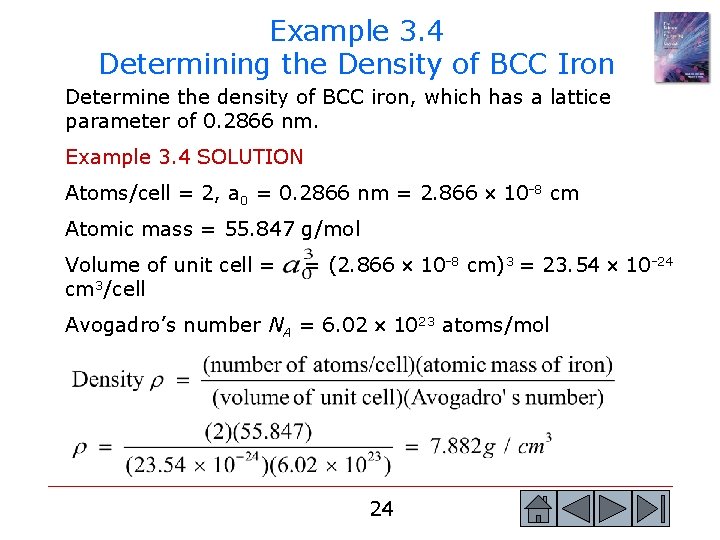
Example 3. 4 Determining the Density of BCC Iron Determine the density of BCC iron, which has a lattice parameter of 0. 2866 nm. Example 3. 4 SOLUTION Atoms/cell = 2, a 0 = 0. 2866 nm = 2. 866 10 -8 cm Atomic mass = 55. 847 g/mol Volume of unit cell = cm 3/cell = (2. 866 10 -8 cm)3 = 23. 54 10 -24 Avogadro’s number NA = 6. 02 1023 atoms/mol 24

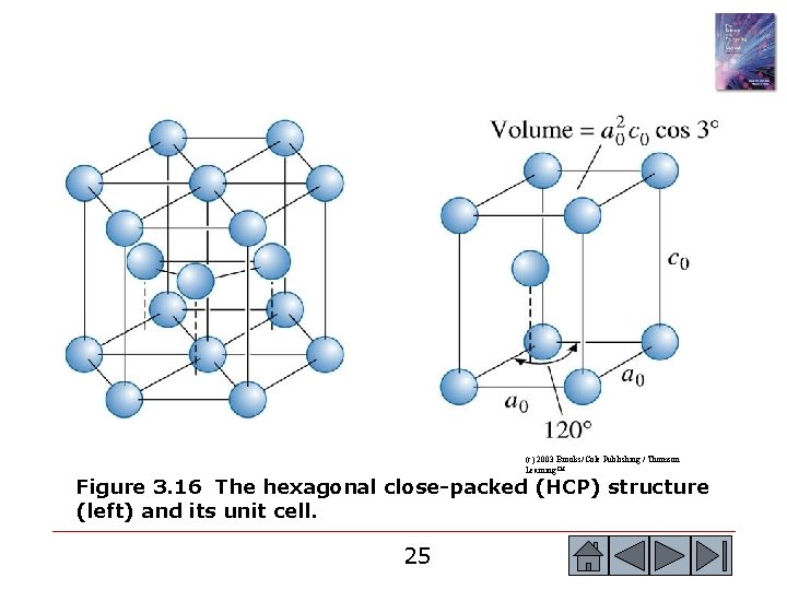
(c) 2003 Brooks/Cole Publishing / Thomson Learning™ Figure 3. 16 The hexagonal close-packed (HCP) structure (left) and its unit cell. 25

26

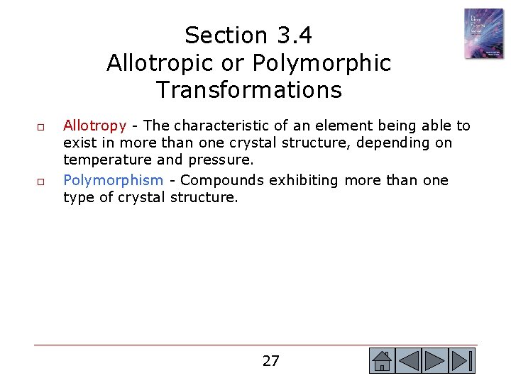
Section 3. 4 Allotropic or Polymorphic Transformations o o Allotropy - The characteristic of an element being able to exist in more than one crystal structure, depending on temperature and pressure. Polymorphism - Compounds exhibiting more than one type of crystal structure. 27

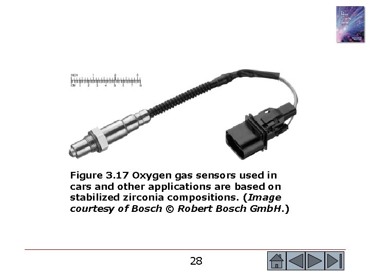
Figure 3. 17 Oxygen gas sensors used in cars and other applications are based on stabilized zirconia compositions. (Image courtesy of Bosch © Robert Bosch Gmb. H. ) 28

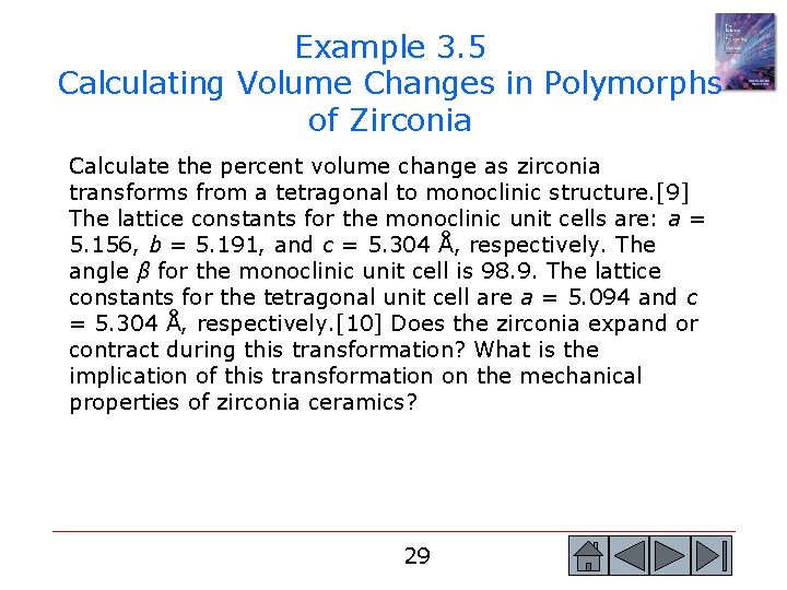
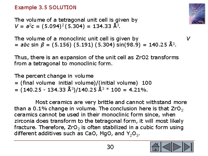
Example 3. 5 Calculating Volume Changes in Polymorphs of Zirconia Calculate the percent volume change as zirconia transforms from a tetragonal to monoclinic structure. [9] The lattice constants for the monoclinic unit cells are: a = 5. 156, b = 5. 191, and c = 5. 304 Å, respectively. The angle β for the monoclinic unit cell is 98. 9. The lattice constants for the tetragonal unit cell are a = 5. 094 and c = 5. 304 Å, respectively. [10] Does the zirconia expand or contract during this transformation? What is the implication of this transformation on the mechanical properties of zirconia ceramics? 29

Example 3. 5 SOLUTION The volume of a tetragonal unit cell is given by V = a 2 c = (5. 094)2 (5. 304) = 134. 33 Å3. The volume of a monoclinic unit cell is given by = abc sin β = (5. 156) (5. 191) (5. 304) sin(98. 9) = 140. 25 Å3. V Thus, there is an expansion of the unit cell as Zr. O 2 transforms from a tetragonal to monoclinic form. The percent change in volume = (final volume initial volume)/(initial volume) 100 = (140. 25 - 134. 33 Å3)/140. 25 Å3 * 100 = 4. 21%. Most ceramics are very brittle and cannot withstand more than a 0. 1% change in volume. The conclusion here is that Zr. O 2 ceramics cannot be used in their monoclinic form since, when zirconia does transform to the tetragonal form, it will most likely fracture. Therefore, Zr. O 2 is often stabilized in a cubic form using different additives such as Ca. O, Mg. O, and Y 2 O 3. 30

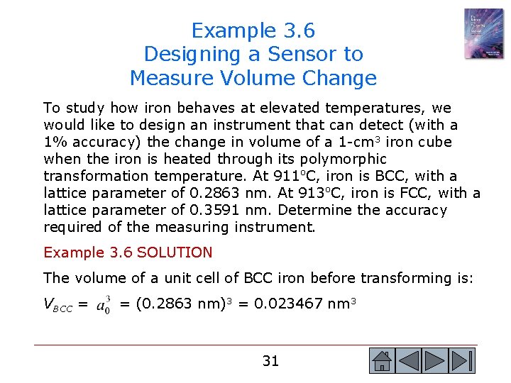
Example 3. 6 Designing a Sensor to Measure Volume Change To study how iron behaves at elevated temperatures, we would like to design an instrument that can detect (with a 1% accuracy) the change in volume of a 1 -cm 3 iron cube when the iron is heated through its polymorphic transformation temperature. At 911 o. C, iron is BCC, with a lattice parameter of 0. 2863 nm. At 913 o. C, iron is FCC, with a lattice parameter of 0. 3591 nm. Determine the accuracy required of the measuring instrument. Example 3. 6 SOLUTION The volume of a unit cell of BCC iron before transforming is: VBCC = = (0. 2863 nm)3 = 0. 023467 nm 3 31

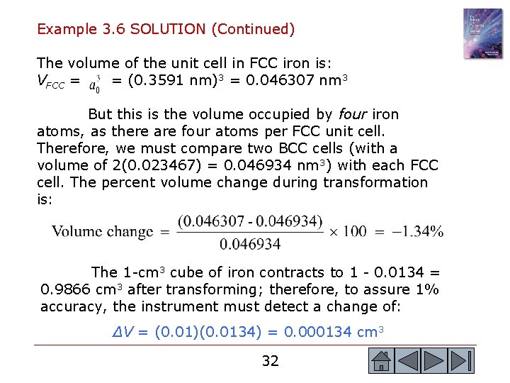
Example 3. 6 SOLUTION (Continued) The volume of the unit cell in FCC iron is: VFCC = = (0. 3591 nm)3 = 0. 046307 nm 3 But this is the volume occupied by four iron atoms, as there are four atoms per FCC unit cell. Therefore, we must compare two BCC cells (with a volume of 2(0. 023467) = 0. 046934 nm 3) with each FCC cell. The percent volume change during transformation is: The 1 -cm 3 cube of iron contracts to 1 - 0. 0134 = 0. 9866 cm 3 after transforming; therefore, to assure 1% accuracy, the instrument must detect a change of: ΔV = (0. 01)(0. 0134) = 0. 000134 cm 3 32

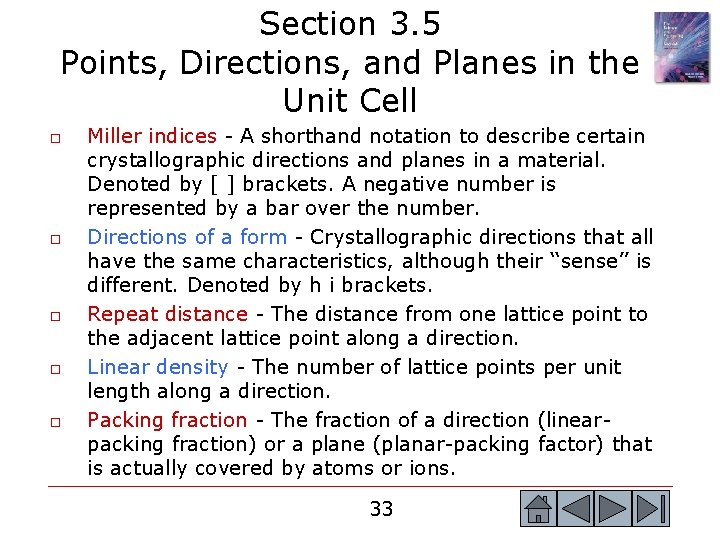
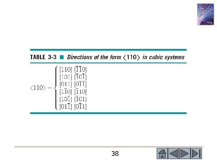
Section 3. 5 Points, Directions, and Planes in the Unit Cell o o o Miller indices - A shorthand notation to describe certain crystallographic directions and planes in a material. Denoted by [ ] brackets. A negative number is represented by a bar over the number. Directions of a form - Crystallographic directions that all have the same characteristics, although their ‘‘sense’’ is different. Denoted by h i brackets. Repeat distance - The distance from one lattice point to the adjacent lattice point along a direction. Linear density - The number of lattice points per unit length along a direction. Packing fraction - The fraction of a direction (linearpacking fraction) or a plane (planar-packing factor) that is actually covered by atoms or ions. 33

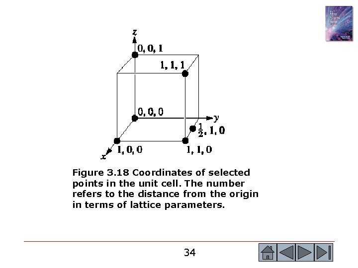
Figure 3. 18 Coordinates of selected points in the unit cell. The number refers to the distance from the origin in terms of lattice parameters. 34

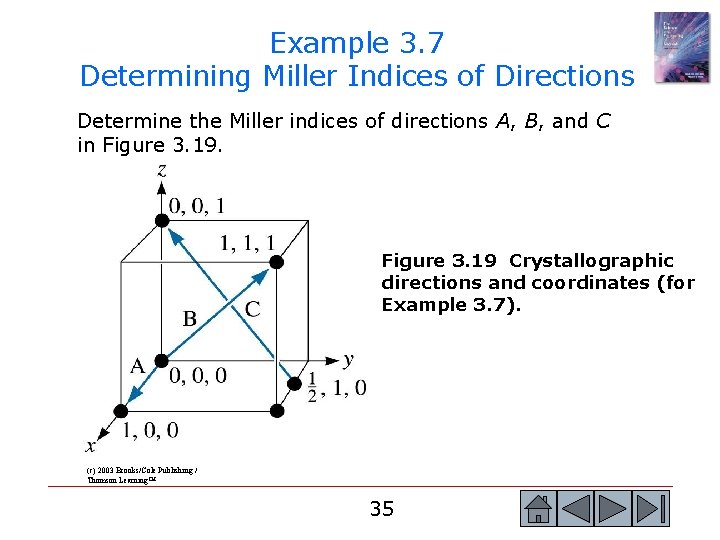
Example 3. 7 Determining Miller Indices of Directions Determine the Miller indices of directions A, B, and C in Figure 3. 19 Crystallographic directions and coordinates (for Example 3. 7). (c) 2003 Brooks/Cole Publishing / Thomson Learning™ 35

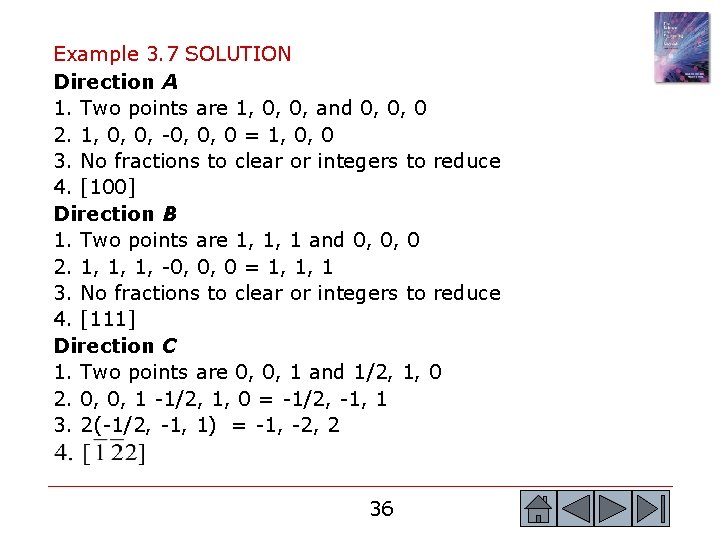
Example 3. 7 SOLUTION Direction A 1. Two points are 1, 0, 0, and 0, 0, 0 2. 1, 0, 0, -0, 0, 0 = 1, 0, 0 3. No fractions to clear or integers to reduce 4. [100] Direction B 1. Two points are 1, 1, 1 and 0, 0, 0 2. 1, 1, 1, -0, 0, 0 = 1, 1, 1 3. No fractions to clear or integers to reduce 4. [111] Direction C 1. Two points are 0, 0, 1 and 1/2, 1, 0 2. 0, 0, 1 -1/2, 1, 0 = -1/2, -1, 1 3. 2(-1/2, -1, 1) = -1, -2, 2 36

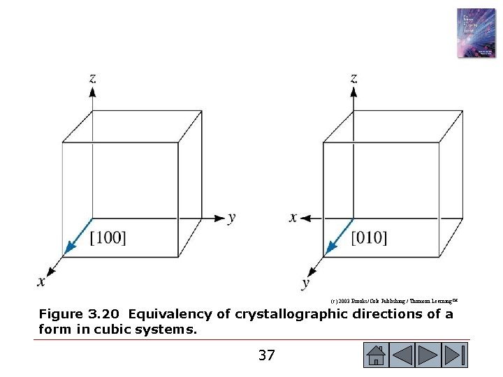
(c) 2003 Brooks/Cole Publishing / Thomson Learning™ Figure 3. 20 Equivalency of crystallographic directions of a form in cubic systems. 37

38
![Figure 3 21 Determining the repeat distance linear density and packing fraction for 110 Figure 3. 21 Determining the repeat distance, linear density, and packing fraction for [110]](https://slidetodoc.com/presentation_image_h/bc9b6aac5c3f32d5f07dda6cbfdafaca/image-39.jpg)
Figure 3. 21 Determining the repeat distance, linear density, and packing fraction for [110] direction in FCC copper. (c) 2003 Brooks/Cole Publishing / Thomson Learning™ 39

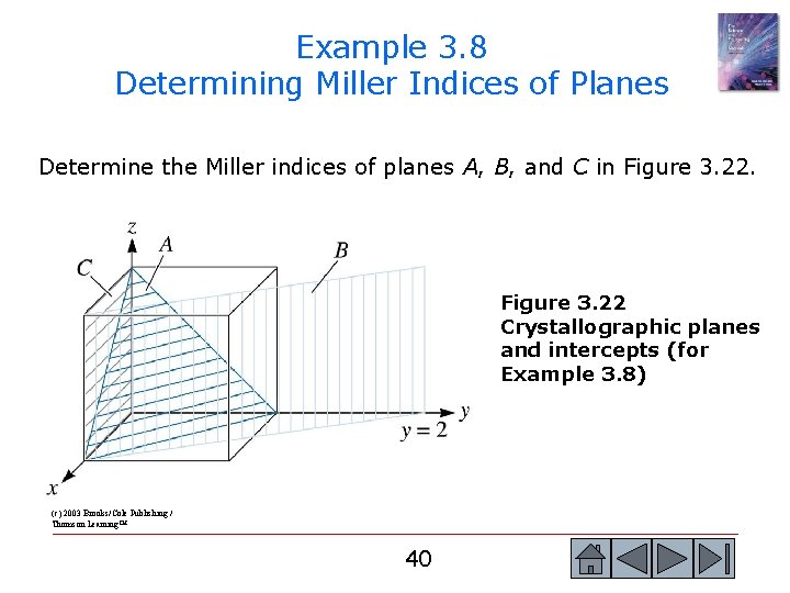
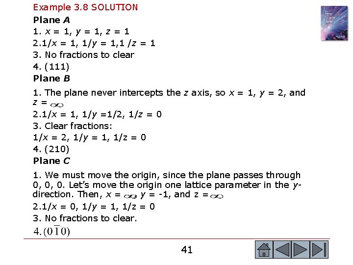
Example 3. 8 Determining Miller Indices of Planes Determine the Miller indices of planes A, B, and C in Figure 3. 22 Crystallographic planes and intercepts (for Example 3. 8) (c) 2003 Brooks/Cole Publishing / Thomson Learning™ 40

Example 3. 8 SOLUTION Plane A 1. x = 1, y = 1, z = 1 2. 1/x = 1, 1/y = 1, 1 /z = 1 3. No fractions to clear 4. (111) Plane B 1. The plane never intercepts the z axis, so x = 1, y = 2, and z= 2. 1/x = 1, 1/y =1/2, 1/z = 0 3. Clear fractions: 1/x = 2, 1/y = 1, 1/z = 0 4. (210) Plane C 1. We must move the origin, since the plane passes through 0, 0, 0. Let’s move the origin one lattice parameter in the ydirection. Then, x = , y = -1, and z = 2. 1/x = 0, 1/y = 1, 1/z = 0 3. No fractions to clear. 41

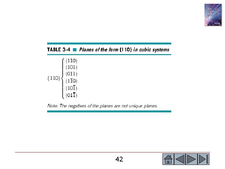
42

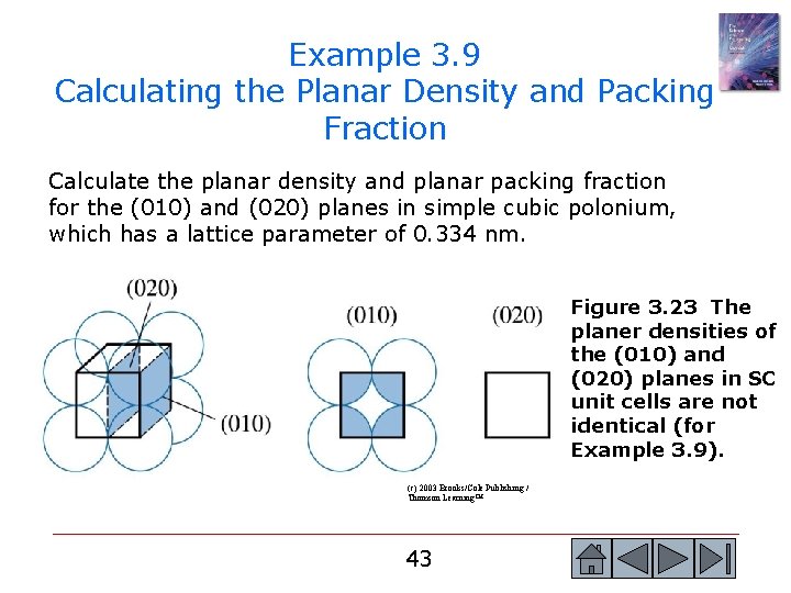
Example 3. 9 Calculating the Planar Density and Packing Fraction Calculate the planar density and planar packing fraction for the (010) and (020) planes in simple cubic polonium, which has a lattice parameter of 0. 334 nm. Figure 3. 23 The planer densities of the (010) and (020) planes in SC unit cells are not identical (for Example 3. 9). (c) 2003 Brooks/Cole Publishing / Thomson Learning™ 43

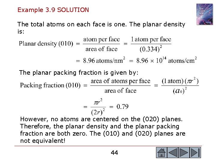
Example 3. 9 SOLUTION The total atoms on each face is one. The planar density is: The planar packing fraction is given by: However, no atoms are centered on the (020) planes. Therefore, the planar density and the planar packing fraction are both zero. The (010) and (020) planes are not equivalent! 44

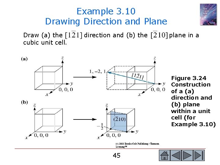
Example 3. 10 Drawing Direction and Plane Draw (a) the cubic unit cell. direction and (b) the plane in a Figure 3. 24 Construction of a (a) direction and (b) plane within a unit cell (for Example 3. 10) (c) 2003 Brooks/Cole Publishing / Thomson Learning™ 45

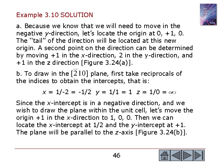
Example 3. 10 SOLUTION a. Because we know that we will need to move in the negative y-direction, let’s locate the origin at 0, +1, 0. The ‘‘tail’’ of the direction will be located at this new origin. A second point on the direction can be determined by moving +1 in the x-direction, 2 in the y-direction, and +1 in the z direction [Figure 3. 24(a)]. b. To draw in the plane, first take reciprocals of the indices to obtain the intercepts, that is: x = 1/-2 = -1/2 y = 1/1 = 1 z = 1/0 = Since the x-intercept is in a negative direction, and we wish to draw the plane within the unit cell, let’s move the origin +1 in the x-direction to 1, 0, 0. Then we can locate the x-intercept at 1/2 and the y-intercept at +1. The plane will be parallel to the z-axis [Figure 3. 24(b)]. 46

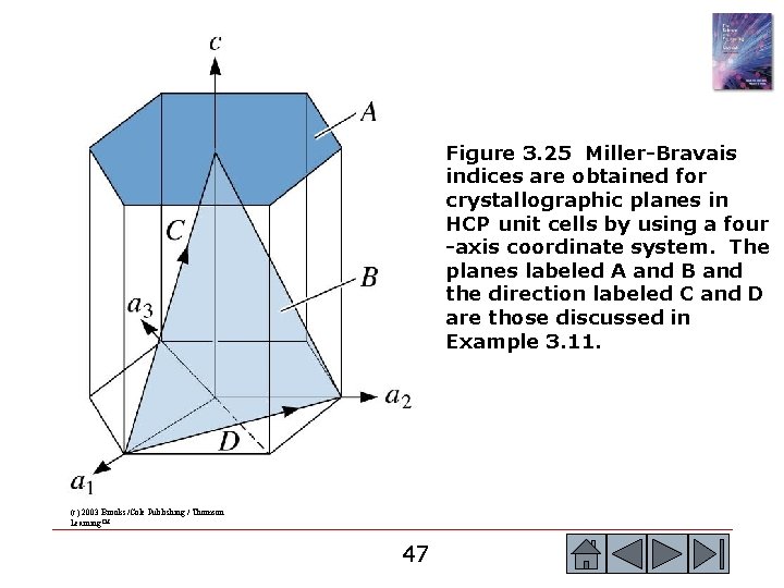
Figure 3. 25 Miller-Bravais indices are obtained for crystallographic planes in HCP unit cells by using a four -axis coordinate system. The planes labeled A and B and the direction labeled C and D are those discussed in Example 3. 11. (c) 2003 Brooks/Cole Publishing / Thomson Learning™ 47

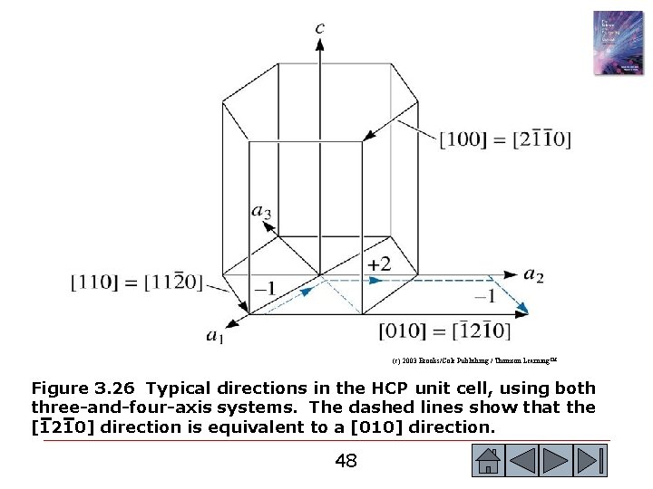
(c) 2003 Brooks/Cole Publishing / Thomson Learning™ Figure 3. 26 Typical directions in the HCP unit cell, using both three-and-four-axis systems. The dashed lines show that the [1210] direction is equivalent to a [010] direction. 48

Example 3. 11 Determining the Miller-Bravais Indices for Planes and Directions Determine the Miller-Bravais indices for planes A and B and directions C and D in Figure 3. 25 Miller-Bravais indices are obtained for crystallographic planes in HCP unit cells by using a four-axis coordinate system. The planes labeled A and B and the direction labeled C and D are those discussed in Example 3. 11. (c) 2003 Brooks/Cole Publishing / Thomson Learning™ 49

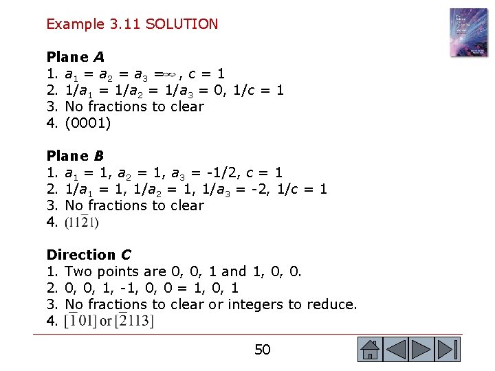
Example 3. 11 SOLUTION Plane A 1. a 1 = a 2 = a 3 = , c = 1 2. 1/a 1 = 1/a 2 = 1/a 3 = 0, 1/c = 1 3. No fractions to clear 4. (0001) Plane B 1. a 1 = 1, a 2 = 1, a 3 = -1/2, c = 1 2. 1/a 1 = 1, 1/a 2 = 1, 1/a 3 = -2, 1/c = 1 3. No fractions to clear 4. Direction C 1. Two points are 0, 0, 1 and 1, 0, 0. 2. 0, 0, 1, -1, 0, 0 = 1, 0, 1 3. No fractions to clear or integers to reduce. 4. 50

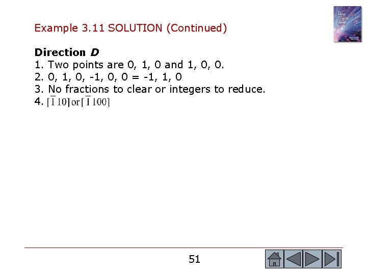
Example 3. 11 SOLUTION (Continued) Direction D 1. Two points are 0, 1, 0 and 1, 0, 0. 2. 0, 1, 0, -1, 0, 0 = -1, 1, 0 3. No fractions to clear or integers to reduce. 4. 51

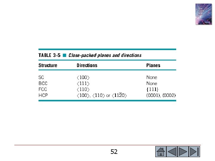
52

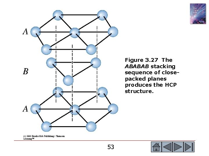
Figure 3. 27 The ABABAB stacking sequence of closepacked planes produces the HCP structure. (c) 2003 Brooks/Cole Publishing / Thomson Learning™ 53

(c) 2003 Brooks/Cole Publishing / Thomson Learning™ Figure 3. 28 The ABCABCABC stacking sequence of close-packed planes produces the FCC structure. 54

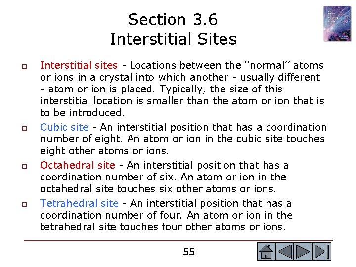
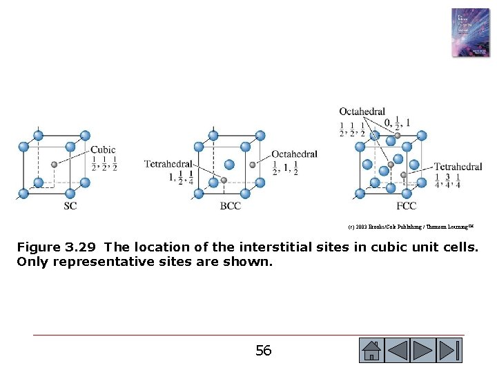
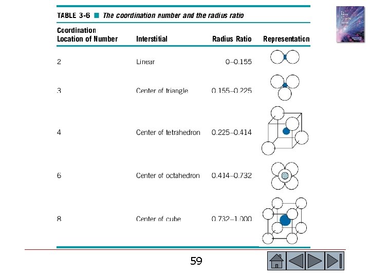
Section 3. 6 Interstitial Sites o o Interstitial sites - Locations between the ‘‘normal’’ atoms or ions in a crystal into which another - usually different - atom or ion is placed. Typically, the size of this interstitial location is smaller than the atom or ion that is to be introduced. Cubic site - An interstitial position that has a coordination number of eight. An atom or ion in the cubic site touches eight other atoms or ions. Octahedral site - An interstitial position that has a coordination number of six. An atom or ion in the octahedral site touches six other atoms or ions. Tetrahedral site - An interstitial position that has a coordination number of four. An atom or ion in the tetrahedral site touches four other atoms or ions. 55

(c) 2003 Brooks/Cole Publishing / Thomson Learning™ Figure 3. 29 The location of the interstitial sites in cubic unit cells. Only representative sites are shown. 56

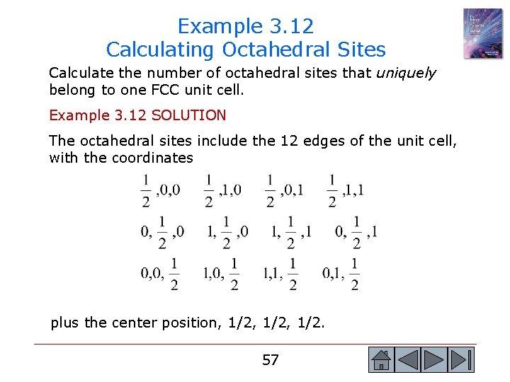
Example 3. 12 Calculating Octahedral Sites Calculate the number of octahedral sites that uniquely belong to one FCC unit cell. Example 3. 12 SOLUTION The octahedral sites include the 12 edges of the unit cell, with the coordinates plus the center position, 1/2, 1/2. 57

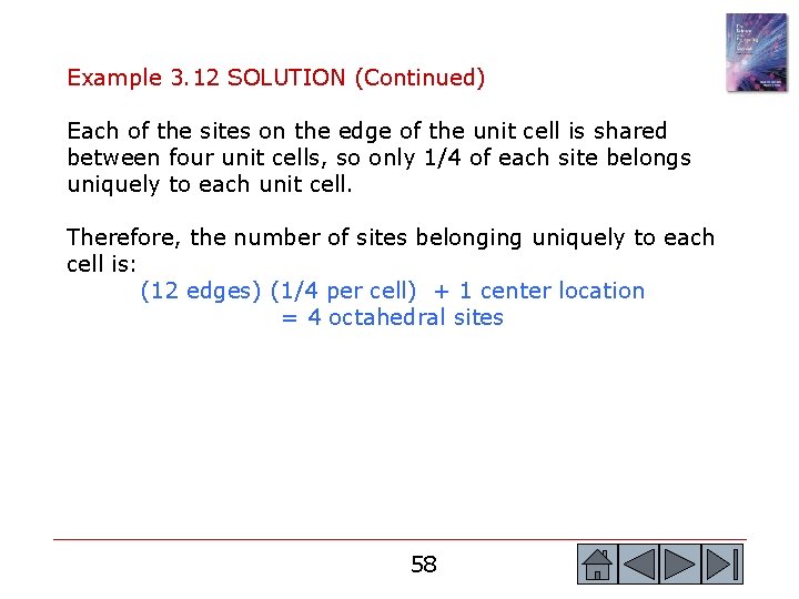
Example 3. 12 SOLUTION (Continued) Each of the sites on the edge of the unit cell is shared between four unit cells, so only 1/4 of each site belongs uniquely to each unit cell. Therefore, the number of sites belonging uniquely to each cell is: (12 edges) (1/4 per cell) + 1 center location = 4 octahedral sites 58

59

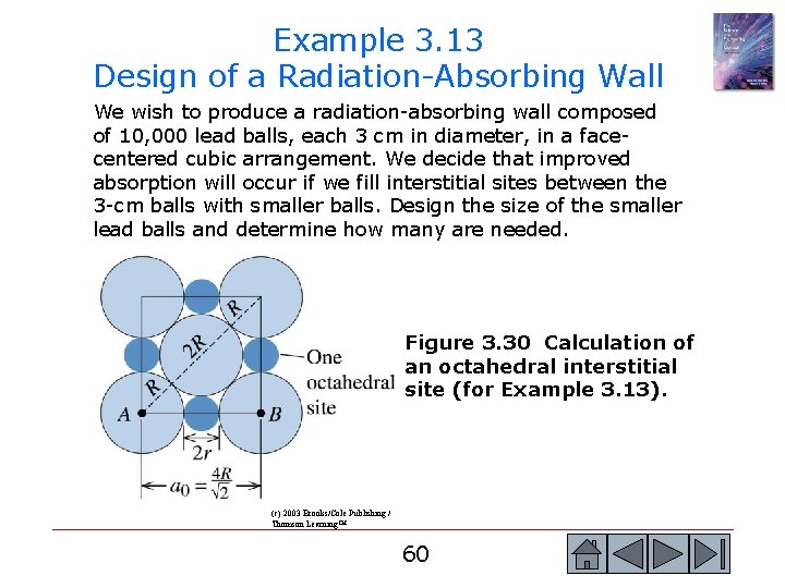
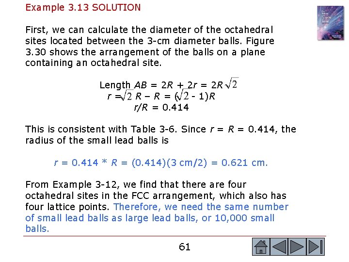
Example 3. 13 Design of a Radiation-Absorbing Wall We wish to produce a radiation-absorbing wall composed of 10, 000 lead balls, each 3 cm in diameter, in a facecentered cubic arrangement. We decide that improved absorption will occur if we fill interstitial sites between the 3 -cm balls with smaller balls. Design the size of the smaller lead balls and determine how many are needed. Figure 3. 30 Calculation of an octahedral interstitial site (for Example 3. 13). (c) 2003 Brooks/Cole Publishing / Thomson Learning™ 60

Example 3. 13 SOLUTION First, we can calculate the diameter of the octahedral sites located between the 3 -cm diameter balls. Figure 3. 30 shows the arrangement of the balls on a plane containing an octahedral site. Length AB = 2 R + 2 r = 2 R r = R – R = ( - 1)R r/R = 0. 414 This is consistent with Table 3 -6. Since r = R = 0. 414, the radius of the small lead balls is r = 0. 414 * R = (0. 414)(3 cm/2) = 0. 621 cm. From Example 3 -12, we find that there are four octahedral sites in the FCC arrangement, which also has four lattice points. Therefore, we need the same number of small lead balls as large lead balls, or 10, 000 small balls. 61

Section 3. 7 Crystal Structures of Ionic Materials o Factors need to be considered in order to understand crystal structures of ionically bonded solids: § Ionic Radii § Electrical Neutrality § Connection between Anion Polyhedra § Visualization of Crystal Structures Using Computers 62

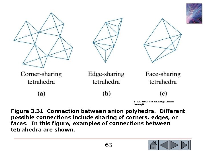
(c) 2003 Brooks/Cole Publishing / Thomson Learning™ Figure 3. 31 Connection between anion polyhedra. Different possible connections include sharing of corners, edges, or faces. In this figure, examples of connections between tetrahedra are shown. 63

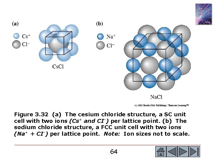
(c) 2003 Brooks/Cole Publishing / Thomson Learning™ Figure 3. 32 (a) The cesium chloride structure, a SC unit cell with two ions (Cs+ and CI-) per lattice point. (b) The sodium chloride structure, a FCC unit cell with two ions (Na+ + CI-) per lattice point. Note: Ion sizes not to scale. 64

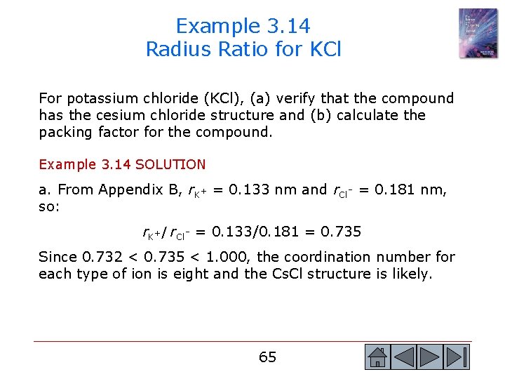
Example 3. 14 Radius Ratio for KCl For potassium chloride (KCl), (a) verify that the compound has the cesium chloride structure and (b) calculate the packing factor for the compound. Example 3. 14 SOLUTION a. From Appendix B, r. K+ = 0. 133 nm and r. Cl- = 0. 181 nm, so: r. K+/ r. Cl- = 0. 133/0. 181 = 0. 735 Since 0. 732 < 0. 735 < 1. 000, the coordination number for each type of ion is eight and the Cs. Cl structure is likely. 65

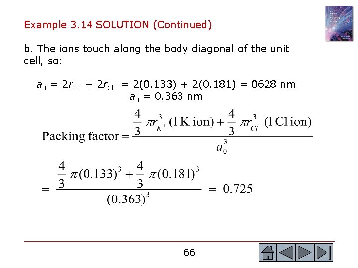
Example 3. 14 SOLUTION (Continued) b. The ions touch along the body diagonal of the unit cell, so: a 0 = 2 r. K+ + 2 r. Cl- = 2(0. 133) + 2(0. 181) = 0628 nm a 0 = 0. 363 nm 66

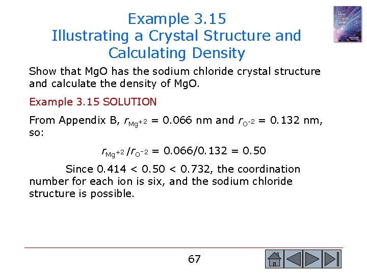
Example 3. 15 Illustrating a Crystal Structure and Calculating Density Show that Mg. O has the sodium chloride crystal structure and calculate the density of Mg. O. Example 3. 15 SOLUTION From Appendix B, r. Mg+2 = 0. 066 nm and r. O-2 = 0. 132 nm, so: r. Mg+2 /r. O-2 = 0. 066/0. 132 = 0. 50 Since 0. 414 < 0. 50 < 0. 732, the coordination number for each ion is six, and the sodium chloride structure is possible. 67

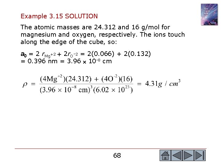
Example 3. 15 SOLUTION The atomic masses are 24. 312 and 16 g/mol for magnesium and oxygen, respectively. The ions touch along the edge of the cube, so: a 0 = 2 r. Mg+2 + 2 r. O-2 = 2(0. 066) + 2(0. 132) = 0. 396 nm = 3. 96 10 -8 cm 68

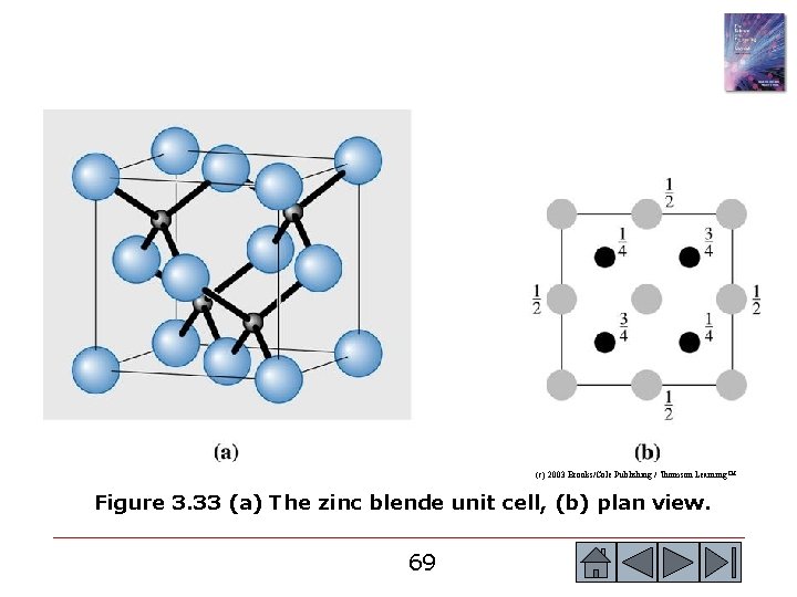
(c) 2003 Brooks/Cole Publishing / Thomson Learning™ Figure 3. 33 (a) The zinc blende unit cell, (b) plan view. 69

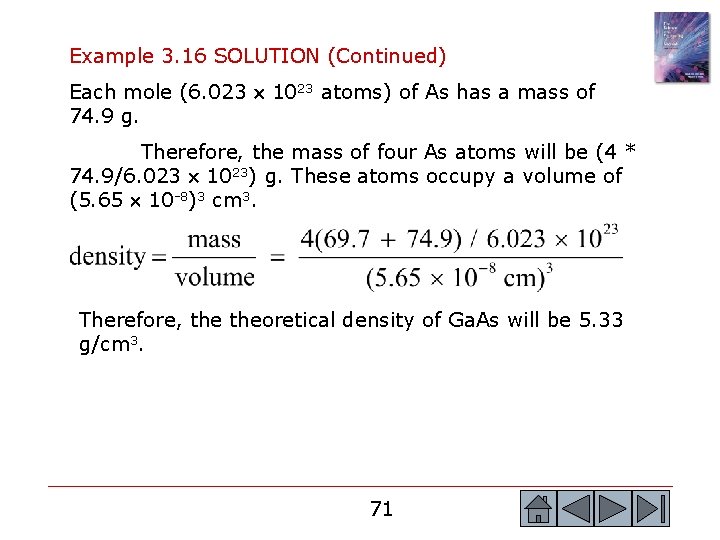
Example 3. 16 Calculating the Theoretical Density of Ga. As The lattice constant of gallium arsenide (Ga. As) is 5. 65 Å. Show that theoretical density of Ga. As is 5. 33 g/cm 3. Example 3. 16 SOLUTION For the ‘‘zinc blende’’ Ga. As unit cell, there are four Ga and four As atoms per unit cell. From the periodic table (Chapter 2): Each mole (6. 023 1023 atoms) of Ga has a mass of 69. 7 g. Therefore, the mass of four Ga atoms will be (4 * 69. 7/6. 023 1023) g. 70

Example 3. 16 SOLUTION (Continued) Each mole (6. 023 1023 atoms) of As has a mass of 74. 9 g. Therefore, the mass of four As atoms will be (4 * 74. 9/6. 023 1023) g. These atoms occupy a volume of (5. 65 10 -8)3 cm 3. Therefore, theoretical density of Ga. As will be 5. 33 g/cm 3. 71

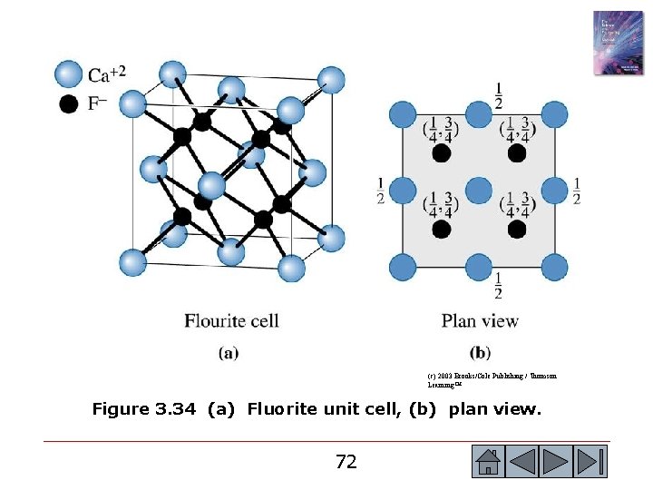
(c) 2003 Brooks/Cole Publishing / Thomson Learning™ Figure 3. 34 (a) Fluorite unit cell, (b) plan view. 72

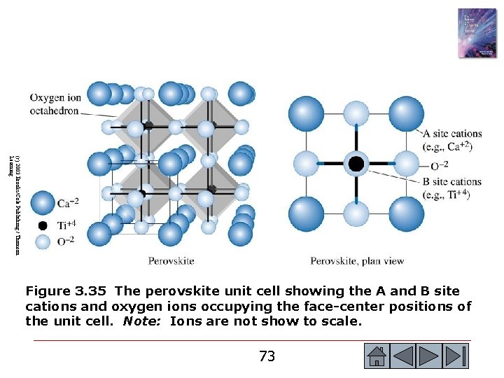
(c) 2003 Brooks/Cole Publishing / Thomson Learning Figure 3. 35 The perovskite unit cell showing the A and B site cations and oxygen ions occupying the face-center positions of the unit cell. Note: Ions are not show to scale. 73

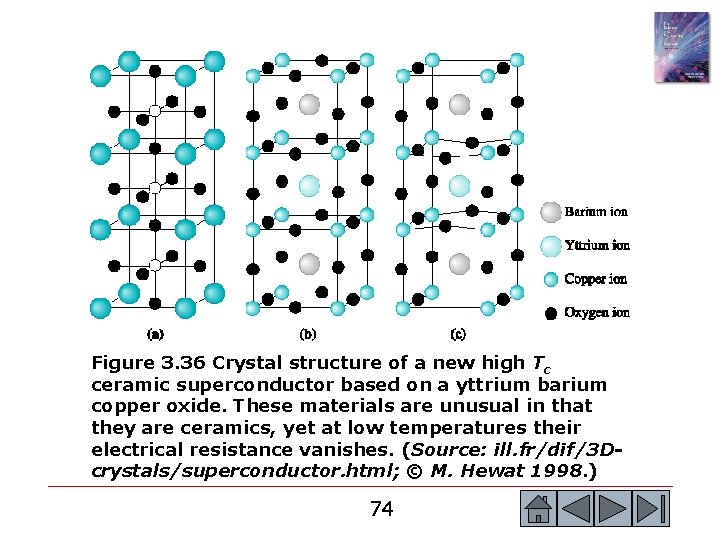
Figure 3. 36 Crystal structure of a new high Tc ceramic superconductor based on a yttrium barium copper oxide. These materials are unusual in that they are ceramics, yet at low temperatures their electrical resistance vanishes. (Source: ill. fr/dif/3 Dcrystals/superconductor. html; © M. Hewat 1998. ) 74

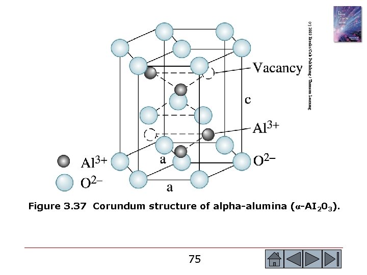
(c) 2003 Brooks/Cole Publishing / Thomson Learning Figure 3. 37 Corundum structure of alpha-alumina (α-AI 203). 75

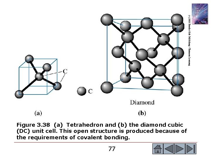
Section 3. 8 Covalent Structures o o Covalently bonded materials frequently have complex structures in order to satisfy the directional restraints imposed by the bonding. Diamond cubic (DC) - A special type of face-centered cubic crystal structure found in carbon, silicon, and other covalently bonded materials. 76

(c) 2003 Brooks/Cole Publishing / Thomson Learning Figure 3. 38 (a) Tetrahedron and (b) the diamond cubic (DC) unit cell. This open structure is produced because of the requirements of covalent bonding. 77

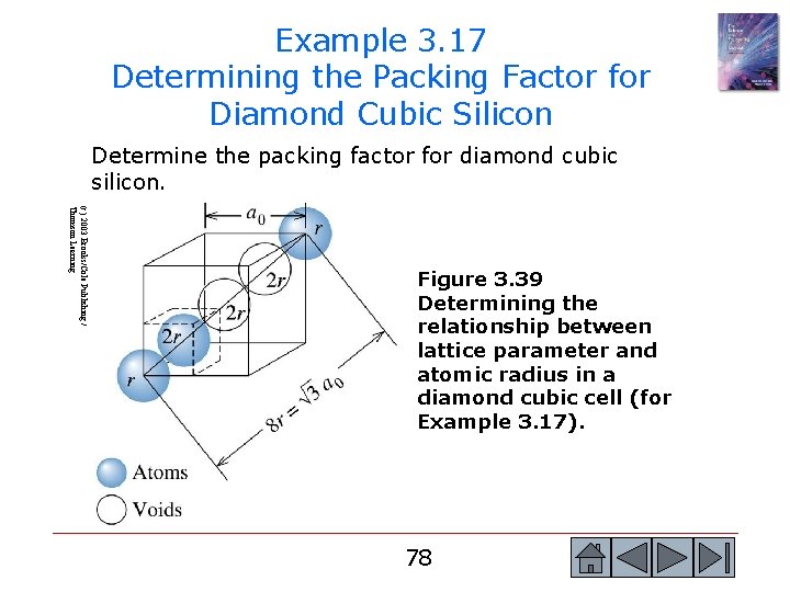
Example 3. 17 Determining the Packing Factor for Diamond Cubic Silicon Determine the packing factor for diamond cubic silicon. (c) 2003 Brooks/Cole Publishing / Thomson Learning Figure 3. 39 Determining the relationship between lattice parameter and atomic radius in a diamond cubic cell (for Example 3. 17). 78

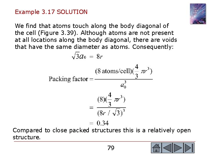
Example 3. 17 SOLUTION We find that atoms touch along the body diagonal of the cell (Figure 3. 39). Although atoms are not present at all locations along the body diagonal, there are voids that have the same diameter as atoms. Consequently: Compared to close packed structures this is a relatively open structure. 79

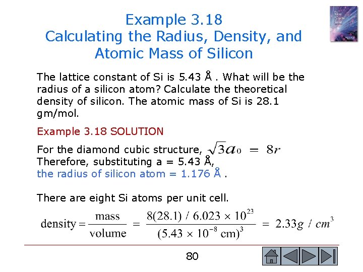
Example 3. 18 Calculating the Radius, Density, and Atomic Mass of Silicon The lattice constant of Si is 5. 43 Å. What will be the radius of a silicon atom? Calculate theoretical density of silicon. The atomic mass of Si is 28. 1 gm/mol. Example 3. 18 SOLUTION For the diamond cubic structure, Therefore, substituting a = 5. 43 Å, the radius of silicon atom = 1. 176 Å. There are eight Si atoms per unit cell. 80

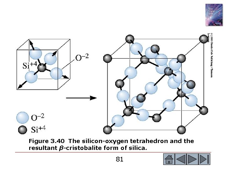
(c) 2003 Brooks/Cole Publishing / Thomson Learning Figure 3. 40 The silicon-oxygen tetrahedron and the resultant β-cristobalite form of silica. 81

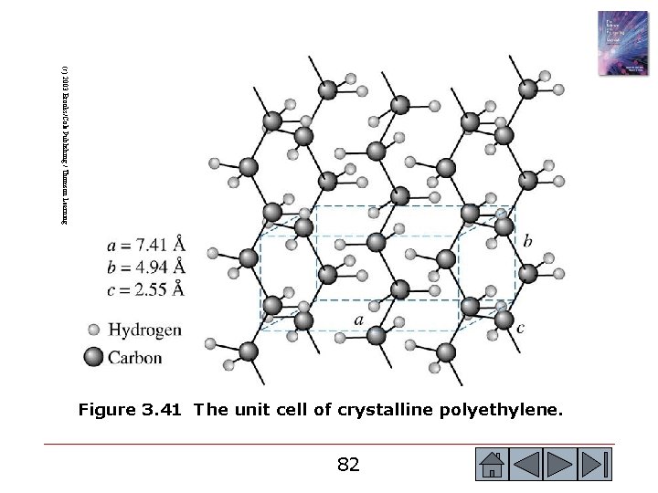
(c) 2003 Brooks/Cole Publishing / Thomson Learning Figure 3. 41 The unit cell of crystalline polyethylene. 82

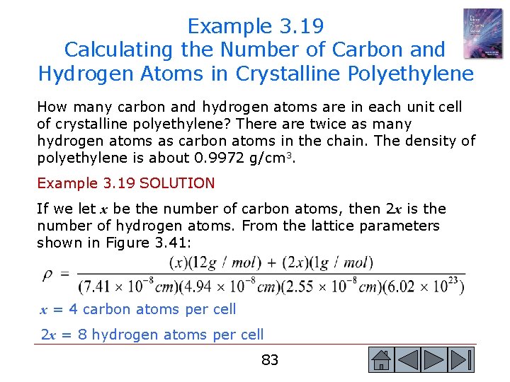
Example 3. 19 Calculating the Number of Carbon and Hydrogen Atoms in Crystalline Polyethylene How many carbon and hydrogen atoms are in each unit cell of crystalline polyethylene? There are twice as many hydrogen atoms as carbon atoms in the chain. The density of polyethylene is about 0. 9972 g/cm 3. Example 3. 19 SOLUTION If we let x be the number of carbon atoms, then 2 x is the number of hydrogen atoms. From the lattice parameters shown in Figure 3. 41: x = 4 carbon atoms per cell 2 x = 8 hydrogen atoms per cell 83

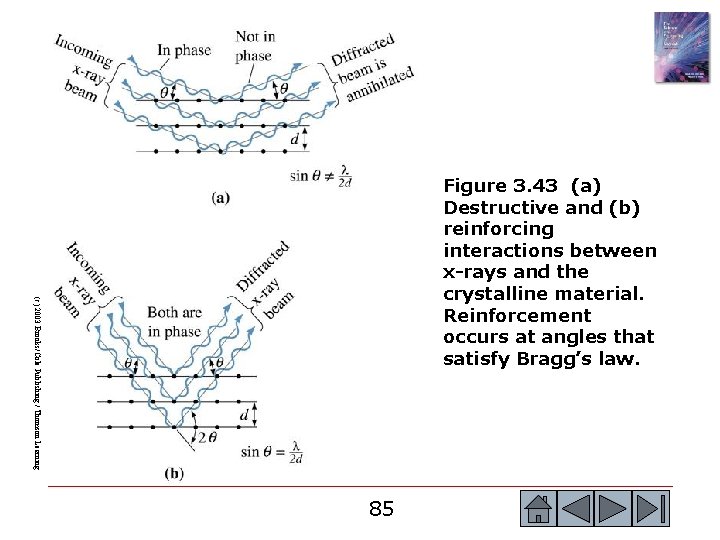
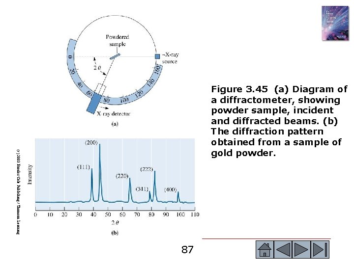
Section 3. 9 Diffraction Techniques for Crystal Structure Analysis o o o Diffraction - The constructive interference, or reinforcement, of a beam of x-rays or electrons interacting with a material. The diffracted beam provides useful information concerning the structure of the material. Bragg’s law - The relationship describing the angle at which a beam of x-rays of a particular wavelength diffracts from crystallographic planes of a given interplanar spacing. In a diffractometer a moving x-ray detector records the 2 y angles at which the beam is diffracted, giving a characteristic diffraction pattern 84

(c) 2003 Brooks/Cole Publishing / Thomson Learning Figure 3. 43 (a) Destructive and (b) reinforcing interactions between x-rays and the crystalline material. Reinforcement occurs at angles that satisfy Bragg’s law. 85

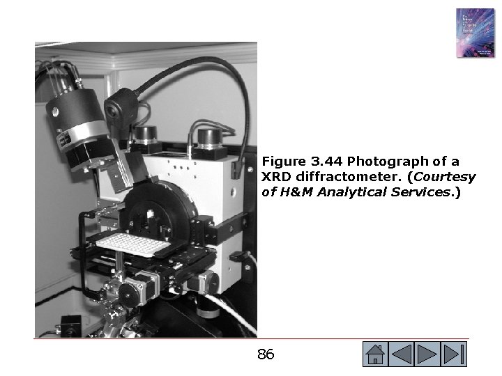
Figure 3. 44 Photograph of a XRD diffractometer. (Courtesy of H&M Analytical Services. ) 86

(c) 2003 Brooks/Cole Publishing / Thomson Learning Figure 3. 45 (a) Diagram of a diffractometer, showing powder sample, incident and diffracted beams. (b) The diffraction pattern obtained from a sample of gold powder. 87

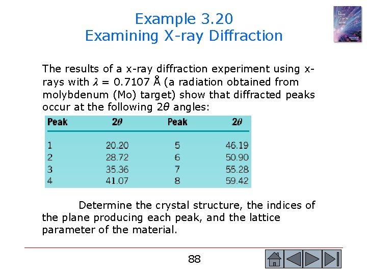
Example 3. 20 Examining X-ray Diffraction The results of a x-ray diffraction experiment using xrays with λ = 0. 7107 Å (a radiation obtained from molybdenum (Mo) target) show that diffracted peaks occur at the following 2θ angles: Determine the crystal structure, the indices of the plane producing each peak, and the lattice parameter of the material. 88

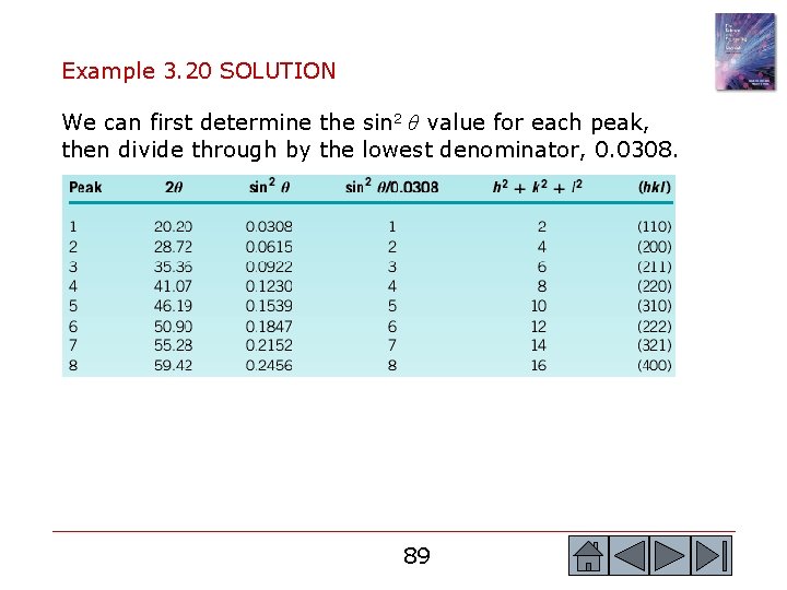
Example 3. 20 SOLUTION We can first determine the sin 2 θ value for each peak, then divide through by the lowest denominator, 0. 0308. 89

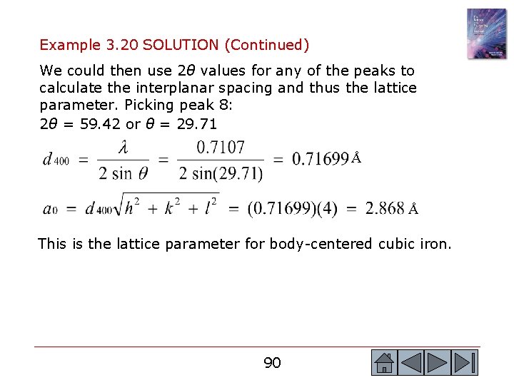
Example 3. 20 SOLUTION (Continued) We could then use 2θ values for any of the peaks to calculate the interplanar spacing and thus the lattice parameter. Picking peak 8: 2θ = 59. 42 or θ = 29. 71 Å Å This is the lattice parameter for body-centered cubic iron. 90

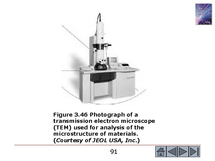
Figure 3. 46 Photograph of a transmission electron microscope (TEM) used for analysis of the microstructure of materials. (Courtesy of JEOL USA, Inc. ) 91

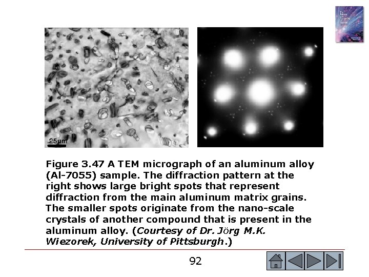
Figure 3. 47 A TEM micrograph of an aluminum alloy (Al-7055) sample. The diffraction pattern at the right shows large bright spots that represent diffraction from the main aluminum matrix grains. The smaller spots originate from the nano-scale crystals of another compound that is present in the aluminum alloy. (Courtesy of Dr. JÖrg M. K. Wiezorek, University of Pittsburgh. ) 92

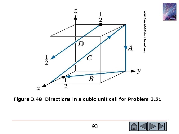
(c) 2003 Brooks/Cole Publishing / Thomson Learning Figure 3. 48 Directions in a cubic unit cell for Problem 3. 51 93

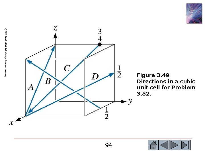
(c) 2003 Brooks/Cole Publishing / Thomson Learning Figure 3. 49 Directions in a cubic unit cell for Problem 3. 52. 94

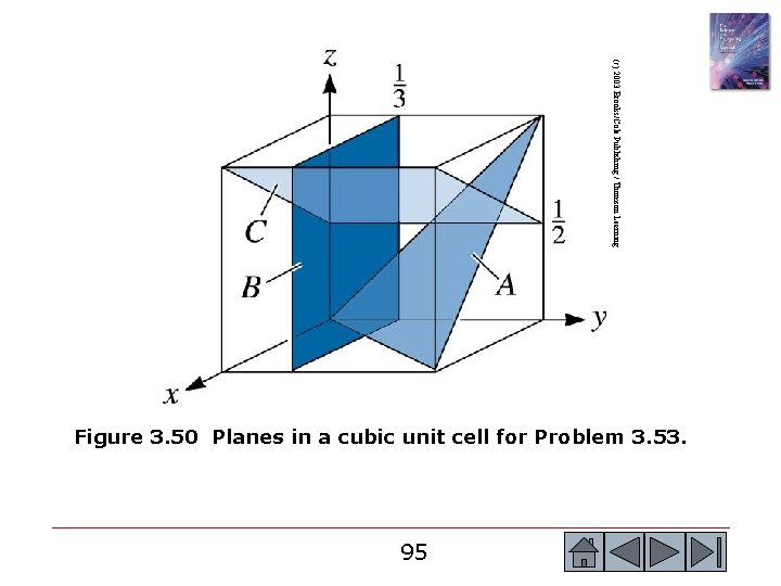
(c) 2003 Brooks/Cole Publishing / Thomson Learning Figure 3. 50 Planes in a cubic unit cell for Problem 3. 53. 95

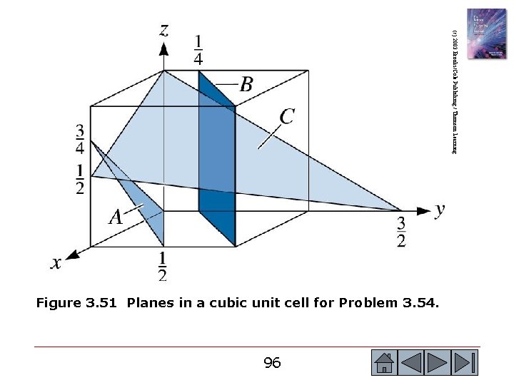
(c) 2003 Brooks/Cole Publishing / Thomson Learning Figure 3. 51 Planes in a cubic unit cell for Problem 3. 54. 96

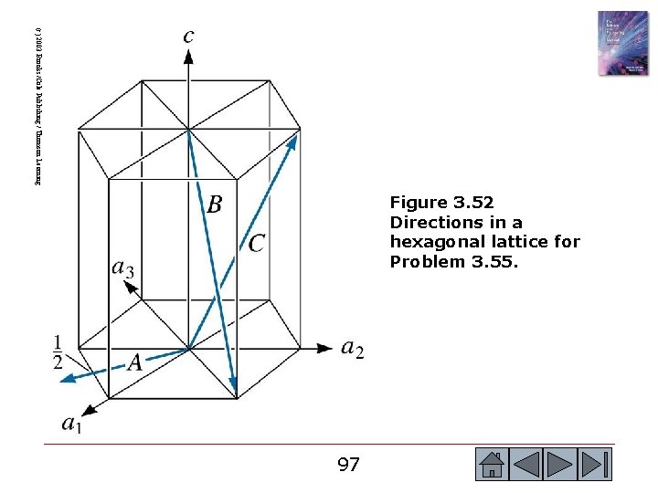
(c) 2003 Brooks/Cole Publishing / Thomson Learning Figure 3. 52 Directions in a hexagonal lattice for Problem 3. 55. 97

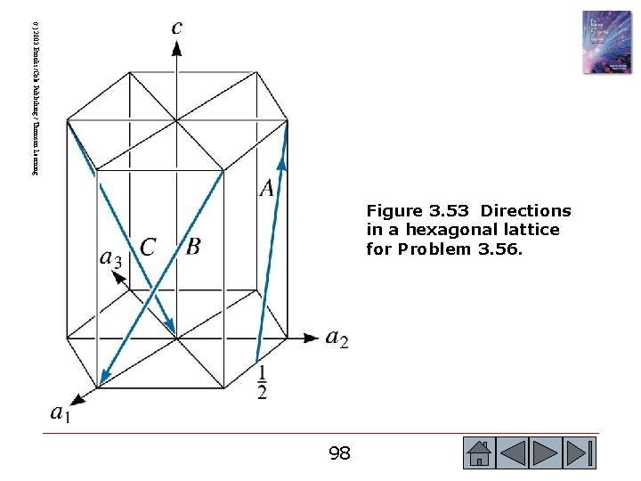
(c) 2003 Brooks/Cole Publishing / Thomson Learning Figure 3. 53 Directions in a hexagonal lattice for Problem 3. 56. 98

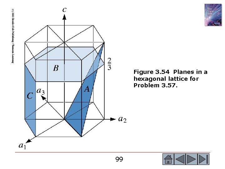
(c) 2003 Brooks/Cole Publishing / Thomson Learning Figure 3. 54 Planes in a hexagonal lattice for Problem 3. 57. 99

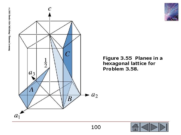
(c) 2003 Brooks/Cole Publishing / Thomson Learning Figure 3. 55 Planes in a hexagonal lattice for Problem 3. 58. 100

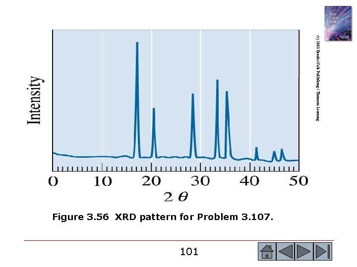
(c) 2003 Brooks/Cole Publishing / Thomson Learning Figure 3. 56 XRD pattern for Problem 3. 107. 101

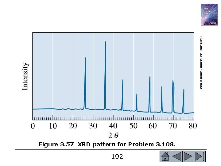
(c) 2003 Brooks/Cole Publishing / Thomson Learning Figure 3. 57 XRD pattern for Problem 3. 108. 102