The REX Neo A New Processor Architecture for


- Slides: 28

The REX Neo: A New Processor Architecture for Exascale and Beyond Thomas Sohmers March 24 th 2016 SOS 20

Team: Founders Thomas Sohmers, Founder and CEO. Worked at the MIT Institute for Soldier Nanotechnologies for 3 years as both an end user of HPC systems, and later transitioned into designing and building them at the lab. This experience led to starting REX Computing in 2013 as a recipient of Peter Thiel’s “ 20 Under 20” Fellowship, where he leads architectural design and operations. Thomas has been featured on Forbes’ 30 under 30 list and is a project lead for the Open Compute Project HPC Group. Paul Sebexen, CTO. Paul started programming as a child, and studied CS at Georgia Tech. He has worked in fields including structural biology, theoretical ecology, and nanofabrication. Paul was part of the 2012 class of Thiel Fellows, where he founded a synthetic biology startup and worked at Lawrence Berkeley National lab for 18 months. He later joined Thomas in starting REX, where he contributes an extensive knowledge of low level software and tool development. © 2016 REX Computing 2

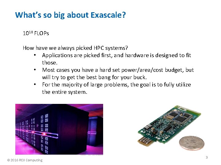
What’s so big about Exascale? 1018 FLOPs How have we always picked HPC systems? • Applications are picked first, and hardware is designed to fit those. • Most cases you have a hard set power/area/cost budget, but will try to get the best bang for your buck. • For the majority of large problems, the goal is to fully utilize the entire system. © 2016 REX Computing 3

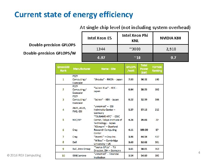
Current state of energy efficiency At single chip level (not including system overhead) Double-precision GFLOPS/W © 2016 REX Computing Intel Xeon E 5 Intel Xeon Phi KNL NVIDIA K 80 1344 ~3000 2, 910 4. 97 ~10 9. 7 4

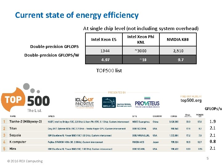
Current state of energy efficiency At single chip level (not including system overhead) Double-precision GFLOPS/W Intel Xeon E 5 Intel Xeon Phi KNL NVIDIA K 80 1344 ~3000 2, 910 4. 97 ~10 9. 7 TOP 500 list GFLOPs/w 1. 9 2. 1 0. 8 2. 1 © 2016 REX Computing 5

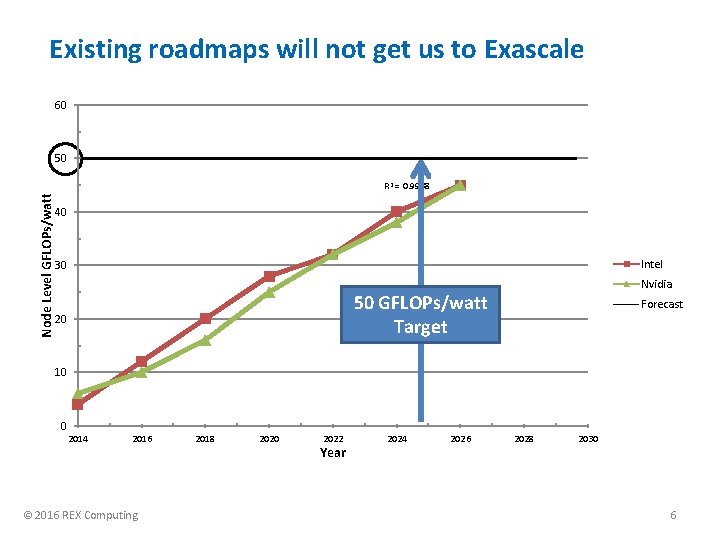
Existing roadmaps will not get us to Exascale 60 50 Node Level GFLOPs/watt R 2 = 0. 9938 40 Intel 30 Nvidia 50 GFLOPs/watt Target 20 Forecast 10 0 2014 2016 © 2016 REX Computing 2018 2020 2022 Year 2024 2026 2028 2030 6

REX Computing is a new approach to efficient computing, redefining how processors are designed and where computing occurs. REX Computing Neo © 2016 REX Computing 7

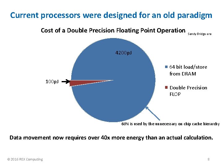
Current processors were designed for an old paradigm Cost of a Double Precision Floating Point Operation Sandy Bridge era 4200 p. J 64 bit load/store from DRAM 100 p. J Double Precision FLOP 60% is used by the unnecessary on chip cache hierarchy Data movement now requires over 40 x more energy than an actual calculation. © 2016 REX Computing 8

A short history of caches “You can’t fake memory bandwidth that isn’t there” –Seymour Cray • Caches are great… • Hide latency due to slow main memory • CDC 6600 (1964) with instruction stack through the initial Motorola 68 k (1982) instruction caches. It only started to get bad when chip designers had a bunch of “free” transistors. • Except kills power efficiency when implementing virtual memory • IBM System 360 Model 67 (1967) was the first to implement Virtual Memory with what we would now call a MMU (at that point a “Dynamic Translation Box”) • Additional logic for TLBs and other logic on a modern chip uses 30%50% of the die area. • Virtual Memory translation and paging are two of the worst decisions in computing history • Makes things a bit easier for a programmer when you assume you have bad compilers, but at significant hardware (power, area, and latency) cost. © 2016 REX Computing 9

A short history of caches cont. • Chip designers got lazy with VLSI • Intel 286 (1982) was one of the first commercial chips to implement memory protection, and expanded upon the memory segmentation of the 8086. • Intel 386 (1986) was the first to implement an external cache (16 to 64 K), but it was not replicating anything higher up in the hierarchy. • The 486 (1989) was the first to implement an 8 K on die cache. • The Pentium and Pentium Pro continued this trend, implementing a managed cache hierarchy followed by a second level of cache. • Introduction of hardware managed caching is what I consider “The beginning of the end”, in which additional hardware complexity was acceptable due to not caring how many transistors were used, as they were get faster, lower power, and cheaper every year. • This does not work well once the power wall (End of Dennard Scaling) was reached, and is starting to completely break down with the end of Moore’s law approaching. © 2016 REX Computing 10

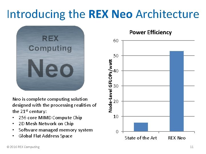
Introducing the REX Neo Architecture Power Efficiency REX Computing Neo is complete computing solution designed with the processing realities of the 21 st century: • 256 core MIMD Compute Chip • 2 D Mesh Network on Chip • Software managed memory system • Global Flat Address Space © 2016 REX Computing 50 Node-Level GFLOPs/watt Neo 60 40 30 20 10 0 State of the Art REX Neo 11

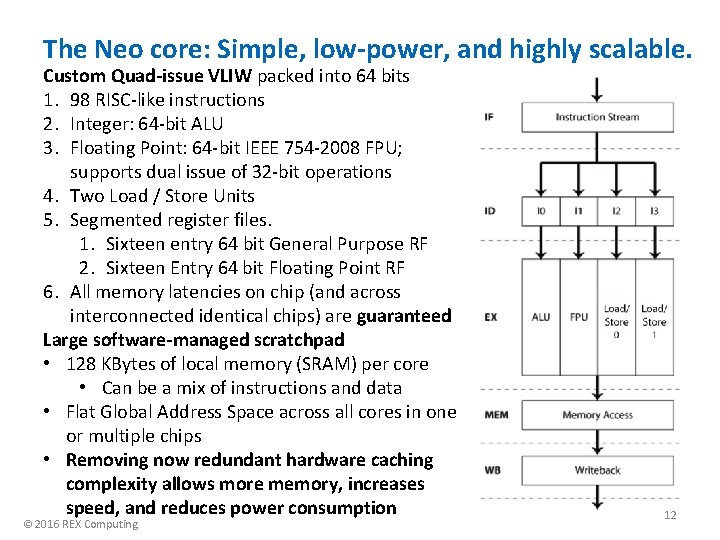
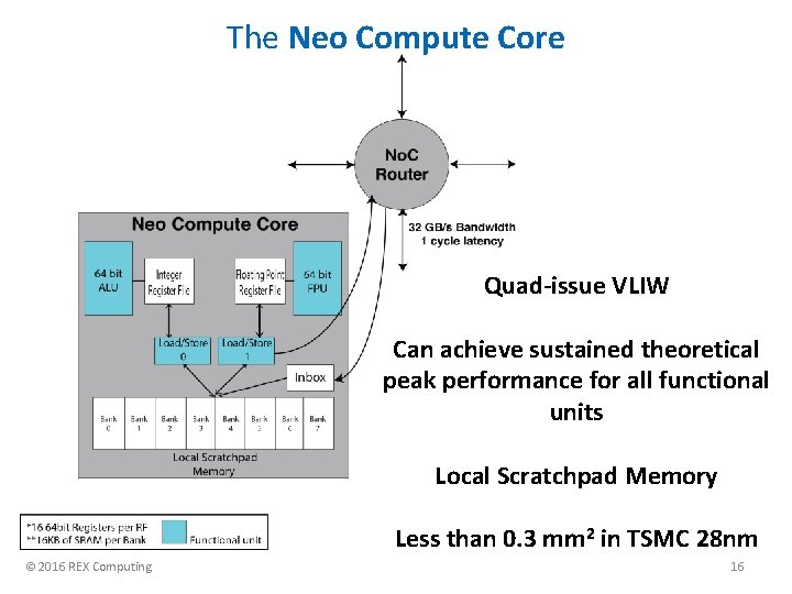
The Neo core: Simple, low-power, and highly scalable. Custom Quad-issue VLIW packed into 64 bits 1. 98 RISC-like instructions 2. Integer: 64 -bit ALU 3. Floating Point: 64 -bit IEEE 754 -2008 FPU; supports dual issue of 32 -bit operations 4. Two Load / Store Units 5. Segmented register files. 1. Sixteen entry 64 bit General Purpose RF 2. Sixteen Entry 64 bit Floating Point RF 6. All memory latencies on chip (and across interconnected identical chips) are guaranteed Large software-managed scratchpad • 128 KBytes of local memory (SRAM) per core • Can be a mix of instructions and data • Flat Global Address Space across all cores in one or multiple chips • Removing now redundant hardware caching complexity allows more memory, increases speed, and reduces power consumption © 2016 REX Computing 12

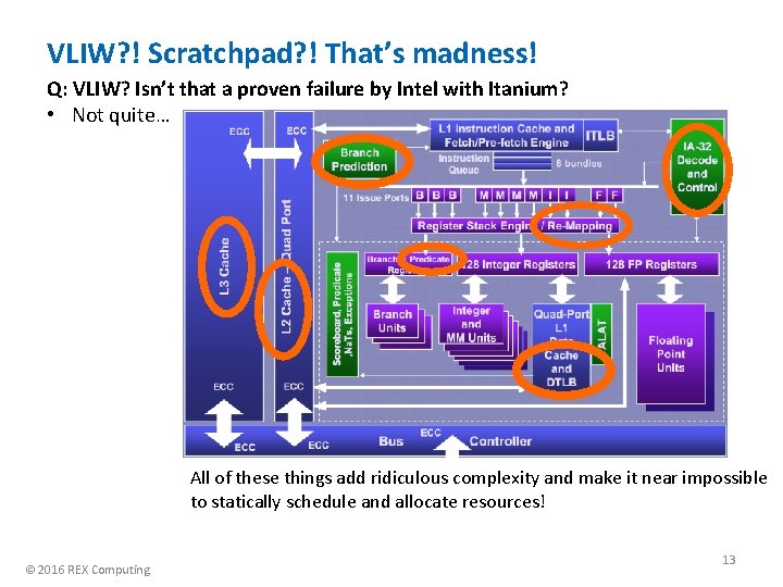
VLIW? ! Scratchpad? ! That’s madness! Q: VLIW? Isn’t that a proven failure by Intel with Itanium? • Not quite… All of these things add ridiculous complexity and make it near impossible to statically schedule and allocate resources! © 2016 REX Computing 13

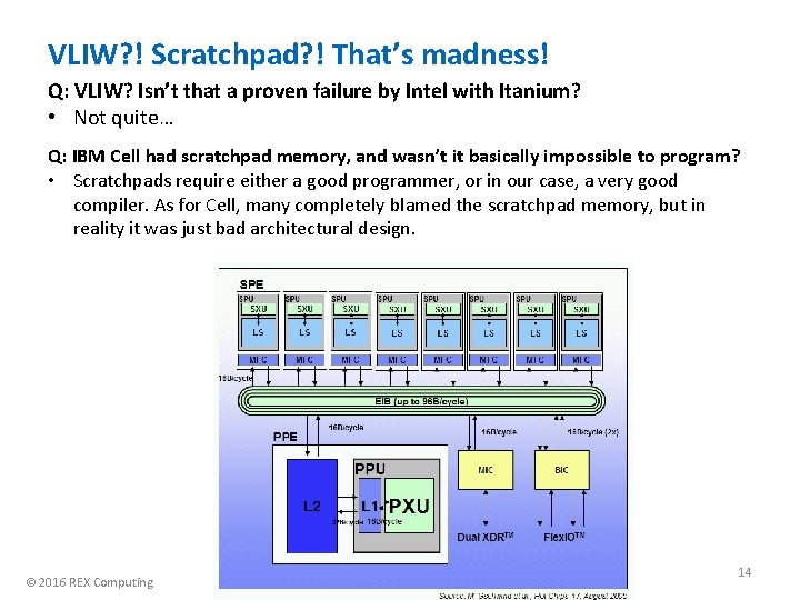
VLIW? ! Scratchpad? ! That’s madness! Q: VLIW? Isn’t that a proven failure by Intel with Itanium? • Not quite… Q: IBM Cell had scratchpad memory, and wasn’t it basically impossible to program? • Scratchpads require either a good programmer, or in our case, a very good compiler. As for Cell, many completely blamed the scratchpad memory, but in reality it was just bad architectural design. © 2016 REX Computing 14

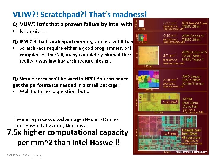
VLIW? ! Scratchpad? ! That’s madness! Q: VLIW? Isn’t that a proven failure by Intel with Itanium? • Not quite… Q: IBM Cell had scratchpad memory, and wasn’t it basically impossible to program? • Scratchpads require either a good programmer, or in our case, a very good compiler. As for Cell, many completely blamed the scratchpad memory, but in reality it was just bad architectural design. Q: Simple cores can’t be used in HPC! You can never get the performance needed in a small package! • Well that’s not a question, but… Even at a process disadvantage (Neo at 28 nm vs Intel Haswell at 22 nm), Neo has a… 7. 5 x higher computational capacity per mm^2 than Intel Haswell! © 2016 REX Computing 15

The Neo Compute Core Quad-issue VLIW Can achieve sustained theoretical peak performance for all functional units Local Scratchpad Memory Less than 0. 3 mm 2 in TSMC 28 nm © 2016 REX Computing 16

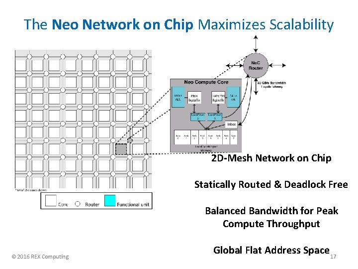
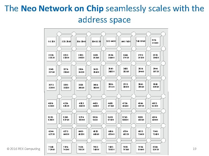
The Neo Network on Chip Maximizes Scalability 2 D-Mesh Network on Chip Statically Routed & Deadlock Free Balanced Bandwidth for Peak Compute Throughput © 2016 REX Computing Global Flat Address Space 17

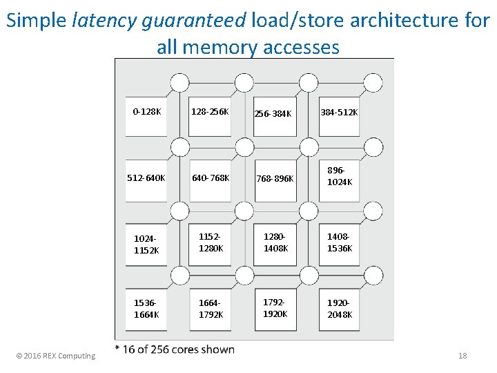
Simple latency guaranteed load/store architecture for all memory accesses © 2016 REX Computing 0 -128 K 128 -256 K 256 -384 K 384 -512 K 512 -640 K 640 -768 K 768 -896 K 8961024 K 10241152 K 11521280 K 12801408 K 14081536 K 15361664 K 16641792 K 17921920 K 19202048 K 18

The Neo Network on Chip seamlessly scales with the address space © 2016 REX Computing 0 -128 K 128 -256 K 256 -384 K 384 -512 K 512 -640 K 640 -768 K 768 -896 K 8961024 K 10241152 K 11521280 K 12801408 K 14081536 K 15361664 K 16641792 K 17921920 K 19202048 K 20482176 K 21762304 K 23042432 K 24322560 K 25602688 K 26882816 K 28162944 K 29443072 K 30723200 K 32003328 K 33283456 K 34563584 K 35843712 K 37123840 K 38403986 K 39684096 K 40964224 K 42244352 K 43524480 K 44804608 K 46084736 K 47364864 K 48644992 K 49925120 K 51205248 K 52485376 K 53765504 K 550456325760 K 57605888 K 58886016 K 60166144 K 61446272 K 62726400 K 64006528 K 65286656 K 66566784 K 67846912 K 69127040 K 70407168 K 71687296 K 72967424 K 74247552 K 75527680 K 76807808 K 78087936 K 79368064 K 80648192 K 19

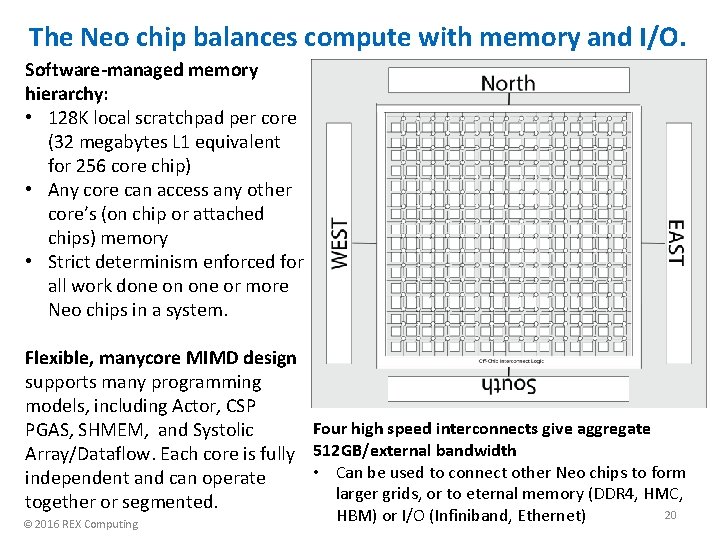
The Neo chip balances compute with memory and I/O. Software-managed memory hierarchy: • 128 K local scratchpad per core (32 megabytes L 1 equivalent for 256 core chip) • Any core can access any other core’s (on chip or attached chips) memory • Strict determinism enforced for all work done on one or more Neo chips in a system. Flexible, manycore MIMD design supports many programming models, including Actor, CSP Four high speed interconnects give aggregate PGAS, SHMEM, and Systolic Array/Dataflow. Each core is fully 512 GB/external bandwidth • Can be used to connect other Neo chips to form independent and can operate larger grids, or to eternal memory (DDR 4, HMC, together or segmented. © 2016 REX Computing HBM) or I/O (Infiniband, Ethernet) 20

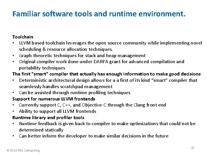
Familiar software tools and runtime environment. Toolchain • LLVM based toolchain leverages the open source community while implementing novel scheduling & resource allocation techniques. • Graph theoretic techniques for stack and heap management • Original compiler work done under DARPA grant for advanced compilation and portability techniques The first “smart” compiler that actually has enough information to make good decisions • Deterministic architectural design allows for a a first of its kind “smart” compiler that seamlessly handles scratchpad management • Can be assisted through runtime profiling techniques Support for numerous LLVM frontends • Currently support C, C++, and Objective-C through the Clang front end • Ability to support all LLVM frontends Runtime library and profiler tools • Runtime feedback is given back to compiler to make optimizations that could not be determined statically • Can better inform the developer to make similar decisions in the future © 2016 REX Computing 21

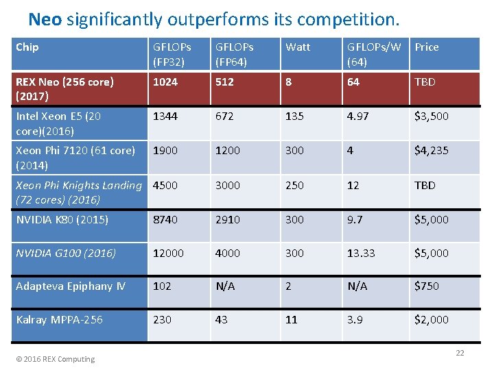
Neo significantly outperforms its competition. Chip GFLOPs (FP 32) GFLOPs (FP 64) Watt GFLOPs/W (64) Price REX Neo (256 core) (2017) 1024 512 8 64 TBD Intel Xeon E 5 (20 core)(2016) 1344 672 135 4. 97 $3, 500 Xeon Phi 7120 (61 core) (2014) 1900 1200 300 4 $4, 235 Xeon Phi Knights Landing 4500 (72 cores) (2016) 3000 250 12 TBD NVIDIA K 80 (2015) 8740 2910 300 9. 7 $5, 000 NVIDIA G 100 (2016) 12000 4000 300 13. 33 $5, 000 Adapteva Epiphany IV 102 N/A $750 Kalray MPPA-256 230 43 11 3. 9 $2, 000 © 2016 REX Computing 22

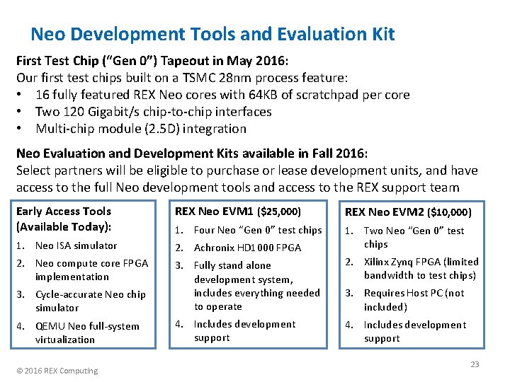
Neo Development Tools and Evaluation Kit First Test Chip (“Gen 0”) Tapeout in May 2016: Our first test chips built on a TSMC 28 nm process feature: • 16 fully featured REX Neo cores with 64 KB of scratchpad per core • Two 120 Gigabit/s chip-to-chip interfaces • Multi-chip module (2. 5 D) integration Neo Evaluation and Development Kits available in Fall 2016: Select partners will be eligible to purchase or lease development units, and have access to the full Neo development tools and access to the REX support team Early Access Tools (Available Today): REX Neo EVM 1 ($25, 000) REX Neo EVM 2 ($10, 000) 1. Four Neo “Gen 0” test chips 1. Neo ISA simulator 2. Achronix HD 1000 FPGA 1. Two Neo “Gen 0” test chips 2. Neo compute core FPGA implementation 2. Xilinx Zynq FPGA (limited bandwidth to test chips) 3. Cycle-accurate Neo chip simulator 3. Fully stand alone development system, includes everything needed to operate 3. Requires Host PC (not included) 4. QEMU Neo full-system virtualization 4. Includes development support © 2016 REX Computing 23

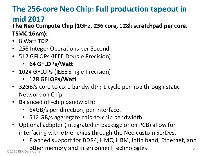
The 256 -core Neo Chip: Full production tapeout in mid 2017 The Neo Compute Chip (1 GHz, 256 core, 128 k scratchpad per core, TSMC 16 nm): • 8 Watt TDP • 256 Integer Operations per Second • 512 GFLOPs (IEEE Double Precision) • 64 GFLOPs/Watt • 1024 GFLOPs (IEEE Single Precision) • 128 GFLOPs/Watt • 32 GB/s core to core bandwidth; 1 cycle per hop through static Network on Chip • Balanced off-chip bandwidth: • 64 GB/s per direction, per interface. • 512 GB/s aggregate chip-to-chip bandwidth • Optional adapter (integrated in package or on PCB) allow for interfacing with other chips through the Neo custom Ser. Des. • Planned support for DDR 4, HMC, HBM, Infiniband, Ethernet, and other memory and interconnect technologies 24 © 2016 REX Computing

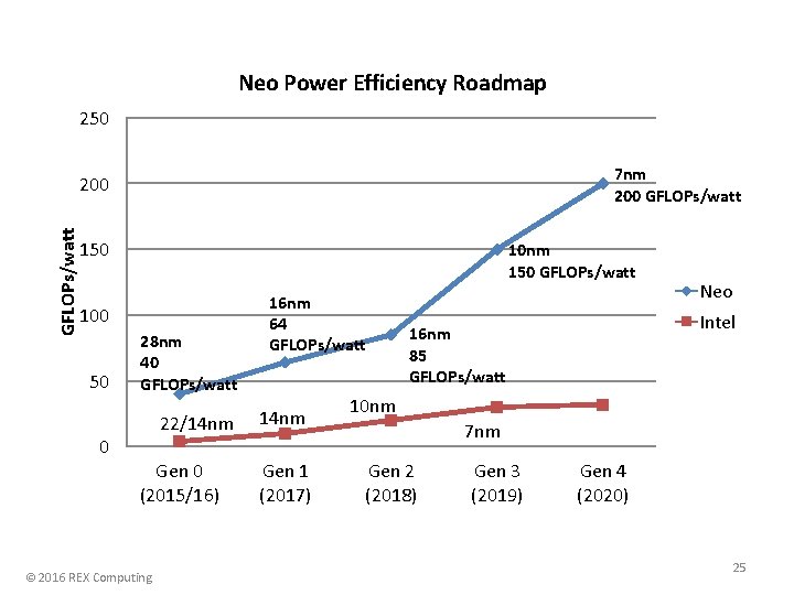
Neo Power Efficiency Roadmap 250 7 nm 200 GFLOPs/watt 200 150 10 nm 150 GFLOPs/watt 100 50 0 28 nm 40 GFLOPs/watt 22/14 nm Gen 0 (2015/16) © 2016 REX Computing 16 nm 64 GFLOPs/watt 14 nm Gen 1 (2017) Neo Intel 16 nm 85 GFLOPs/watt 10 nm 7 nm Gen 2 (2018) Gen 3 (2019) Gen 4 (2020) 25

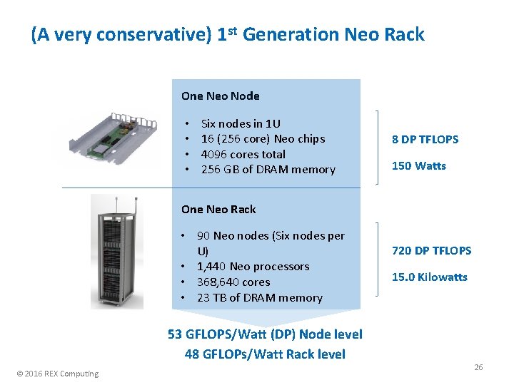
(A very conservative) 1 st Generation Neo Rack One Neo Node • • Six nodes in 1 U 16 (256 core) Neo chips 4096 cores total 256 GB of DRAM memory 8 DP TFLOPS 150 Watts One Neo Rack • 90 Neo nodes (Six nodes per U) • 1, 440 Neo processors • 368, 640 cores • 23 TB of DRAM memory 53 GFLOPS/Watt (DP) Node level 48 GFLOPs/Watt Rack level © 2016 REX Computing 720 DP TFLOPS 15. 0 Kilowatts 26

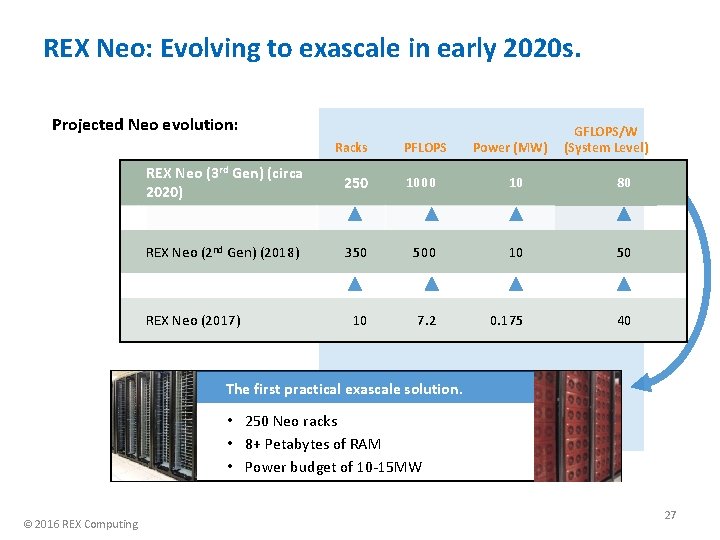
REX Neo: Evolving to exascale in early 2020 s. Projected Neo evolution: Racks PFLOPS Power (MW) GFLOPS/W (System Level) REX Neo (3 rd Gen) (circa 2020) 250 1000 10 80 REX Neo (2 nd Gen) (2018) 350 500 10 50 10 7. 2 0. 175 40 REX Neo (2017) The first practical exascale solution. • 250 Neo racks • 8+ Petabytes of RAM • Power budget of 10 -15 MW © 2016 REX Computing 27

The REX Neo: A New Processor Architecture for Exascale and Beyond Thomas Sohmers March 24 th 2016 SOS 20