The Prompt Trigger of the Silicon Pixel Detector

- Slides: 1

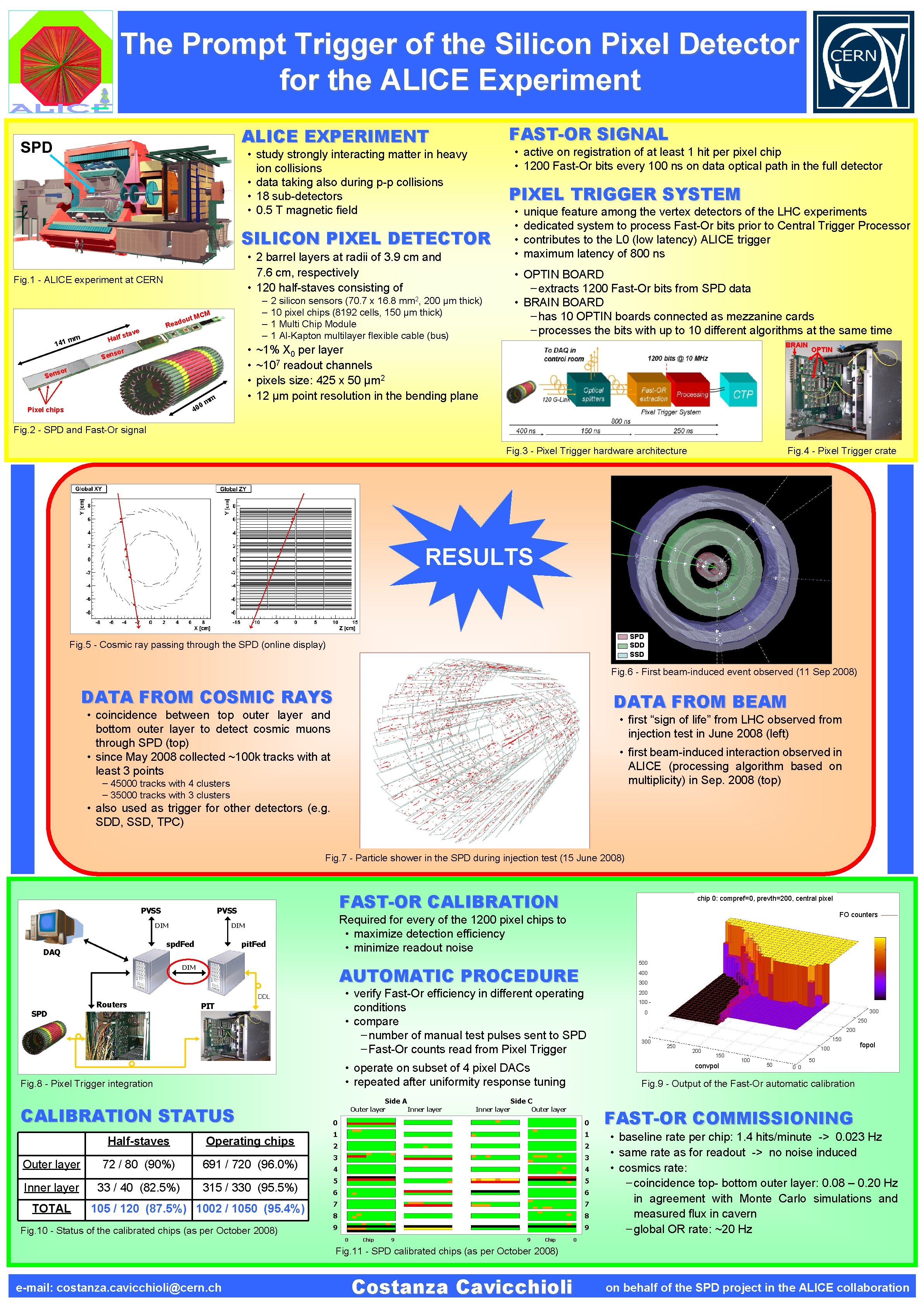
The Prompt Trigger of the Silicon Pixel Detector for the ALICE Experiment FAST-OR SIGNAL ALICE EXPERIMENT SPD • active on registration of at least 1 hit per pixel chip • 1200 Fast-Or bits every 100 ns on data optical path in the full detector • study strongly interacting matter in heavy ion collisions • data taking also during p-p collisions • 18 sub-detectors • 0. 5 T magnetic field PIXEL TRIGGER SYSTEM • • SILICON PIXEL DETECTOR • 2 barrel layers at radii of 3. 9 cm and 7. 6 cm, respectively • 120 half-staves consisting of Fig. 1 - ALICE experiment at CERN – – M MC t u o mm 1 4 1 d Rea ave t s f Hal • • or s n Se sor n e S m m 0 unique feature among the vertex detectors of the LHC experiments dedicated system to process Fast-Or bits prior to Central Trigger Processor contributes to the L 0 (low latency) ALICE trigger maximum latency of 800 ns • OPTIN BOARD −extracts 1200 Fast-Or bits from SPD data • BRAIN BOARD −has 10 OPTIN boards connected as mezzanine cards −processes the bits with up to 10 different algorithms at the same time 2 silicon sensors (70. 7 x 16. 8 mm 2, 200 μm thick) 10 pixel chips (8192 cells, 150 μm thick) 1 Multi Chip Module 1 Al-Kapton multilayer flexible cable (bus) BRAIN ~1% X 0 per layer ~107 readout channels pixels size: 425 x 50 μm 2 12 μm point resolution in the bending plane OPTIN 40 Pixel chips Fig. 2 - SPD and Fast-Or signal Fig. 3 - Pixel Trigger hardware architecture Fig. 4 - Pixel Trigger crate RESULTS SPD SDD SSD Fig. 5 - Cosmic ray passing through the SPD (online display) Fig. 6 - First beam-induced event observed (11 Sep 2008) DATA FROM COSMIC RAYS DATA FROM BEAM • coincidence between top outer layer and bottom outer layer to detect cosmic muons through SPD (top) • since May 2008 collected ~100 k tracks with at least 3 points • first “sign of life” from LHC observed from injection test in June 2008 (left) • first beam-induced interaction observed in ALICE (processing algorithm based on multiplicity) in Sep. 2008 (top) − 45000 tracks with 4 clusters − 35000 tracks with 3 clusters • also used as trigger for other detectors (e. g. SDD, SSD, TPC) Fig. 7 - Particle shower in the SPD during injection test (15 June 2008) PVSS DIM pit. Fed SPD PIT Inner layer TOTAL 72 / 80 (90%) 33 / 40 (82. 5%) 300 • operate on subset of 4 pixel DACs • repeated after uniformity response tuning CALIBRATION STATUS Outer layer 400 • verify Fast-Or efficiency in different operating conditions • compare −number of manual test pulses sent to SPD −Fast-Or counts read from Pixel Trigger DDL Fig. 8 - Pixel Trigger integration Half-staves 500 AUTOMATIC PROCEDURE DIM Routers FO counters Required for every of the 1200 pixel chips to • maximize detection efficiency • minimize readout noise DIM spd. Fed DAQ FAST-OR CALIBRATION PVSS chip 0: compref=0, prevth=200, central pixel Operating chips 691 / 720 (96. 0%) 315 / 330 (95. 5%) 105 / 120 (87. 5%) 1002 / 1050 (95. 4%) Fig. 10 - Status of the calibrated chips (as per October 2008) Side A Outer layer 250 200 300 150 200 150 100 50 fopol 50 0 0 Side C Inner layer Outer layer 1 1 2 2 3 3 4 4 5 5 6 6 7 7 8 8 9 9 9 300 0 Fig. 9 - Output of the Fast-Or automatic calibration 0 Chip 100 convpol 0 0 200 9 Chip FAST-OR COMMISSIONING • baseline rate per chip: 1. 4 hits/minute -> 0. 023 Hz • same rate as for readout -> no noise induced • cosmics rate: −coincidence top- bottom outer layer: 0. 08 – 0. 20 Hz in agreement with Monte Carlo simulations and measured flux in cavern −global OR rate: ~20 Hz 0 Fig. 11 - SPD calibrated chips (as per October 2008) e-mail: costanza. cavicchioli@cern. ch Costanza Cavicchioli on behalf of the SPD project in the ALICE collaboration