The Processor Lecture 3 1 Introduction Logic Design
- Slides: 12

The Processor Lecture 3. 1: Introduction & Logic Design Conventions 1

Learning Objectives q Describe the steps in the generic implementation of the processor q Explain what ALU (arithmetic logic unit) does for each of 9 instructions q Define the basic behavior of registers q Understand the edge-triggered methodology 2

Coverage q Chapter 4. 1: Introduction q Chapter 4. 2: Logic Design Conventions 3

q Introduction l Chapter 4. 1 4

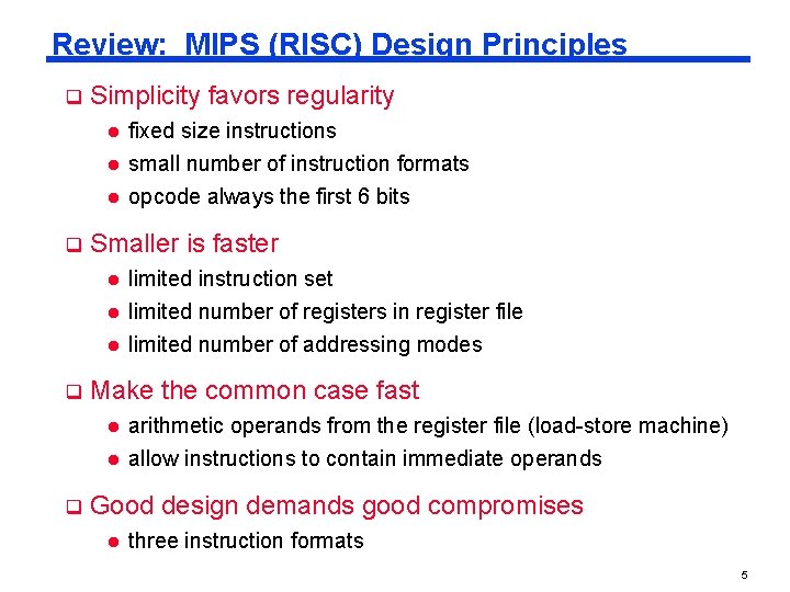
Review: MIPS (RISC) Design Principles q Simplicity favors regularity l l l q q Smaller is faster l limited instruction set l limited number of registers in register file l limited number of addressing modes Make the common case fast l l q fixed size instructions small number of instruction formats opcode always the first 6 bits arithmetic operands from the register file (load-store machine) allow instructions to contain immediate operands Good design demands good compromises l three instruction formats 5

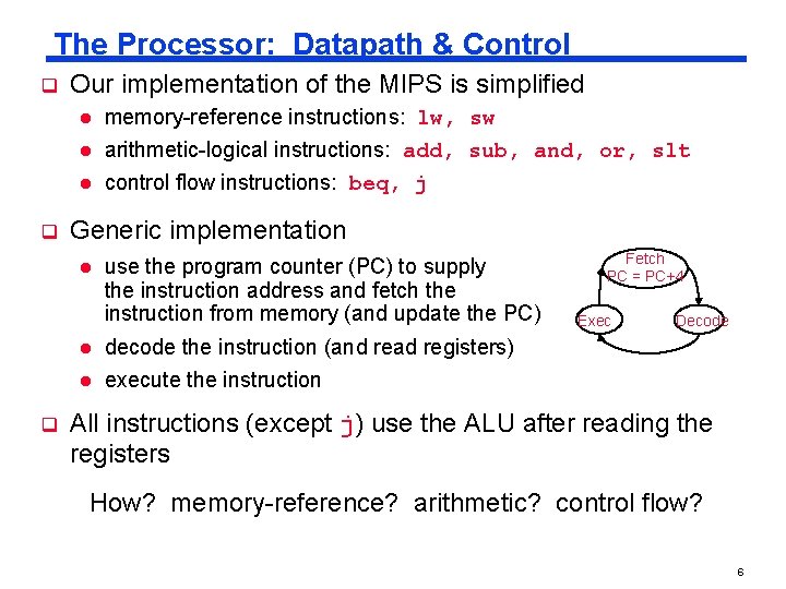
The Processor: Datapath & Control q Our implementation of the MIPS is simplified l l l q Generic implementation l l l q memory-reference instructions: lw, sw arithmetic-logical instructions: add, sub, and, or, slt control flow instructions: beq, j use the program counter (PC) to supply the instruction address and fetch the instruction from memory (and update the PC) Fetch PC = PC+4 Exec Decode decode the instruction (and read registers) execute the instruction All instructions (except j) use the ALU after reading the registers How? memory-reference? arithmetic? control flow? 6

q Logic Design Conventions l Chapter 4. 2 7

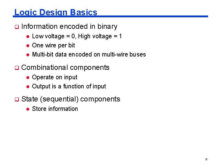
Logic Design Basics q Information encoded in binary l l l q q Low voltage = 0, High voltage = 1 One wire per bit Multi-bit data encoded on multi-wire buses Combinational components l Operate on input l Output is a function of input State (sequential) components l Store information 8

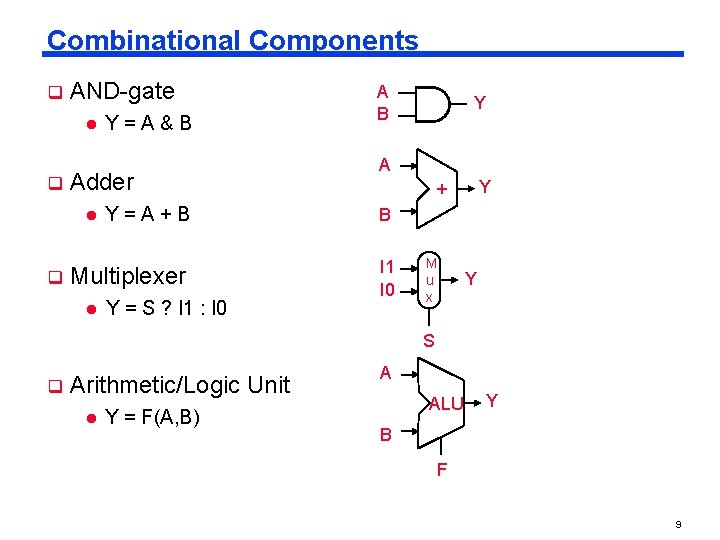
Combinational Components q AND-gate l q Adder Multiplexer I 1 I 0 Y = S ? I 1 : I 0 Y + B l Y A Y=A+B l q Y=A&B A B M u x Y S q Arithmetic/Logic Unit l Y = F(A, B) A ALU Y B F 9

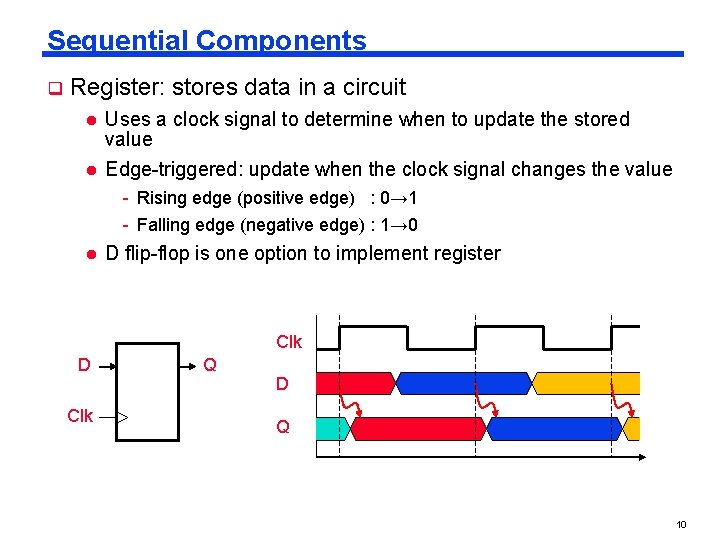
Sequential Components q Register: stores data in a circuit l l Uses a clock signal to determine when to update the stored value Edge-triggered: update when the clock signal changes the value - Rising edge (positive edge) : 0→ 1 - Falling edge (negative edge) : 1→ 0 l D flip-flop is one option to implement register Clk D Clk Q D Q 10

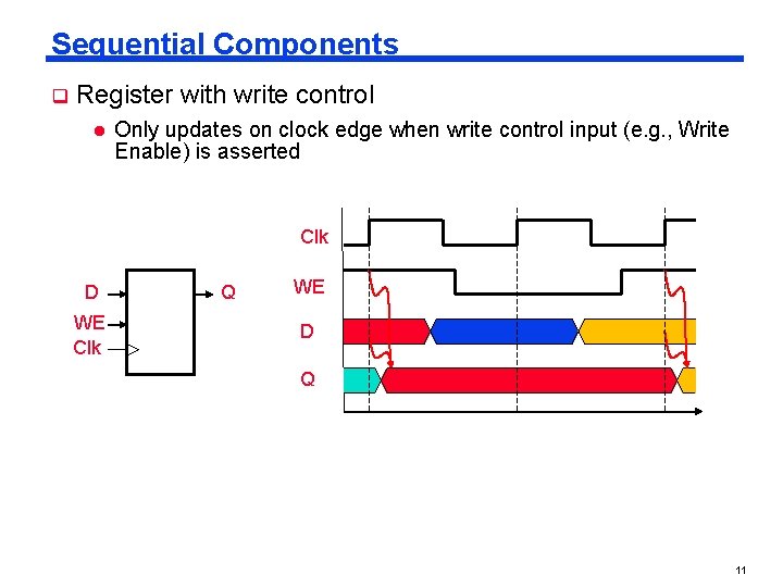
Sequential Components q Register with write control l Only updates on clock edge when write control input (e. g. , Write Enable) is asserted Clk D WE Clk Q WE D Q 11

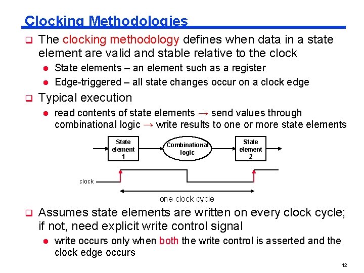
Clocking Methodologies q The clocking methodology defines when data in a state element are valid and stable relative to the clock l l q State elements – an element such as a register Edge-triggered – all state changes occur on a clock edge Typical execution l read contents of state elements → send values through combinational logic → write results to one or more state elements State element 1 Combinational logic State element 2 clock one clock cycle q Assumes state elements are written on every clock cycle; if not, need explicit write control signal l write occurs only when both the write control is asserted and the clock edge occurs 12