The pn Junction COURSE OBJECTIVE Description about pn

The pn Junction

COURSE OBJECTIVE � � Description about pn Junction Diode Briefing about N-type & p-Type Forward-Biased pn Junction Reverse-Biased pn Junction

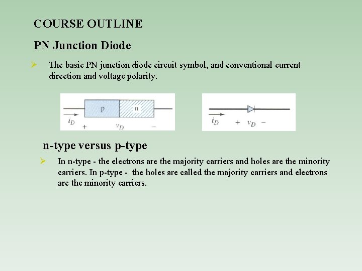
COURSE OUTLINE PN Junction Diode Ø The basic PN junction diode circuit symbol, and conventional current direction and voltage polarity. n-type versus p-type Ø In n-type - the electrons are the majority carriers and holes are the minority carriers. In p-type - the holes are called the majority carriers and electrons are the minority carriers.

Reverse-Biased pn Junction Ø +ve terminal is applied to the n-region of the pn junction and vice versa. Ø Applied voltage VR will induce an applied electric field EA. Ø Magnitude of the electric field in the space-charge region increases above thermal equilibrium value. Total ET = E + EA Ø Increased electric field holds back the holes in the p-region and the electrons in the n-region. Ø Hence, no current across the pn junction. Ø This applied voltage polarity is called reverse bias. Forward-Biased pn Junction Ø +ve terminal is applied to the p-region of the pn junction and vice versa. Ø Direction of the applied electric field EA is the opposite as that of the E-field in the space-charge region. Ø The net result is that the electric field in the space-charge region lower than thermal equilibrium value causing diffusion of charges to begin again. Ø The diffusion process continues as long as VD is applied.

Assessment Strategy � � Exercise Sheets Multiple Choice Questions Design Consideration 1. 2. 3. Font Size Allignment Colour
- Slides: 5