The physics of blue lasers solar cells and

The physics of blue lasers, solar cells, and stop lights Paul Kent University of Cincinnati & ORNL

The physics of blue lasers, solar cells, and stop lights Paul Kent Solid State Theory Group National Renewable Energy Laboratory Thanks to: Alex Zunger & SST Group/Basic Sciences U. S. Department of Energy Office of Science Basic Energy Sciences Division of Materials Sciences

Outline 1. Introduction Nitride semiconductors Novel phenomena. Localized states 2. How can we model these systems? Computational techniques 3. New photovoltaic materials Ga. As. N (and Ga. PN) Band gap reduction. Localized states 4. Blue emitters In. Ga. N Localization at In inhomogeneities

Blue laser Sony 30 GB DVD High brightness LEDs Traffic signals. Solid state lighting? In. Ga. N, Al. Ga. N… In. Ga. N Ga. As/Ge 19% eff. High efficiency photovoltaics? Ga. As. N
")
Absorption in semiconductors Energy Conduction band Photon hn Valance band (occupied states)

High Efficiency Multijunction Solar Cells • Want 1 e. V material latticematched to Ga. As Þ Try Ga. In. NAs Calculated efficiencies (ideal) 500 X AM 1. 5 D: 36% 47% one sun AM 0: 31% 38% 52% 41%

Isostructural semiconductor alloying Properties approx. a linear combination of the components

No ni tro ge n Anomaly #1: Band gap reduction in Ga. As. N 0. 9 % 1. 2 % 2% Band gaps Ga. As ~1. 5 e. V Ga. N ~3. 5 e. V Shan et al. Phys. Rev. Lett. 82 1221 (1999) Band gap reduced by ~120 me. V per % nitrogen!

Anomaly #2: Dilute Nitrogen in Ga. As: N NN 1 1 kbar 0 kbar Wavelength (nm) Liu, Pistol and Samuelson. Appl. Phys. Lett. 56 1451 (1990) T. Makimoto et al. Appl. Phys. Lett. 70 2984 (1997) Many sharp lines seen in emission!

Outline 1. Introduction Nitride semiconductors Novel phenomena. Localized states 2. How can we model these systems? Computational techniques 3. New photovoltaic materials Ga. As. N (and Ga. PN) Band gap reduction. Localized states 4. Blue emitters In. Ga. N Localization at In inhomogeneities

Simplified view of a semiconductor alloy Simulate regular lattices Distributions of atoms 10^3 -10^6 atoms required Atomic relaxation important

Computational Modeling of Alloys Small Supercell Approach Large Supercell Approach Use large supercells (10^3 -10^6 atoms) containing many nitrogens Statistically average properties of many random configurations Use Valence Force Field for structural relaxation Use Empirical Pseudopotential Method for wavefunctions
 5 4 conduction 3 states 2 1 Band Gap N")
Folded Spectrum Method (FSM) 5 4 conduction 3 states 2 1 Band Gap N N-1 valence N-2 states N-3 N-4 conduction states valence states 5 4 3 2 1 eref “Fold” States Only calculate “interesting” states around band gap 1 Wang & Zunger J. Chem. Phys. (1994) Recently: Jacobi-Javidson Tackett PRB (2002)

Outline 1. Introduction Nitride semiconductors Novel phenomena. Localized states 2. How can we model these systems? Computational techniques 3. New photovoltaic materials Ga. As. N (and Ga. PN) Band gap reduction. Localized states 4. Blue emitters In. Ga. N Localization at In inhomogeneities

High Efficiency Multijunction Solar Cells • Want 1 e. V material latticematched to Ga. As ÞTry Ga. In. NAs Calculated efficiencies (ideal) 500 X AM 1. 5 D: 36% 47% one sun AM 0: 31% 38% 52% 41%

No ni tro ge n Anomaly #1: Band gap reduction in Ga. As. N 0. 9 % 1. 2 % 2% Band gaps Ga. As ~1. 5 e. V Ga. N ~3. 5 e. V Shan et al. Phys. Rev. Lett. 82 1221 (1999) Band gap reduced by ~120 me. V per % nitrogen!

Anomaly #2: Dilute Nitrogen in Ga. As: N NN 1 1 kbar 0 kbar Wavelength (nm) Liu, Pistol and Samuelson. Appl. Phys. Lett. 56 1451 (1990) T. Makimoto et al. Appl. Phys. Lett. 70 2984 (1997) Many sharp lines seen in emission!

N in Ga. As, Ga. P I will discuss three cases: 1. Isolated Nitrogen 2. Pairs and clusters 3. Well-developed alloys
: Level ~30 me. V below")
Ga. P: N In Ga. P: N (0. 01%): Level ~30 me. V below CBM Introduces G character Any concentration of nitrogen in Ga. P creates “direct gap” character Nitrogen localized a 1(N)

A 1 Levels of Isolated Impurity Ga. As: N Localized Level in Ga. As: N rom 44 44 Angs t An gst rom G / L / X (%) 4096 atoms Nitrogen localized level ~ 150 me. V inside conduction band

N in Ga. As, Ga. P 1. Isolated Nitrogen 2. Pairs and clusters 3. Well-developed alloys
 Clusters 2")
N Clusters in Ga. As, Ga. P 1. Ga(Pm. N 4 -m) Clusters 2 N 1 N 3 N 4 N 2. [1, 1, 0]-Oriented Nitrogen Chains [1, 1, 0] N N N

Energy levels of Clusters and Chains in Ga. P

N in Ga. As, Ga. P 1. Isolated Nitrogen 2. Pairs and clusters 3. Well-developed alloys

ECBE = Delocalized Conduction Band Edge
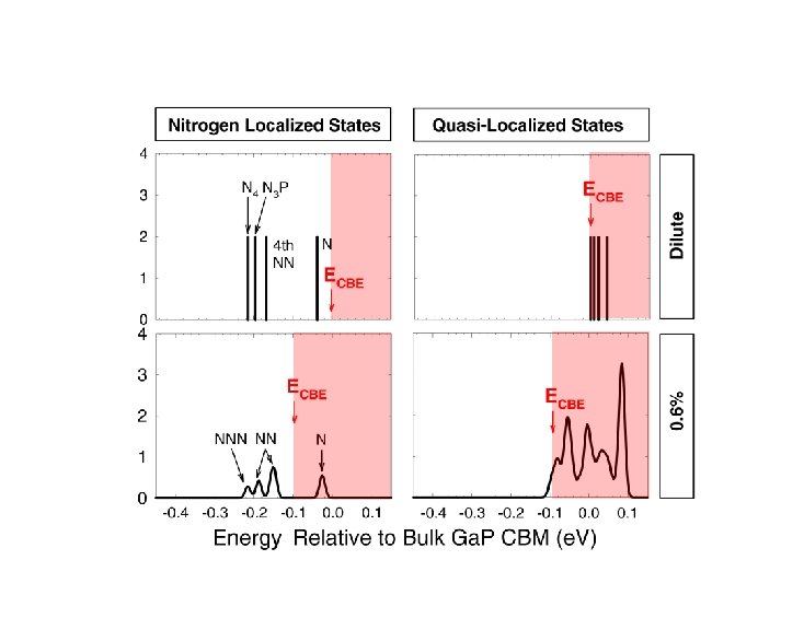

Ga. PN

Ga. As. N

Two types of state observed Dilute Limit: PHS in conduction band pair/cluster CS in gap Intermediate Range: CS do not move PHS plunge down in energy Amalgamation Point: Lowest energy PHS just below CS

Band gap reduction Anticrossing/repulsion between band edge and localized states drives band gap down

Ga. PN Pressure dependence Energy Bulk Ga. P – 14 me. V/GPa Pressure

Red Shift of PL vs PLE Majority state absorbs Minority state emits I. A. Buyanova et al. MRS IJNSR 6 2 (2001) - Emission from localized minority states - Absorption to majority states

Summary: Ga. As. N & Ga. PN 1. Small nitrogen aggregates create near-gap levels Some “cluster state” levels are deep, even for small aggregates 2. Cluster states are fixed in energy 3. Host states move down, overtaking the cluster levels, one-by-one Host states repelled from nitrogen resonant levels 4. Both localized and delocalized states exist at the band edge Kent & Zunger Phys. Rev. Lett. 86 2613 (2001) Kent & Zunger Phys. Rev. B 64 5208 (2001) Kent & Zunger Appl. Phys. Lett. 79 2339( 2001)

Outline 1. Introduction Nitride semiconductors Novel phenomena. Localized states 2. How can we model these systems? Computational techniques 3. New photovoltaic materials Ga. As. N (and Ga. PN) Band gap reduction. Localized states 4. Blue emitters In. Ga. N Localization at In inhomogeneities

Zinc-Blende In. Ga. N Alloys Why is emission so efficient? Despite large defect density In. Ga. N alloys emit • Time resolved PL – many length (time) scales • Theory: Bulk In. Ga. N alloys emit weakly Q. What is the role of In inhomogeneity?

In. Ga. N band offsets
 10")
Experimental Observations 15% In 20% In Lemos et al. PRL 84 3666 (2000) 10 nm 25% In HRTEM In. Ga. N MQW Lin et al. APL 77 2988 (2000) ~300 me. V+ lowering in emission energy in 33% c-In. Ga. N samples

In. Ga. N Intrinsic Dot Calculations Spherical dot in 141000 atom supercell Dot: High In composition 80%+ Alloy supercell: Lower In composition 33% Electrons Quantum confined on dot Holes Localized in/near dot (strain, alloy fluctuations)

Calculations of Intrinsic Dots Small In-rich regions give large “band gap” reduction

Hole Localization in Random Alloys 1000 atom supercell 20% In Holes localize near (statistically occurring) (1, 1, 0)-oriented Indium chains!

Indium fluctuations are key } “Quantum dot” states due to inhomogeneity Localized states occur near VBM, CBM

Summary: In. Ga. N Indium fluctuations are key - localization easily results => Can specify quality of growth required for opto devices • Small (~30 A) In-rich (80%+) regions cause low energy PL • Localized hole states exist even in random alloy Kent & Zunger Appl. Phys. Lett. 79 1977 (2001)

Conclusion 1. Nitride alloys display “new physics” due to formation of localized states 2. Large-scale computational modeling can help explain nitride properties prc. kent@physics. org http: //www. physics. uc. edu/~pkent
- Slides: 44