
The PGL Nanoruler Scans a Small Beam of
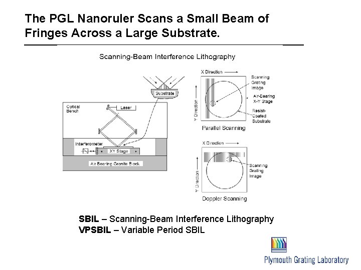
The PGL Nanoruler Scans a Small Beam of Fringes Across a Large Substrate. SBIL – Scanning-Beam Interference Lithography VPSBIL – Variable Period SBIL
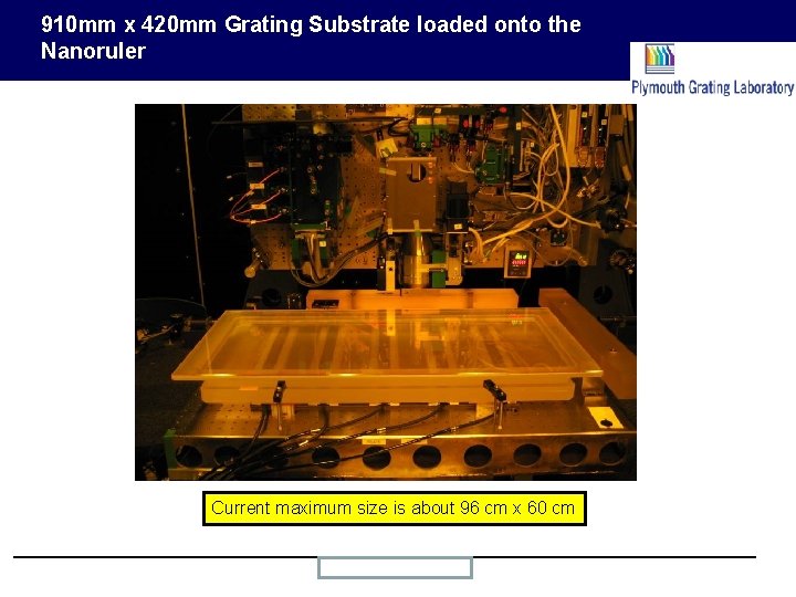
910 mm x 420 mm Grating Substrate loaded onto the Nanoruler Current maximum size is about 96 cm x 60 cm PGL Proprietary Information
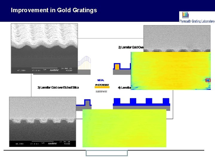
Improvement in Gold Gratings PGL Proprietary Information
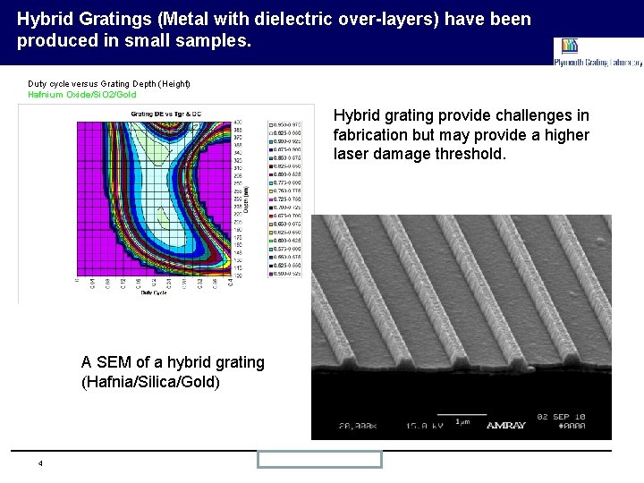
Hybrid Gratings (Metal with dielectric over-layers) have been produced in small samples. Duty cycle versus Grating Depth (Height) Hafnium Oxide/Si. O 2/Gold Hybrid grating provide challenges in fabrication but may provide a higher laser damage threshold. A SEM of a hybrid grating (Hafnia/Silica/Gold) 4 PGL Proprietary Information
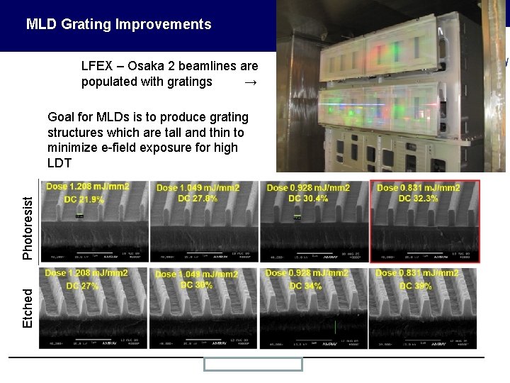
MLD Grating Improvements LFEX – Osaka 2 beamlines are populated with gratings → Etched Photoresist Goal for MLDs is to produce grating structures which are tall and thin to minimize e-field exposure for high LDT PGL Proprietary Information
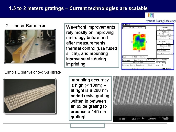
1. 5 to 2 meters gratings – Current technologies are scalable 2 – meter Bar mirror Wavefront improvements rely mostly on improving metrology before and after measurements, thermal control (use fused silica!), and mounting inprovements during imprinting. Simple Light-weighted Substrate Imprinting accuracy is high (< 10 nm) – at right is a 280 nm period resist grating written in between an oxide grating to produce a 140 nm grating! PGL Proprietary Information
- Slides: 6