The PERCIVAL CMOS Image Sensor Pixelated Energy Resolving






- Slides: 30

The PERCIVAL CMOS Image Sensor Pixelated Energy Resolving CMOS Imager Versatile and Large Iain Sedgwick STFC – Rutherford Appleton Laboratory iain. sedgwick@stfc. ac. uk www. dsc. stfc. ac. uk/cmossensors

INTRODUCTION PERCIVAL – Pixelated Energy Resolving CMOS Imager, Versatile and Large • Develop a wafer scale, high frame rate CMOS imager for low energy X-Ray detection • Work undertaken at four sites • • Rutherford Appleton Laboratory – Sensor Design and Testing DESY – Electronics and Testing Elettra – Electronics and Software • 1 Diamond Light Source – DAQ • All devices use the Tower. Jazz 0. 18 um process • Backthinning carried out under contract with the NASA Jet Propulsion Laboratory (JPL) 2

THE TEAM Deutsches Elektronen-Synchrotron (DESY) Matthias Bayer, Jonathan Correa, Peter Gottlicher, Heinz Graafsma, Sabine Lange, Helmut Hirsemann, Alessandro Marras, Igor Shevyakov, Sergej Smoljanin, Michele Viti, Cornelia Wunderer, Qingqing Xia, Manfred Zimmer Diamond Light Source (DLS) Julien Marchal, Tim Nicholls, Ulrik Pedersen, Nick Rees, Nicola Tartoni, Jonathon Thompson Elettra – Sincrotrone Trieste (Elettra) Giuseppe Cautero, Dario Giuressi, Ralf Menk, Luigi Stebel, Hazem Yousef Rutherford Appleton Laboratory (STFC – RAL) Dipayan Das, Nicola Guerrini, Ben Marsh, Iain Sedgwick, Renato Turchetta 3

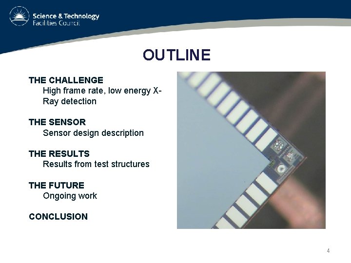
OUTLINE THE CHALLENGE High frame rate, low energy XRay detection THE SENSOR Sensor design description THE RESULTS Results from test structures • 1 THE FUTURE Ongoing work CONCLUSION 4

THE CHALLENGE

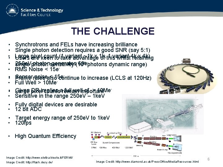
THE CHALLENGE • • • Synchrotrons and FELs have increasing brilliance Single photon detection requires a good SNR (say 5: 1) Large count variant ~1 k x 1 k, 1 variant x 4 k) Users pixel are keen to(1 take advantage of this whilst 4 k retaining 5 -photons dynamic range) 250 e. Vphotonsensitivity generates(10 69 e single RMS Noise < 15 e. Sensorrates noisealso < 15 e Frame continue to increase (LCLS at 120 Hz) Full Well > 10 Me Given pixel DR implies full wellimportant of > 10 Me. Large countsaremain Sensitive in the range 250 e. V – 1 ke. V • Fully digital devices are desirable • 12 bit ADC • Target energy range of 250 e. V to 1 ke. V • 120 fps • High Quantum Efficiency Image Credit: http: //www. elettra. trieste. it/FERMI/ Image Credit: http: //flash. desy. de/ Image Credit: http: //www. diamond. ac. uk/Press. Office/Media. Resources. html 6

THE SENSOR

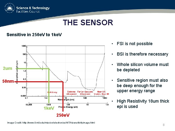
THE SENSOR Sensitive in 250 e. V to 1 ke. V • FSI is not possible • BSI is therefore necessary • Whole silicon volume must be depleted 2 um • Sensitive region must also be deep enough for the upper energy range 50 nm • High Resistivity 18 um thick epi is used 1 ke. V 250 e. V Image Credit: http: //www. ll. mit. edu/mission/electronics/AIT/hisensitivityimage. html 8

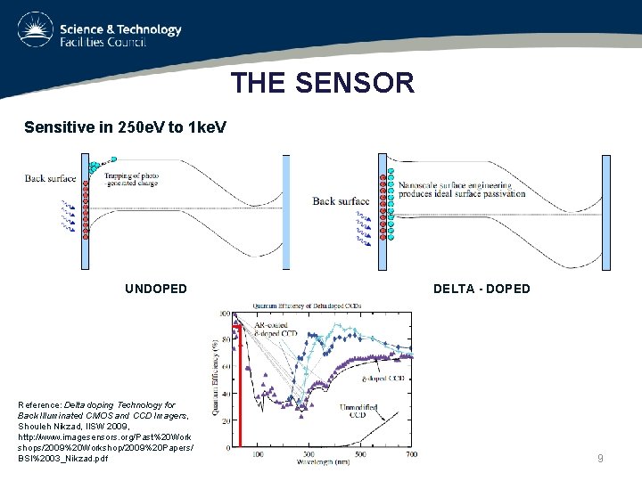
THE SENSOR Sensitive in 250 e. V to 1 ke. V UNDOPED Reference: Delta doping Technology for Back Illuminated CMOS and CCD Imagers, Shouleh Nikzad, IISW 2009, http: //www. imagesensors. org/Past%20 Work shops/2009%20 Workshop/2009%20 Papers/ BSI%2003_Nikzad. pdf DELTA - DOPED 9

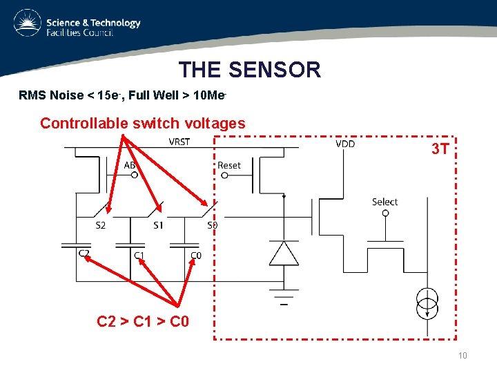
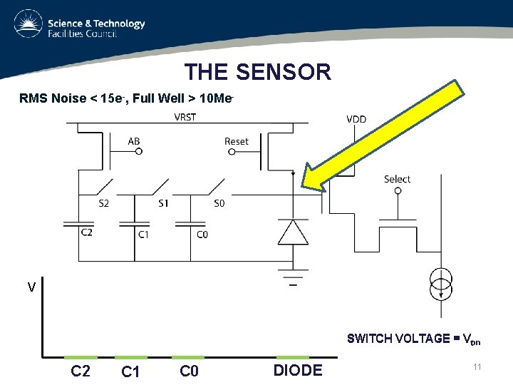
THE SENSOR RMS Noise < 15 e-, Full Well > 10 Me- Controllable switch voltages 3 T C 2 > C 1 > C 0 10

THE SENSOR RMS Noise < 15 e-, Full Well > 10 Me- V SWITCH VOLTAGE = Vton C 2 C 1 C 0 DIODE 11

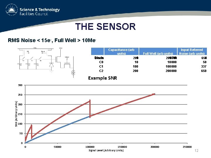
THE SENSOR RMS Noise < 15 e-, Full Well > 10 Me. Diode C 0 C 1 C 2 Capacitance (arb units) 1 200 10 100 200 Input Referred Full Well (arb units) Noise (arb units) 1000 4 200000 650 100000 337 200000 650 Example SNR 300 SNR (Arbitrary Units) 250 200 150 100 50 0 0 50000 100000 150000 Signal Level (Arbitrary Units) 200000 250000 12

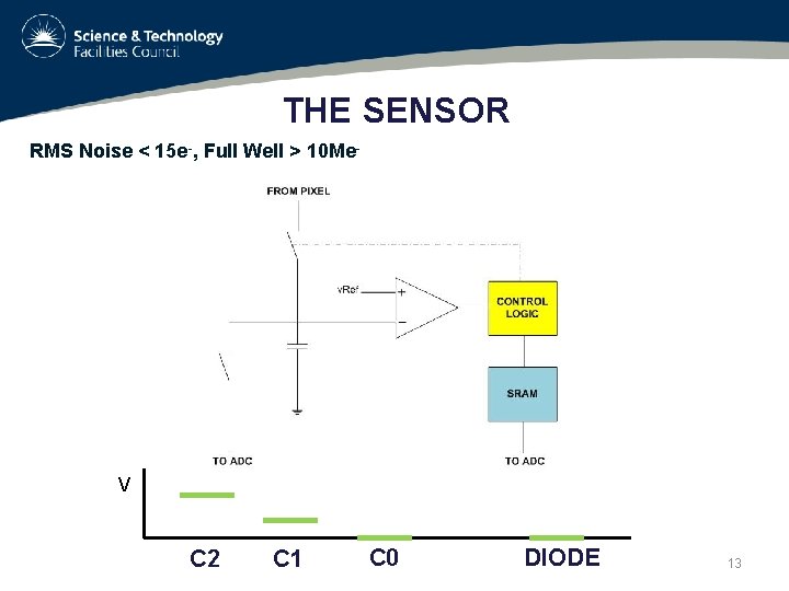
THE SENSOR RMS Noise < 15 e-, Full Well > 10 Me- V C 2 C 1 C 0 DIODE 13

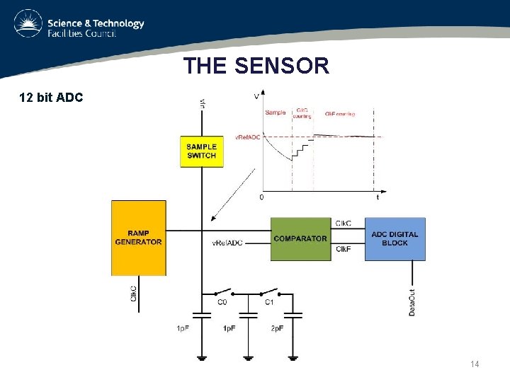
THE SENSOR 12 bit ADC 14

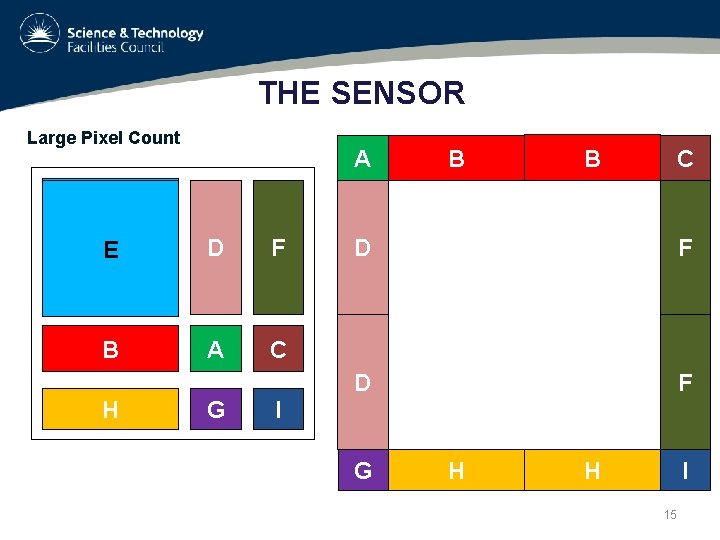
THE SENSOR Large Pixel Count A E D F B A C H G B B C D F I G H H I 15

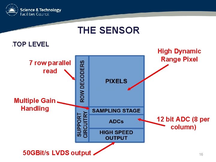
THE SENSOR l TOP LEVEL 7 row parallel read High Dynamic Range Pixel Multiple Gain Handling 12 bit ADC (8 per column) 50 GBit/s LVDS output 16

THE RESULTS

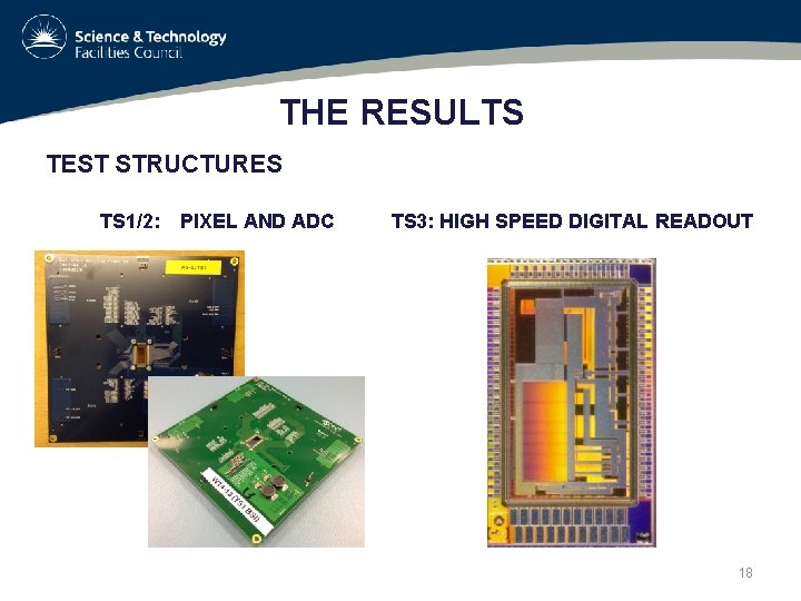
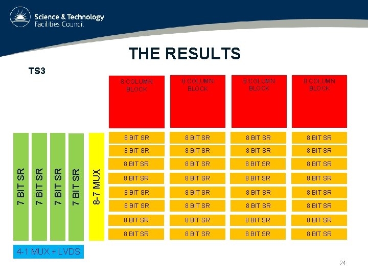
THE RESULTS TEST STRUCTURES TS 1/2: PIXEL AND ADC TS 3: HIGH SPEED DIGITAL READOUT 18

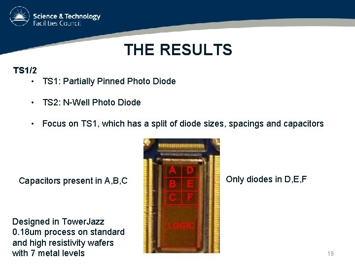
THE RESULTS TS 1/2 • TS 1: Partially Pinned Photo Diode • TS 2: N-Well Photo Diode • Focus on TS 1, which has a split of diode sizes, spacings and capacitors Capacitors present in A, B, C Designed in Tower. Jazz 0. 18 um process on standard and high resistivity wafers with 7 metal levels Only diodes in D, E, F 19

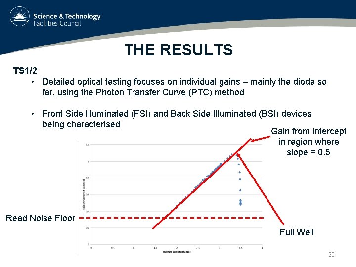
THE RESULTS TS 1/2 • Detailed optical testing focuses on individual gains – mainly the diode so far, using the Photon Transfer Curve (PTC) method • Front Side Illuminated (FSI) and Back Side Illuminated (BSI) devices being characterised Gain from intercept in region where slope = 0. 5 Read Noise Floor Full Well 20

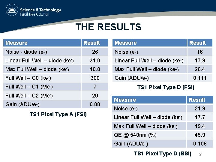
THE RESULTS Measure Result Noise - diode (e-) 26 Measure Result Noise (e-) 18 Linear Full Well – diode (ke-) 31. 0 Linear Full Well – diode (ke-) 17. 9 Max Full Well – diode (ke-) 40. 0 Max Full Well – diode (ke-) 26. 4 Full Well – C 0 (ke-) 300 Gain (ADU/e-) 0. 111 Full Well – C 1 (Me-) 7 Full Well – C 2 (Me-) 20 Gain (ADU/e-) TS 1 Pixel Type A (FSI) 0. 08 TS 1 Pixel Type D (FSI) Measure Result Noise (e-) 21. 9 Linear Full Well – diode (ke-) 17. 7 Max Full Well – diode (ke-) 19. 4 QE @ 540 nm (%) 45. 9 Gain (ADU/e-) 0. 108 TS 1 Pixel Type D (BSI) 21

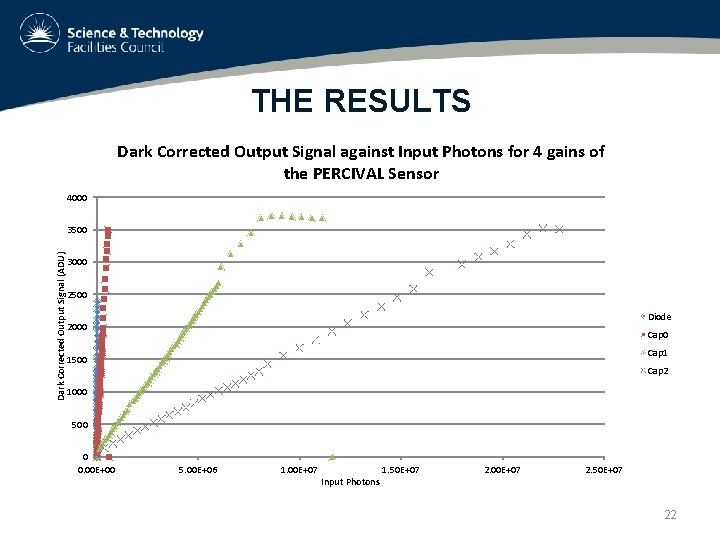
THE RESULTS Dark Corrected Output Signal against Input Photons for 4 gains of the PERCIVAL Sensor 4000 Dark Corrected Output Signal (ADU) 3500 3000 2500 Diode 2000 Cap 1 1500 Cap 2 1000 500 0 0. 00 E+00 5. 00 E+06 1. 00 E+07 Input Photons 1. 50 E+07 2. 00 E+07 2. 50 E+07 22

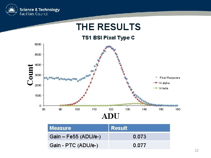
THE RESULTS TS 1 BSI Pixel Type C 6000 Count 5000 4000 3000 Pixel Response K-alpha 2000 K-beta 1000 0 80 90 100 110 120 130 140 150 160 ADU Measure Result Gain – Fe 55 (ADU/e-) 0. 073 Gain - PTC (ADU/e-) 0. 077 23

THE RESULTS 8 -7 MUX 7 BIT SR TS 3 8 COLUMN BLOCK 8 BIT SR 8 BIT SR 8 BIT SR 8 BIT SR 8 BIT SR 8 BIT SR 8 BIT SR 8 BIT SR 4 -1 MUX + LVDS 24

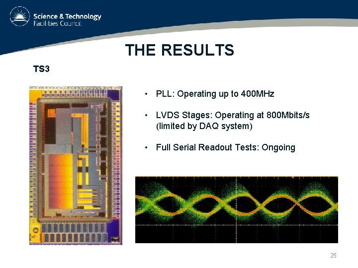
THE RESULTS TS 3 • PLL: Operating up to 400 MHz • LVDS Stages: Operating at 800 Mbits/s (limited by DAQ system) • Full Serial Readout Tests: Ongoing 25

THE FUTURE

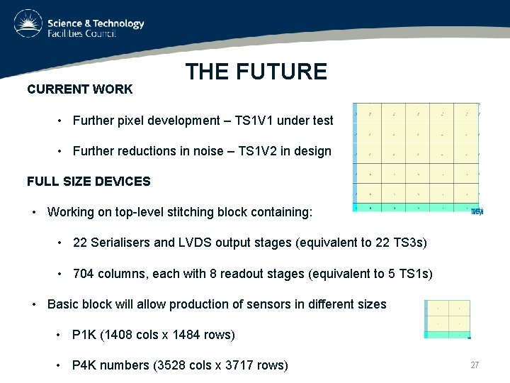
CURRENT WORK THE FUTURE • Further pixel development – TS 1 V 1 under test • Further reductions in noise – TS 1 V 2 in design FULL SIZE DEVICES • Working on top-level stitching block containing: • 22 Serialisers and LVDS output stages (equivalent to 22 TS 3 s) • 704 columns, each with 8 readout stages (equivalent to 5 TS 1 s) • Basic block will allow production of sensors in different sizes • P 1 K (1408 cols x 1484 rows) • P 4 K numbers (3528 cols x 3717 rows) 27

CONCLUSION

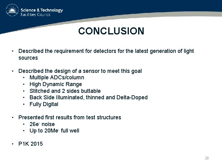
CONCLUSION • Described the requirement for detectors for the latest generation of light sources • Described the design of a sensor to meet this goal • Multiple ADCs/column • High Dynamic Range • Stitched and 2 sides buttable • Back Side Illuminated, thinned and Delta-Doped • Fully Digital • Presented first results from test structures • 26 e- noise • Up to 20 Me- full well • P 1 K 2015 29

Questions? 30