The MGPA ECAL readout chip for CMS MultiGain
![Noise ENC [rms electrons] BARREL END-CAP high gain chan. 7240+5. 8/p. F mid gain Noise ENC [rms electrons] BARREL END-CAP high gain chan. 7240+5. 8/p. F mid gain](https://slidetodoc.com/presentation_image_h/1cd9709e58f748c95b2837ad1fea3bc6/image-12.jpg)
- Slides: 21

The MGPA ECAL readout chip for CMS Multi–Gain Pre-Amplifier - 0. 25 mm CMOS chip for CMS ECAL OUTLINE Introduction & background Design Measured Performance Conclusions Mark Raymond, Geoff Hall, Imperial College London, UK. Jamie Crooks, Marcus French, Rutherford Appleton Laboratory, UK. IEEE Nuclear Science Symposium, Rome 2004 M. Raymond, Imperial College London IEEE NSS, Rome 2004

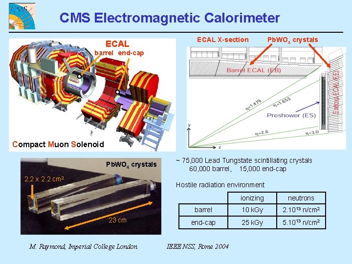
CMS Electromagnetic Calorimeter ECAL X-section Pb. WO 4 crystals barrel end-cap Compact Muon Solenoid Pb. WO 4 crystals 2. 2 x 2. 2 cm 2 ~ 75, 000 Lead Tungstate scintillating crystals 60, 000 barrel, 15, 000 end-cap Hostile radiation environment 23 cm M. Raymond, Imperial College London ionizing neutrons barrel 10 k. Gy 2. 1013 n/cm 2 end-cap 25 k. Gy 5. 1013 n/cm 2 IEEE NSS, Rome 2004

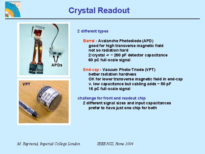
Crystal Readout 2 different types Barrel - Avalanche Photodiode (APD) good for high transverse magnetic field not so radiation hard 2/crystal -> ~ 200 p. F detector capacitance 60 p. C full-scale signal APDs End-cap - Vacuum Photo-Triode (VPT) better radiation hardness OK for lower transverse magnetic field in end-cap v. low capacitance but cabling adds ~ 50 p. F 16 p. C full-scale signal VPT challenge for front end readout chip 2 different signal sizes and input capacitances prefer to have just one chip for both M. Raymond, Imperial College London IEEE NSS, Rome 2004

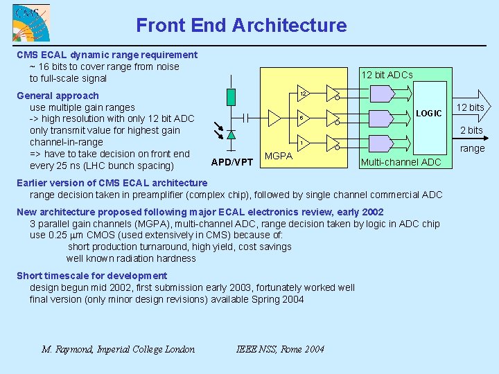
Front End Architecture CMS ECAL dynamic range requirement ~ 16 bits to cover range from noise to full-scale signal General approach use multiple gain ranges -> high resolution with only 12 bit ADC only transmit value for highest gain channel-in-range => have to take decision on front end every 25 ns (LHC bunch spacing) 12 bit ADCs 12 6 LOGIC 2 bits 1 APD/VPT MGPA range Multi-channel ADC Earlier version of CMS ECAL architecture range decision taken in preamplifier (complex chip), followed by single channel commercial ADC New architecture proposed following major ECAL electronics review, early 2002 3 parallel gain channels (MGPA), multi-channel ADC, range decision taken by logic in ADC chip use 0. 25 mm CMOS (used extensively in CMS) because of: short production turnaround, high yield, cost savings well known radiation hardness Short timescale for development design begun mid 2002, first submission early 2003, fortunately worked well final version (only minor design revisions) available Spring 2004 M. Raymond, Imperial College London 12 bits IEEE NSS, Rome 2004

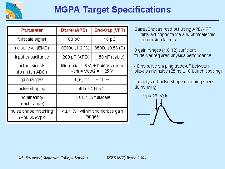
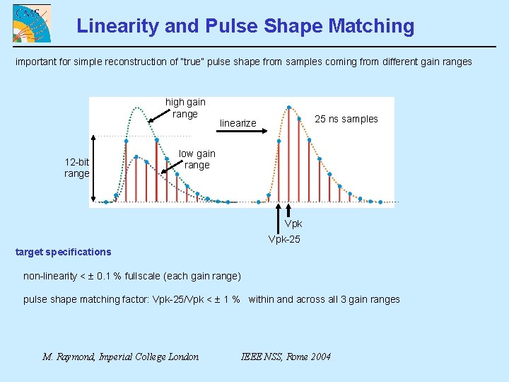
MGPA Target Specifications Parameter Barrel (APD) End-Cap (VPT) fullscale signal 60 p. C 16 p. C noise level (ENC) 10000 e (1. 6 f. C) 3500 e (0. 56 f. C) input capacitance ~ 200 p. F (APD) ~ 50 p. F (cable) output signals (to match ADC) gain ranges differential 1. 8 V, 0. 45 V around Vcm = Vdd/2 = 1. 25 V 1, 6, 12 10 % pulse shaping 40 ns CR-RC nonlinearity (each range) < 0. 1 % fullscale pulse shape matching (Vpk-25)/Vpk < 1 % within and across gain ranges M. Raymond, Imperial College London Barrel/Endcap read out using APD/VPT different capacitance and photoelectric conversion factors 3 gain ranges (1: 6: 12) sufficient to deliver required physics performance 40 ns pulse shaping trade-off between pile-up and noise (25 ns LHC bunch spacing) linearity and pulse shape matching specs demanding Vpk-25 Vpk IEEE NSS, Rome 2004

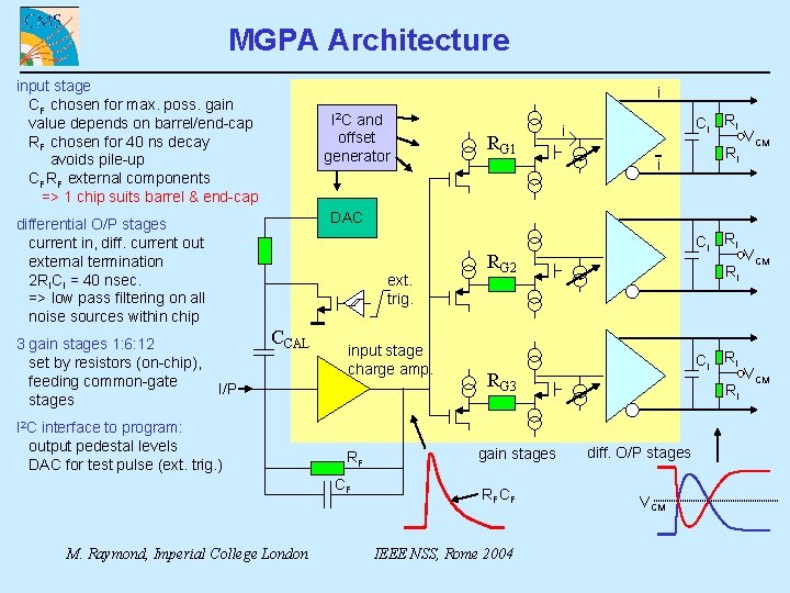
MGPA Architecture input stage CF chosen for max. poss. gain value depends on barrel/end-cap RF chosen for 40 ns decay avoids pile-up CFRF external components => 1 chip suits barrel & end-cap i I 2 C and offset generator i RI VCM DAC differential O/P stages current in, diff. current out external termination 2 RICI = 40 nsec. => low pass filtering on all noise sources within chip 3 gain stages 1: 6: 12 set by resistors (on-chip), feeding common-gate stages RG 1 CI RI i ext. trig. CCAL input stage charge amp. I/P I 2 C interface to program: output pedestal levels DAC for test pulse (ext. trig. ) RF CF M. Raymond, Imperial College London CI RI RG 2 RI CI RI RG 3 gain stages RFCF IEEE NSS, Rome 2004 RI diff. O/P stages VCM VCM

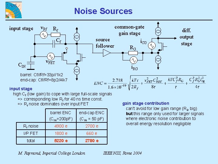
Noise Sources input stage v. Rf common-gate gain stage source i. CG follower RG Rf Cf v. FET CIN diff. output stage i. RG barrel: Cf//Rf=33 p//1 k 2 end-cap: Cf//Rf=8 p 2//4 k 7 input stage high Cf (low gain) to cope with large full-scale signals => corresponding low Rf for 40 ns time const. => Rf noise dominates over input FET barrel ENC (CIN=200 p. F) end-cap ENC (CIN = 50 p. F) Rf noise 4900 e 2700 e I/P FET 1800 e 660 e total 5220 e 2780 e M. Raymond, Imperial College London gain stage contribution can’t avoid for low gain range (RG big) but this range only used for larger signals where electronic noise contribution to overall energy resolution negligible IEEE NSS, Rome 2004

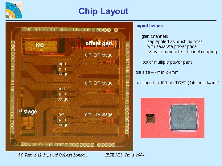
Chip Layout layout issues offset gen. I 2 C diff. O/P stage gain channels segregated as much as poss. with separate power pads -> try to avoid inter-channel coupling lots of multiple power pads high gain stage die size ~ 4 mm x 4 mm diff. O/P stage packaged in 100 pin TQFP (14 mm x 14 mm) mid gain stage 1 st stage low gain stage diff. O/P stage M. Raymond, Imperial College London IEEE NSS, Rome 2004

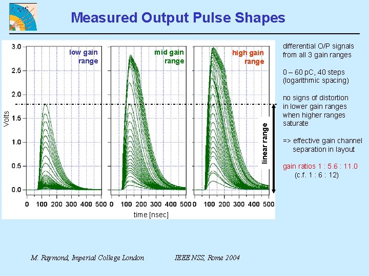
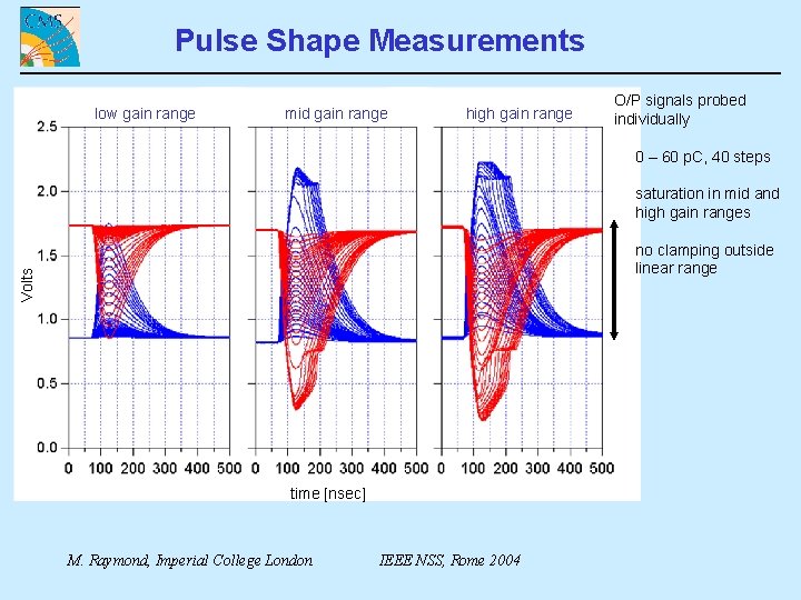
Measured Output Pulse Shapes mid gain range low gain range high gain range differential O/P signals from all 3 gain ranges linear range Volts 0 – 60 p. C, 40 steps (logarithmic spacing) time [nsec] M. Raymond, Imperial College London IEEE NSS, Rome 2004 no signs of distortion in lower gain ranges when higher ranges saturate => effective gain channel separation in layout gain ratios 1 : 5. 6 : 11. 0 (c. f. 1 : 6 : 12)

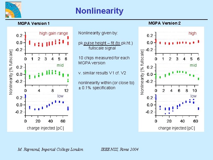
Nonlinearity MGPA Version 2 MGPA Version 1 Nonlinearity given by: pk. pulse height – fit (to pk. ht. ) fullscale signal mid 10 chips measured for each MGPA version v. similar results V 1 cf. V 2 nonlinearity within (or close to) ± 0. 1% specification low charge injected [p. C] M. Raymond, Imperial College London high Nonlinearity [% fullscale] high gain range mid low charge injected [p. C] IEEE NSS, Rome 2004

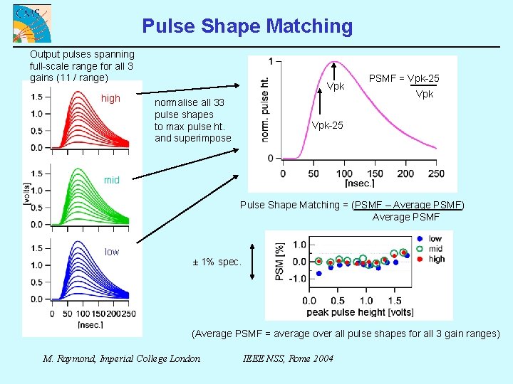
Pulse Shape Matching Output pulses spanning full-scale range for all 3 gains (11 / range) high Vpk normalise all 33 pulse shapes to max pulse ht. and superimpose PSMF = Vpk-25 mid Pulse Shape Matching = (PSMF – Average PSMF) Average PSMF low ± 1% spec. (Average PSMF = average over all pulse shapes for all 3 gain ranges) M. Raymond, Imperial College London IEEE NSS, Rome 2004
![Noise ENC rms electrons BARREL ENDCAP high gain chan 72405 8p F mid gain Noise ENC [rms electrons] BARREL END-CAP high gain chan. 7240+5. 8/p. F mid gain](https://slidetodoc.com/presentation_image_h/1cd9709e58f748c95b2837ad1fea3bc6/image-12.jpg)
Noise ENC [rms electrons] BARREL END-CAP high gain chan. 7240+5. 8/p. F mid gain chan. high gain chan. 7870+4. 9/p. F 3040+4. 5/p. F added capacitance [p. F] 3270+4. 5/p. F added capacitance [p. F] weak dependence on input capacitance as expected within spec. for high and mid-gain ranges: barrel < 10000 e, end-cap < 3500 e low gain range: barrel: 27300 e ± 12% end-cap: 8200 e ± 11% completely dominated by gain stage noise but signals large so < 0. 2% contribution to overall energy resolution M. Raymond, Imperial College London mid gain chan. IEEE NSS, Rome 2004

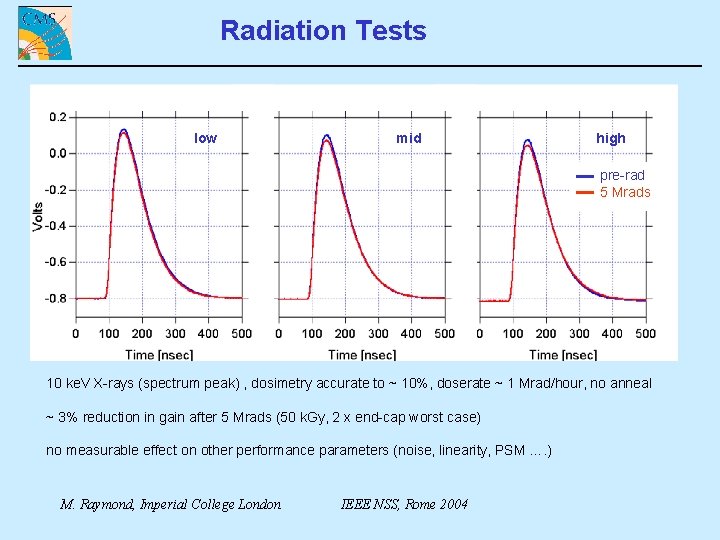
Radiation Tests low mid high pre-rad 5 Mrads 10 ke. V X-rays (spectrum peak) , dosimetry accurate to ~ 10%, doserate ~ 1 Mrad/hour, no anneal ~ 3% reduction in gain after 5 Mrads (50 k. Gy, 2 x end-cap worst case) no measurable effect on other performance parameters (noise, linearity, PSM …. ) M. Raymond, Imperial College London IEEE NSS, Rome 2004

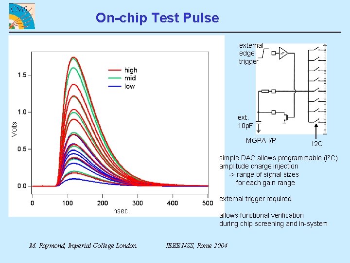
On-chip Test Pulse external edge trigger Volts ext. 10 p. F MGPA I/P I 2 C simple DAC allows programmable (I 2 C) amplitude charge injection -> range of signal sizes for each gain range external trigger required nsec. M. Raymond, Imperial College London allows functional verification during chip screening and in-system IEEE NSS, Rome 2004

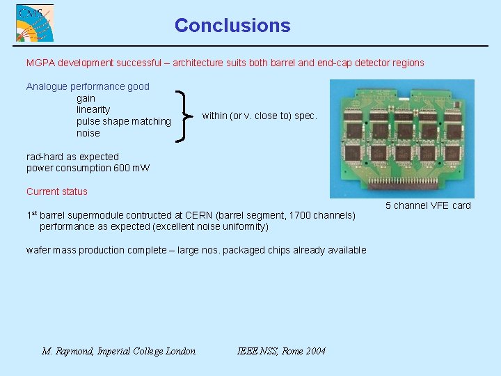
Conclusions MGPA development successful – architecture suits both barrel and end-cap detector regions Analogue performance good gain linearity pulse shape matching noise within (or v. close to) spec. rad-hard as expected power consumption 600 m. W Current status 1 st barrel supermodule contructed at CERN (barrel segment, 1700 channels) performance as expected (excellent noise uniformity) wafer mass production complete – large nos. packaged chips already available M. Raymond, Imperial College London IEEE NSS, Rome 2004 5 channel VFE card

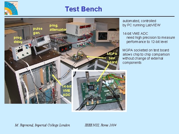
Test Bench pulse gen. automated, controlled by PC running Lab. VIEW prog. attenuator 14 -bit VME ADC need high precision to measure performance to 12 -bit level prog. delay MGPA test board 14 -bit VME ADC M. Raymond, Imperial College London IEEE NSS, Rome 2004 MGPA socketed on test board allows chip to chip comparison without change of external components

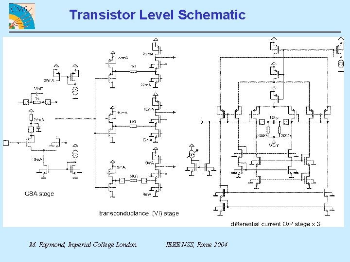
Transistor Level Schematic M. Raymond, Imperial College London IEEE NSS, Rome 2004

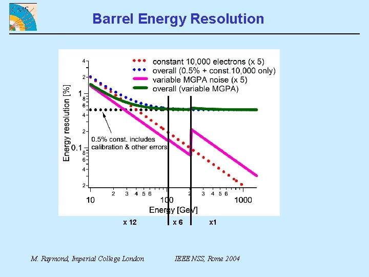
Barrel Energy Resolution x 12 M. Raymond, Imperial College London x 6 x 1 IEEE NSS, Rome 2004

Pulse Shape Measurements low gain range mid gain range high gain range O/P signals probed individually 0 – 60 p. C, 40 steps saturation in mid and high gain ranges Volts no clamping outside linear range time [nsec] M. Raymond, Imperial College London IEEE NSS, Rome 2004

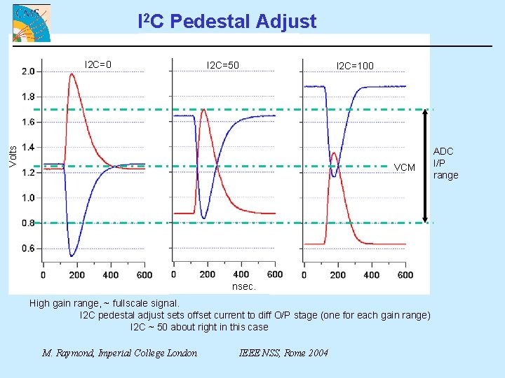
I 2 C Pedestal Adjust I 2 C=50 Volts I 2 C=0 I 2 C=100 VCM nsec. High gain range, ~ fullscale signal. I 2 C pedestal adjust sets offset current to diff O/P stage (one for each gain range) I 2 C ~ 50 about right in this case M. Raymond, Imperial College London IEEE NSS, Rome 2004 ADC I/P range

Linearity and Pulse Shape Matching important for simple reconstruction of “true” pulse shape from samples coming from different gain ranges high gain range 12 -bit range 25 ns samples linearize low gain range Vpk-25 target specifications non-linearity < 0. 1 % fullscale (each gain range) pulse shape matching factor: Vpk-25/Vpk < 1 % within and across all 3 gain ranges M. Raymond, Imperial College London IEEE NSS, Rome 2004