The Memory Hierarchy Cache Main Memory and Virtual



- Slides: 36

The Memory Hierarchy Cache, Main Memory, and Virtual Memory (Part 2) Lecture for CPSC 5155 Edward Bosworth, Ph. D. Computer Science Department Columbus State University

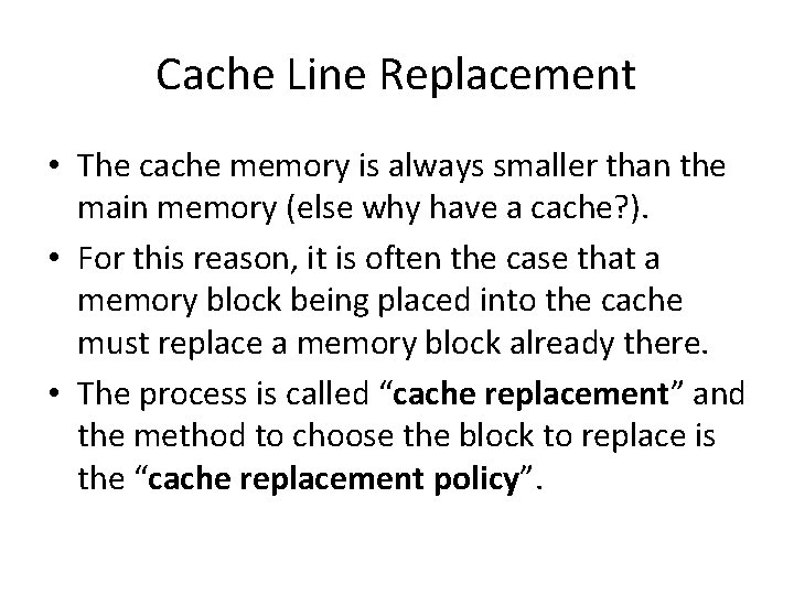
Cache Line Replacement • The cache memory is always smaller than the main memory (else why have a cache? ). • For this reason, it is often the case that a memory block being placed into the cache must replace a memory block already there. • The process is called “cache replacement” and the method to choose the block to replace is the “cache replacement policy”.

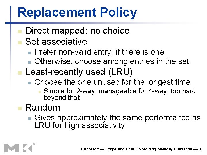
Replacement Policy n n Direct mapped: no choice Set associative n n n Prefer non-valid entry, if there is one Otherwise, choose among entries in the set Least-recently used (LRU) n Choose the one unused for the longest time n n Simple for 2 -way, manageable for 4 -way, too hard beyond that Random n Gives approximately the same performance as LRU for high associativity Chapter 5 — Large and Fast: Exploiting Memory Hierarchy — 3

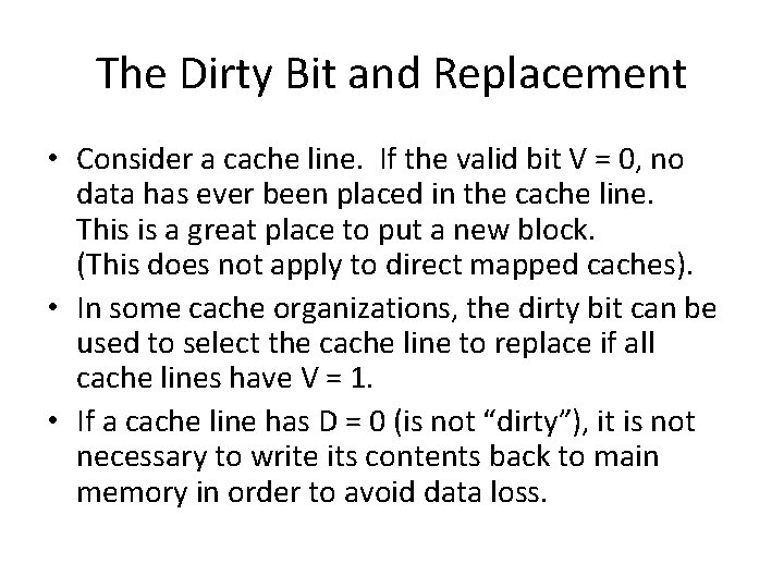
The Dirty Bit and Replacement • Consider a cache line. If the valid bit V = 0, no data has ever been placed in the cache line. This is a great place to put a new block. (This does not apply to direct mapped caches). • In some cache organizations, the dirty bit can be used to select the cache line to replace if all cache lines have V = 1. • If a cache line has D = 0 (is not “dirty”), it is not necessary to write its contents back to main memory in order to avoid data loss.

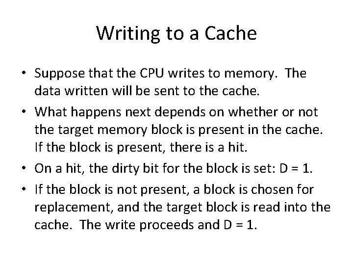
Writing to a Cache • Suppose that the CPU writes to memory. The data written will be sent to the cache. • What happens next depends on whether or not the target memory block is present in the cache. If the block is present, there is a hit. • On a hit, the dirty bit for the block is set: D = 1. • If the block is not present, a block is chosen for replacement, and the target block is read into the cache. The write proceeds and D = 1.

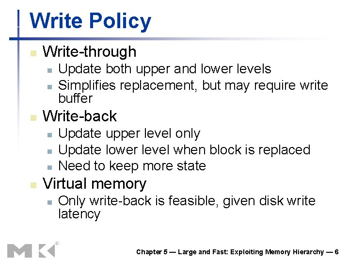
Write Policy n Write-through n n n Write-back n n Update both upper and lower levels Simplifies replacement, but may require write buffer Update upper level only Update lower level when block is replaced Need to keep more state Virtual memory n Only write-back is feasible, given disk write latency Chapter 5 — Large and Fast: Exploiting Memory Hierarchy — 6

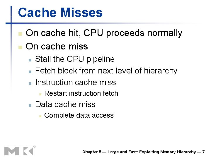
Cache Misses n n On cache hit, CPU proceeds normally On cache miss n n n Stall the CPU pipeline Fetch block from next level of hierarchy Instruction cache miss n n Restart instruction fetch Data cache miss n Complete data access Chapter 5 — Large and Fast: Exploiting Memory Hierarchy — 7

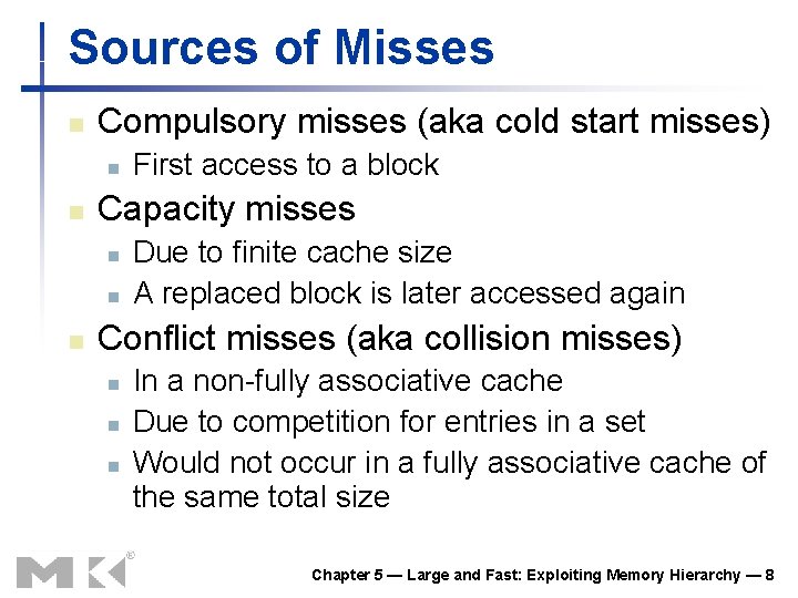
Sources of Misses n Compulsory misses (aka cold start misses) n n Capacity misses n n n First access to a block Due to finite cache size A replaced block is later accessed again Conflict misses (aka collision misses) n n n In a non-fully associative cache Due to competition for entries in a set Would not occur in a fully associative cache of the same total size Chapter 5 — Large and Fast: Exploiting Memory Hierarchy — 8

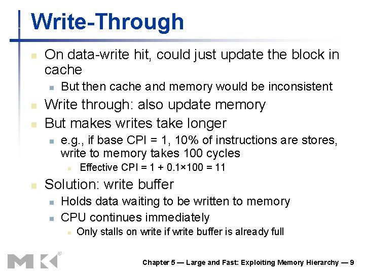
Write-Through n On data-write hit, could just update the block in cache n n n But then cache and memory would be inconsistent Write through: also update memory But makes writes take longer n e. g. , if base CPI = 1, 10% of instructions are stores, write to memory takes 100 cycles n n Effective CPI = 1 + 0. 1× 100 = 11 Solution: write buffer n n Holds data waiting to be written to memory CPU continues immediately n Only stalls on write if write buffer is already full Chapter 5 — Large and Fast: Exploiting Memory Hierarchy — 9

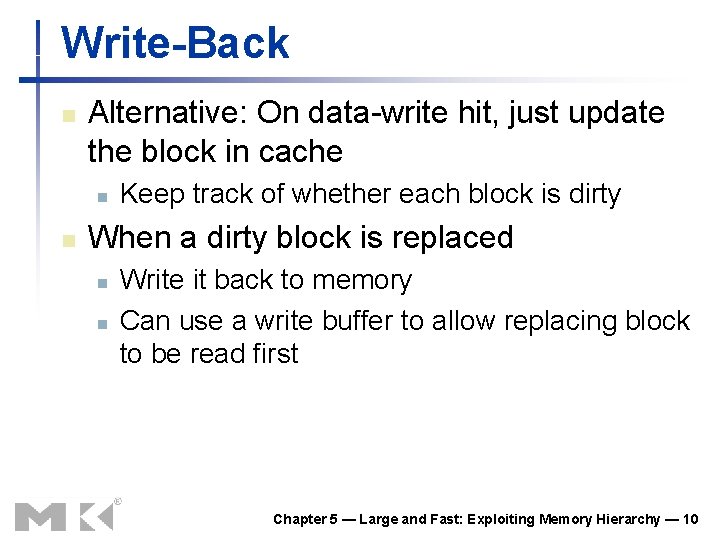
Write-Back n Alternative: On data-write hit, just update the block in cache n n Keep track of whether each block is dirty When a dirty block is replaced n n Write it back to memory Can use a write buffer to allow replacing block to be read first Chapter 5 — Large and Fast: Exploiting Memory Hierarchy — 10

Write Allocation n n What should happen on a write miss? Alternatives for write-through n n Allocate on miss: fetch the block Write around: don’t fetch the block n n Since programs often write a whole block before reading it (e. g. , initialization) For write-back n Usually fetch the block Chapter 5 — Large and Fast: Exploiting Memory Hierarchy — 11

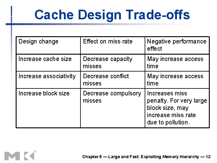
Cache Design Trade-offs Design change Effect on miss rate Negative performance effect Increase cache size Decrease capacity misses May increase access time Increase associativity Decrease conflict misses May increase access time Increase block size Decrease compulsory misses Increases miss penalty. For very large block size, may increase miss rate due to pollution. Chapter 5 — Large and Fast: Exploiting Memory Hierarchy — 12

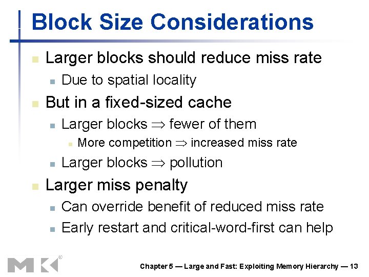
Block Size Considerations n Larger blocks should reduce miss rate n n Due to spatial locality But in a fixed-sized cache n Larger blocks fewer of them n n n More competition increased miss rate Larger blocks pollution Larger miss penalty n n Can override benefit of reduced miss rate Early restart and critical-word-first can help Chapter 5 — Large and Fast: Exploiting Memory Hierarchy — 13

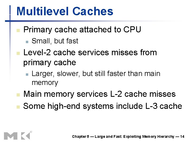
Multilevel Caches n Primary cache attached to CPU n n Level-2 cache services misses from primary cache n n n Small, but fast Larger, slower, but still faster than main memory Main memory services L-2 cache misses Some high-end systems include L-3 cache Chapter 5 — Large and Fast: Exploiting Memory Hierarchy — 14

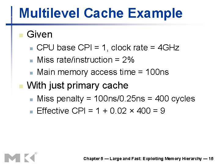
Multilevel Cache Example n Given n n CPU base CPI = 1, clock rate = 4 GHz Miss rate/instruction = 2% Main memory access time = 100 ns With just primary cache n n Miss penalty = 100 ns/0. 25 ns = 400 cycles Effective CPI = 1 + 0. 02 × 400 = 9 Chapter 5 — Large and Fast: Exploiting Memory Hierarchy — 15

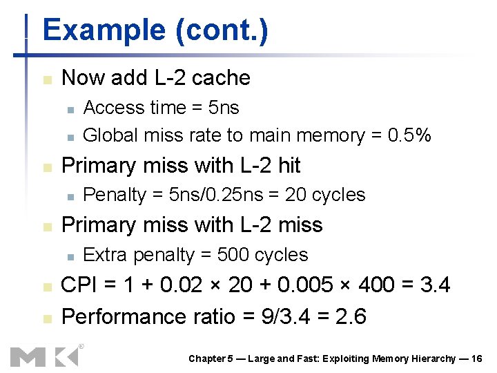
Example (cont. ) n Now add L-2 cache n n n Primary miss with L-2 hit n n n Penalty = 5 ns/0. 25 ns = 20 cycles Primary miss with L-2 miss n n Access time = 5 ns Global miss rate to main memory = 0. 5% Extra penalty = 500 cycles CPI = 1 + 0. 02 × 20 + 0. 005 × 400 = 3. 4 Performance ratio = 9/3. 4 = 2. 6 Chapter 5 — Large and Fast: Exploiting Memory Hierarchy — 16

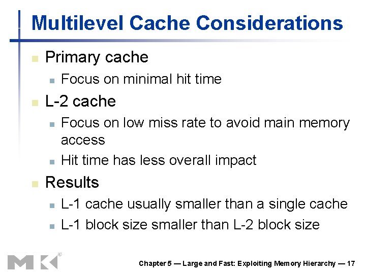
Multilevel Cache Considerations n Primary cache n n L-2 cache n n n Focus on minimal hit time Focus on low miss rate to avoid main memory access Hit time has less overall impact Results n n L-1 cache usually smaller than a single cache L-1 block size smaller than L-2 block size Chapter 5 — Large and Fast: Exploiting Memory Hierarchy — 17

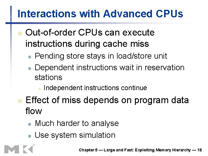
Interactions with Advanced CPUs n Out-of-order CPUs can execute instructions during cache miss n n Pending store stays in load/store unit Dependent instructions wait in reservation stations n n Independent instructions continue Effect of miss depends on program data flow n n Much harder to analyse Use system simulation Chapter 5 — Large and Fast: Exploiting Memory Hierarchy — 18

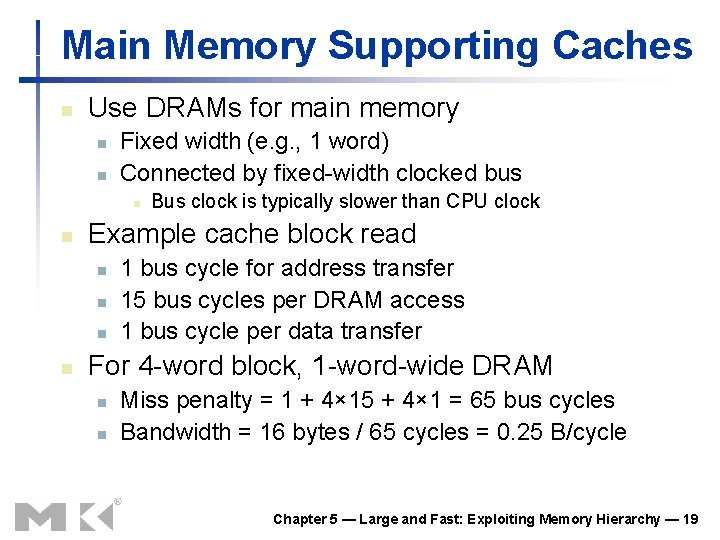
Main Memory Supporting Caches n Use DRAMs for main memory n n Fixed width (e. g. , 1 word) Connected by fixed-width clocked bus n n Example cache block read n n Bus clock is typically slower than CPU clock 1 bus cycle for address transfer 15 bus cycles per DRAM access 1 bus cycle per data transfer For 4 -word block, 1 -word-wide DRAM n n Miss penalty = 1 + 4× 15 + 4× 1 = 65 bus cycles Bandwidth = 16 bytes / 65 cycles = 0. 25 B/cycle Chapter 5 — Large and Fast: Exploiting Memory Hierarchy — 19

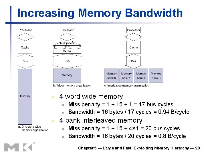
Increasing Memory Bandwidth n 4 -word wide memory n n n Miss penalty = 1 + 15 + 1 = 17 bus cycles Bandwidth = 16 bytes / 17 cycles = 0. 94 B/cycle 4 -bank interleaved memory n n Miss penalty = 1 + 15 + 4× 1 = 20 bus cycles Bandwidth = 16 bytes / 20 cycles = 0. 8 B/cycle Chapter 5 — Large and Fast: Exploiting Memory Hierarchy — 20

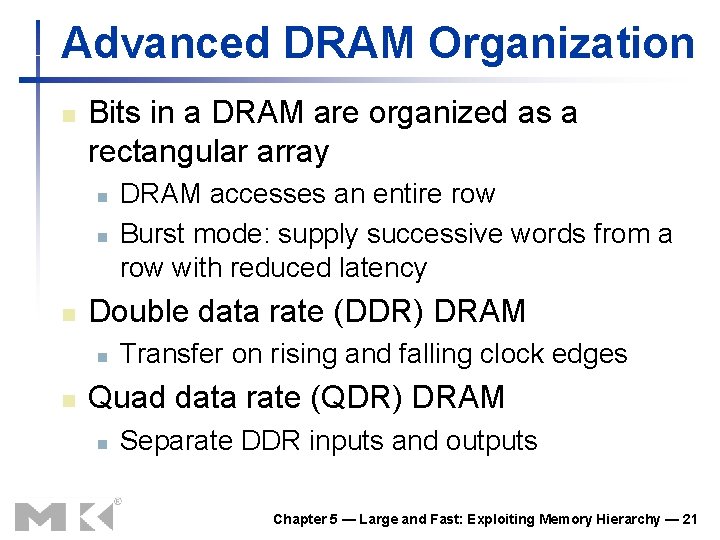
Advanced DRAM Organization n Bits in a DRAM are organized as a rectangular array n n n Double data rate (DDR) DRAM n n DRAM accesses an entire row Burst mode: supply successive words from a row with reduced latency Transfer on rising and falling clock edges Quad data rate (QDR) DRAM n Separate DDR inputs and outputs Chapter 5 — Large and Fast: Exploiting Memory Hierarchy — 21

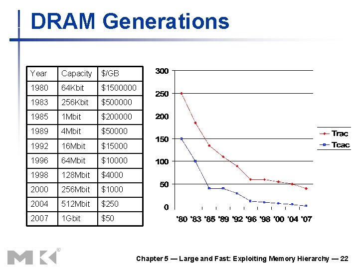
DRAM Generations Year Capacity $/GB 1980 64 Kbit $1500000 1983 256 Kbit $500000 1985 1 Mbit $200000 1989 4 Mbit $50000 1992 16 Mbit $15000 1996 64 Mbit $10000 1998 128 Mbit $4000 256 Mbit $1000 2004 512 Mbit $250 2007 1 Gbit $50 Chapter 5 — Large and Fast: Exploiting Memory Hierarchy — 22

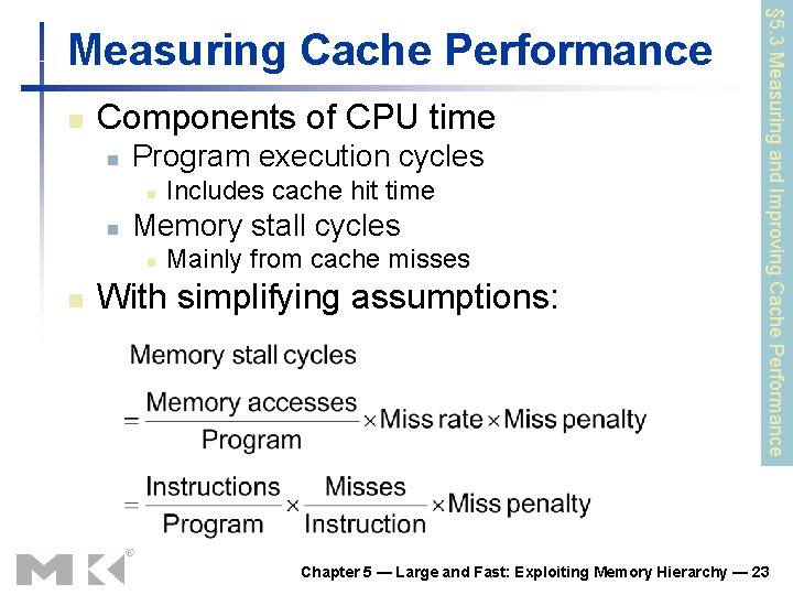
n Components of CPU time n Program execution cycles n n Memory stall cycles n n Includes cache hit time Mainly from cache misses With simplifying assumptions: § 5. 3 Measuring and Improving Cache Performance Measuring Cache Performance Chapter 5 — Large and Fast: Exploiting Memory Hierarchy — 23

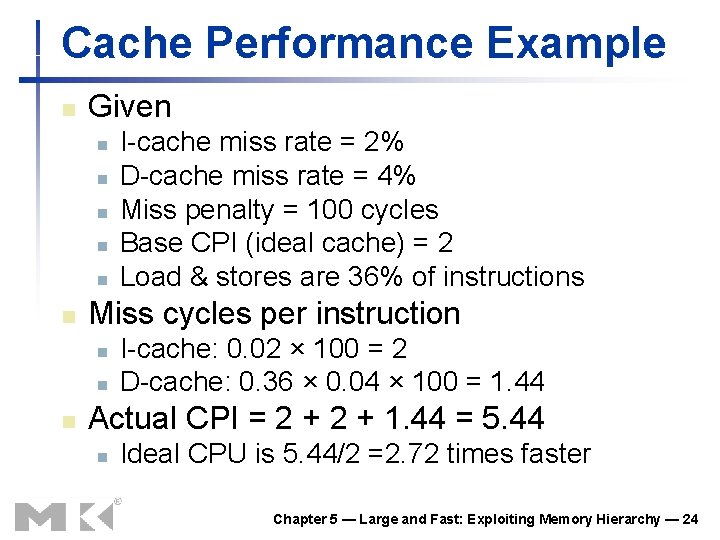
Cache Performance Example n Given n n n Miss cycles per instruction n I-cache miss rate = 2% D-cache miss rate = 4% Miss penalty = 100 cycles Base CPI (ideal cache) = 2 Load & stores are 36% of instructions I-cache: 0. 02 × 100 = 2 D-cache: 0. 36 × 0. 04 × 100 = 1. 44 Actual CPI = 2 + 1. 44 = 5. 44 n Ideal CPU is 5. 44/2 =2. 72 times faster Chapter 5 — Large and Fast: Exploiting Memory Hierarchy — 24

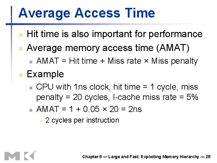
Average Access Time n n Hit time is also important for performance Average memory access time (AMAT) n n AMAT = Hit time + Miss rate × Miss penalty Example n n CPU with 1 ns clock, hit time = 1 cycle, miss penalty = 20 cycles, I-cache miss rate = 5% AMAT = 1 + 0. 05 × 20 = 2 ns n 2 cycles per instruction Chapter 5 — Large and Fast: Exploiting Memory Hierarchy — 25

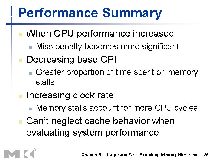
Performance Summary n When CPU performance increased n n Decreasing base CPI n n Greater proportion of time spent on memory stalls Increasing clock rate n n Miss penalty becomes more significant Memory stalls account for more CPU cycles Can’t neglect cache behavior when evaluating system performance Chapter 5 — Large and Fast: Exploiting Memory Hierarchy — 26

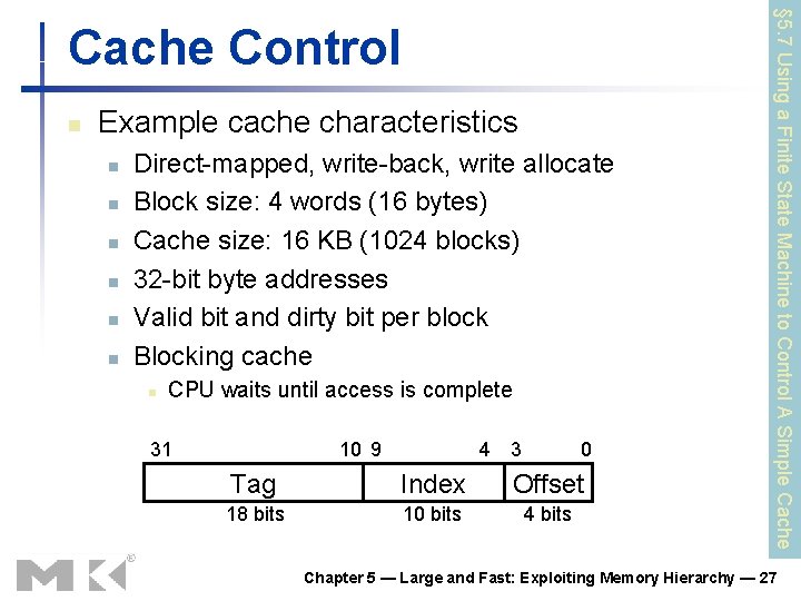
n Example cache characteristics n n n Direct-mapped, write-back, write allocate Block size: 4 words (16 bytes) Cache size: 16 KB (1024 blocks) 32 -bit byte addresses Valid bit and dirty bit per block Blocking cache n CPU waits until access is complete 31 10 9 4 3 0 Tag Index Offset 18 bits 10 bits 4 bits § 5. 7 Using a Finite State Machine to Control A Simple Cache Control Chapter 5 — Large and Fast: Exploiting Memory Hierarchy — 27

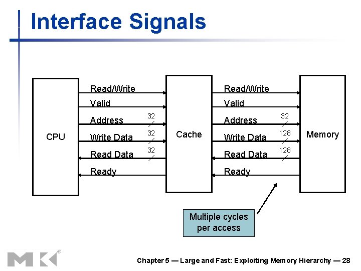
Interface Signals CPU Read/Write Valid Address 32 Write Data 32 Ready Cache Address 32 Write Data 128 Read Data 128 Memory Ready Multiple cycles per access Chapter 5 — Large and Fast: Exploiting Memory Hierarchy — 28

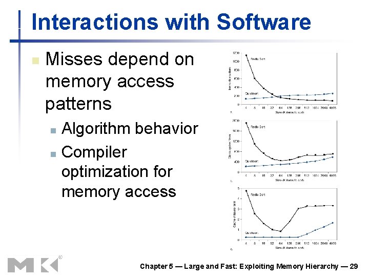
Interactions with Software n Misses depend on memory access patterns Algorithm behavior n Compiler optimization for memory access n Chapter 5 — Large and Fast: Exploiting Memory Hierarchy — 29

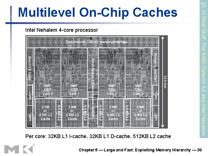
Intel Nehalem 4 -core processor Per core: 32 KB L 1 I-cache, 32 KB L 1 D-cache, 512 KB L 2 cache § 5. 10 Real Stuff: The AMD Opteron X 4 and Intel Nehalem Multilevel On-Chip Caches Chapter 5 — Large and Fast: Exploiting Memory Hierarchy — 30

3 -Level Cache Organization Intel Nehalem AMD Opteron X 4 L 1 caches (per core) L 1 I-cache: 32 KB, 64 -byte blocks, 4 -way, approx LRU replacement, hit time n/a L 1 D-cache: 32 KB, 64 -byte blocks, 8 -way, approx LRU replacement, writeback/allocate, hit time n/a L 1 I-cache: 32 KB, 64 -byte blocks, 2 -way, LRU replacement, hit time 3 cycles L 1 D-cache: 32 KB, 64 -byte blocks, 2 -way, LRU replacement, writeback/allocate, hit time 9 cycles L 2 unified cache (per core) 256 KB, 64 -byte blocks, 8 -way, 512 KB, 64 -byte blocks, 16 -way, approx LRU replacement, write- approx LRU replacement, writeback/allocate, hit time n/a L 3 unified cache (shared) 8 MB, 64 -byte blocks, 16 -way, replacement n/a, writeback/allocate, hit time n/a 2 MB, 64 -byte blocks, 32 -way, replace block shared by fewest cores, write-back/allocate, hit time 32 cycles n/a: data not available Chapter 5 — Large and Fast: Exploiting Memory Hierarchy — 31

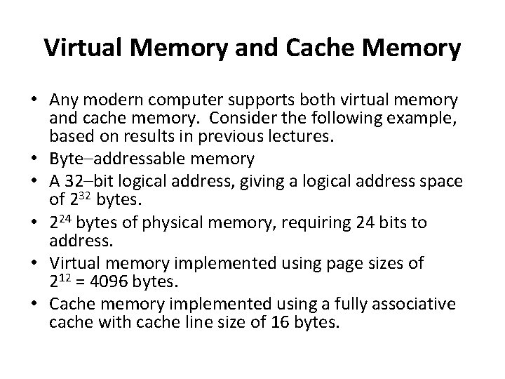
Virtual Memory and Cache Memory • Any modern computer supports both virtual memory and cache memory. Consider the following example, based on results in previous lectures. • Byte–addressable memory • A 32–bit logical address, giving a logical address space of 232 bytes. • 224 bytes of physical memory, requiring 24 bits to address. • Virtual memory implemented using page sizes of 212 = 4096 bytes. • Cache memory implemented using a fully associative cache with cache line size of 16 bytes.

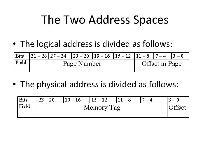
The Two Address Spaces • The logical address is divided as follows: Bits 31 – 28 27 – 24 23 – 20 19 – 16 Field Page Number 15 – 12 11 – 8 7– 4 3– 0 Offset in Page • The physical address is divided as follows: Bits Field 23 – 20 19 – 16 15 – 12 11 – 8 Memory Tag 7– 4 3– 0 Offset

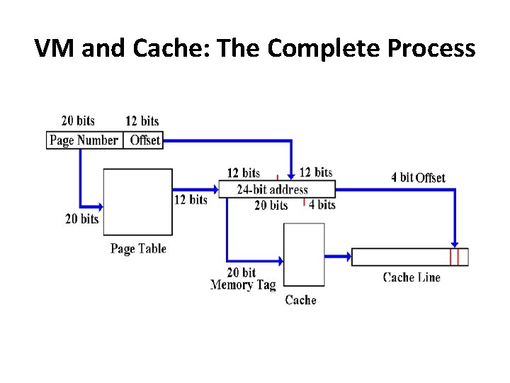
VM and Cache: The Complete Process

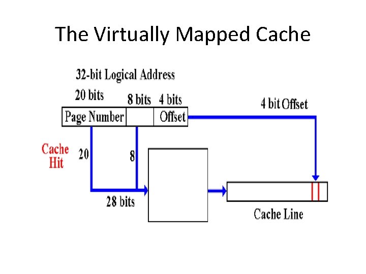
The Virtually Mapped Cache

Problems with Virtually Mapped Caches • Cache misses have to invoke the virtual memory system (more on that later). This is not a problem. • One problem with virtual mapping is that the translation from virtual addresses to physical addresses varies between processes. This is called the “aliasing problem”. • A solution is to extend the virtual address by a process id.