The IEEE 1149 4 std for mixedsignal test
![Experiment #2 (observe A 0 at AT 2): SVF code ABM[A 0]: SD + Experiment #2 (observe A 0 at AT 2): SVF code ABM[A 0]: SD +](https://slidetodoc.com/presentation_image_h2/d85483f56be0a862cf639bd4304bd02c/image-56.jpg)
![Experiment #3: Measuring R [A 0 -GND] (SVF code) ABM[A 0]: SB 1 + Experiment #3: Measuring R [A 0 -GND] (SVF code) ABM[A 0]: SB 1 +](https://slidetodoc.com/presentation_image_h2/d85483f56be0a862cf639bd4304bd02c/image-59.jpg)
- Slides: 60

The IEEE 1149. 4 std for mixedsignal test J. M. Martins Ferreira FEUP / DEEC - Rua Dr. Roberto Frias 4200 -537 Porto - PORTUGAL Tel. 351 225 081 748 / Fax: 351 225 081 443 (jmf@fe. up. pt / http: //www. fe. up. pt/~jmf) Introduction to design for test techniques – The IEEE 1149. 4 std for mixed-signal test © J. M. Martins Ferreira - University of Porto (FEUP / DEEC) 1

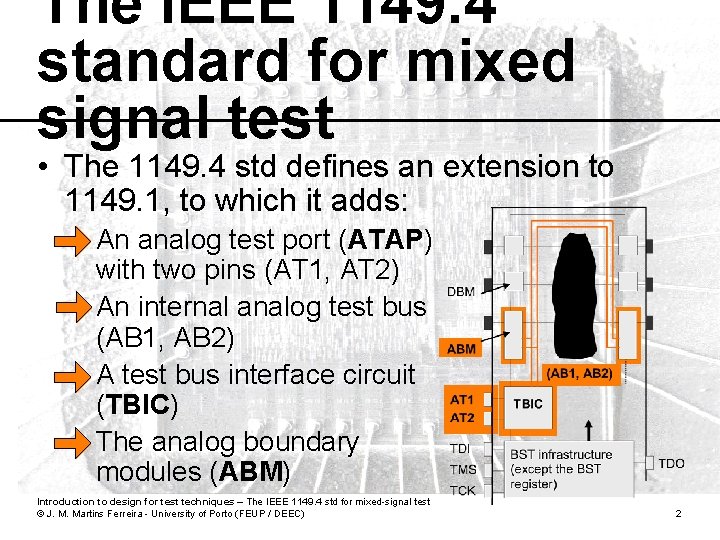
The IEEE 1149. 4 standard for mixed signal test • The 1149. 4 std defines an extension to 1149. 1, to which it adds: – An analog test port (ATAP) with two pins (AT 1, AT 2) – An internal analog test bus (AB 1, AB 2) – A test bus interface circuit (TBIC) – The analog boundary modules (ABM) Introduction to design for test techniques – The IEEE 1149. 4 std for mixed-signal test © J. M. Martins Ferreira - University of Porto (FEUP / DEEC) 2

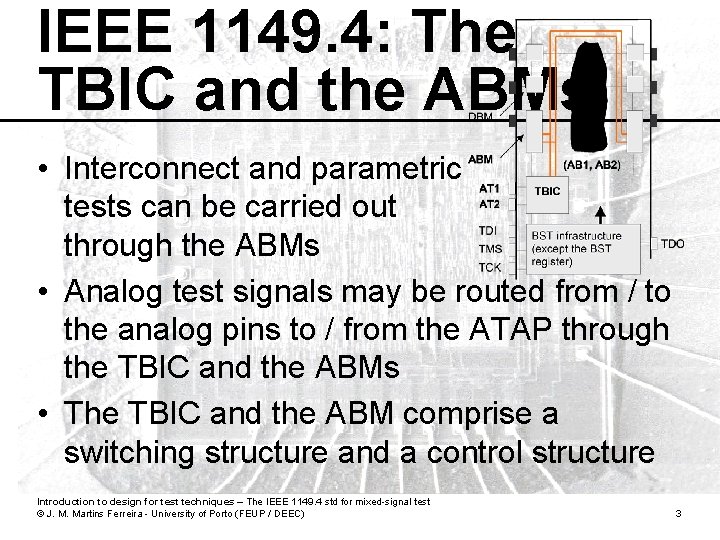
IEEE 1149. 4: The TBIC and the ABMs • Interconnect and parametric tests can be carried out through the ABMs • Analog test signals may be routed from / to the analog pins to / from the ATAP through the TBIC and the ABMs • The TBIC and the ABM comprise a switching structure and a control structure Introduction to design for test techniques – The IEEE 1149. 4 std for mixed-signal test © J. M. Martins Ferreira - University of Porto (FEUP / DEEC) 3

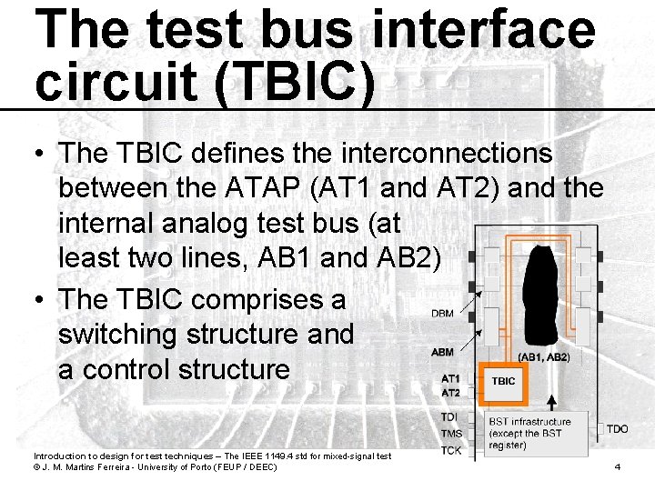
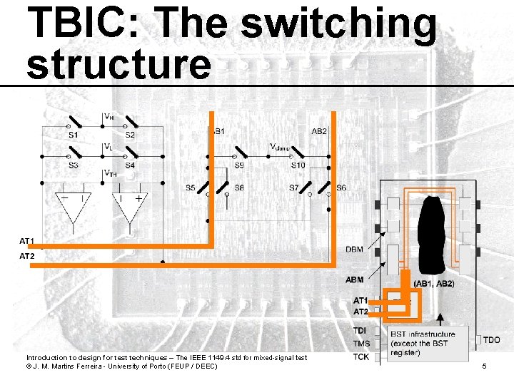
The test bus interface circuit (TBIC) • The TBIC defines the interconnections between the ATAP (AT 1 and AT 2) and the internal analog test bus (at least two lines, AB 1 and AB 2) • The TBIC comprises a switching structure and a control structure Introduction to design for test techniques – The IEEE 1149. 4 std for mixed-signal test © J. M. Martins Ferreira - University of Porto (FEUP / DEEC) 4

TBIC: The switching structure Introduction to design for test techniques – The IEEE 1149. 4 std for mixed-signal test © J. M. Martins Ferreira - University of Porto (FEUP / DEEC) 5

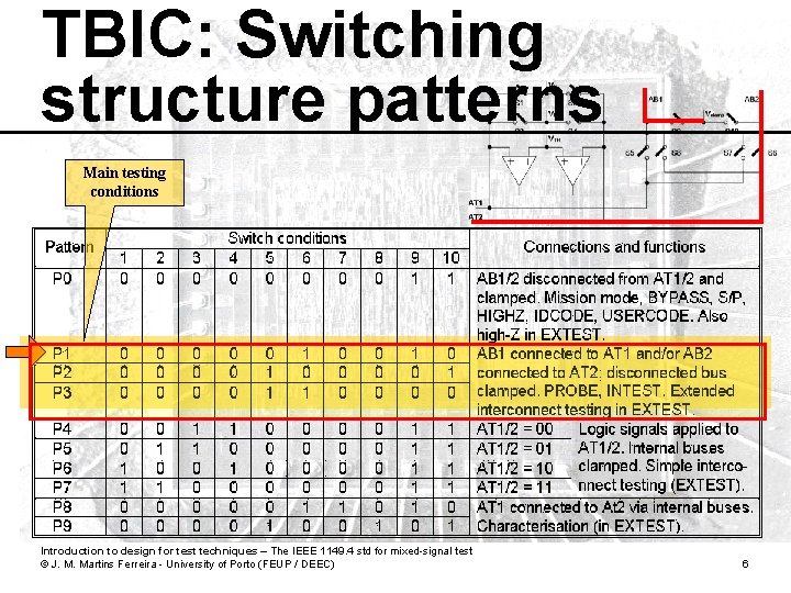
TBIC: Switching structure patterns Main testing conditions Introduction to design for test techniques – The IEEE 1149. 4 std for mixed-signal test © J. M. Martins Ferreira - University of Porto (FEUP / DEEC) 6

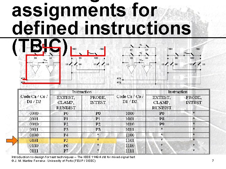
assignments for defined instructions (TBIC) Introduction to design for test techniques – The IEEE 1149. 4 std for mixed-signal test © J. M. Martins Ferreira - University of Porto (FEUP / DEEC) 7

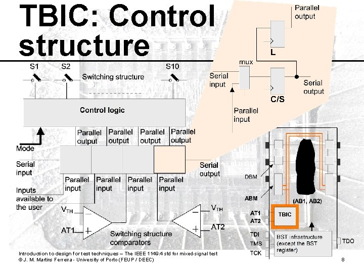
TBIC: Control structure Introduction to design for test techniques – The IEEE 1149. 4 std for mixed-signal test © J. M. Martins Ferreira - University of Porto (FEUP / DEEC) 8

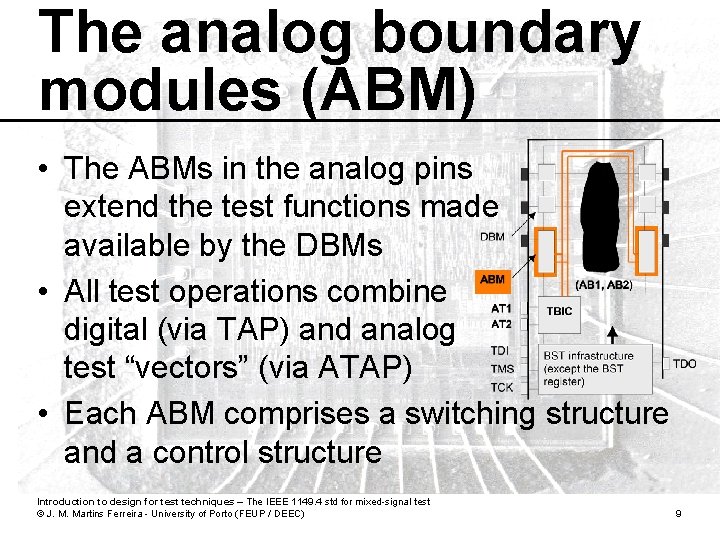
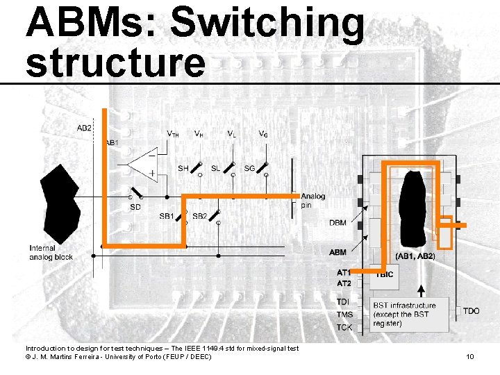
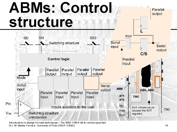
The analog boundary modules (ABM) • The ABMs in the analog pins extend the test functions made available by the DBMs • All test operations combine digital (via TAP) and analog test “vectors” (via ATAP) • Each ABM comprises a switching structure and a control structure Introduction to design for test techniques – The IEEE 1149. 4 std for mixed-signal test © J. M. Martins Ferreira - University of Porto (FEUP / DEEC) 9

ABMs: Switching structure Introduction to design for test techniques – The IEEE 1149. 4 std for mixed-signal test © J. M. Martins Ferreira - University of Porto (FEUP / DEEC) 10

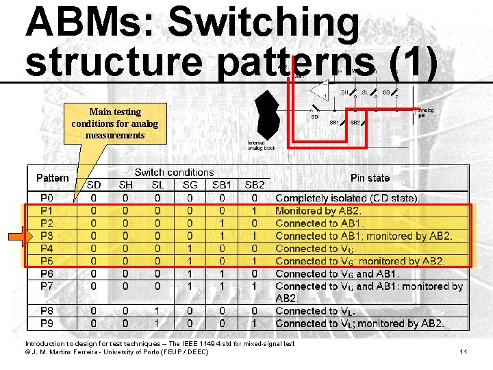
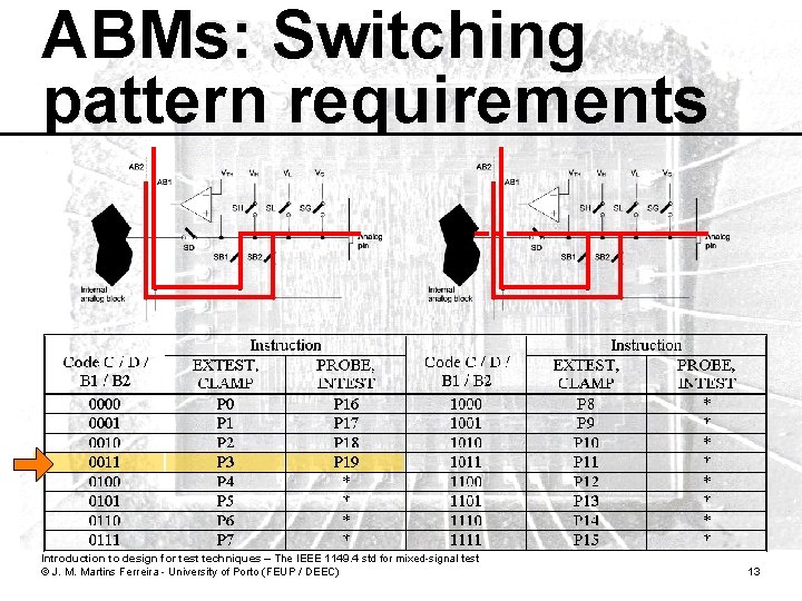
ABMs: Switching structure patterns (1) Main testing conditions for analog measurements Introduction to design for test techniques – The IEEE 1149. 4 std for mixed-signal test © J. M. Martins Ferreira - University of Porto (FEUP / DEEC) 11

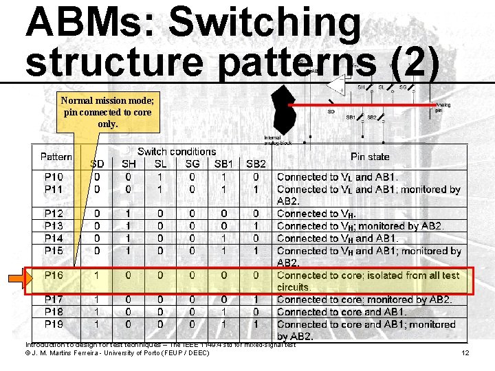
ABMs: Switching structure patterns (2) Normal mission mode; pin connected to core only. Introduction to design for test techniques – The IEEE 1149. 4 std for mixed-signal test © J. M. Martins Ferreira - University of Porto (FEUP / DEEC) 12

ABMs: Switching pattern requirements Introduction to design for test techniques – The IEEE 1149. 4 std for mixed-signal test © J. M. Martins Ferreira - University of Porto (FEUP / DEEC) 13

ABMs: Control structure Introduction to design for test techniques – The IEEE 1149. 4 std for mixed-signal test © J. M. Martins Ferreira - University of Porto (FEUP / DEEC) 14

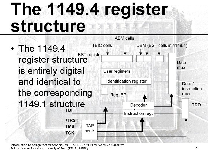
The 1149. 4 register structure • The 1149. 4 register structure is entirely digital and identical to the corresponding 1149. 1 structure Introduction to design for test techniques – The IEEE 1149. 4 std for mixed-signal test © J. M. Martins Ferreira - University of Porto (FEUP / DEEC) 15

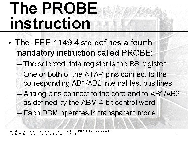
The PROBE instruction • The IEEE 1149. 4 std defines a fourth mandatory instruction called PROBE: – The selected data register is the BS register – One or both of the ATAP pins connect to the corresponding AB 1/AB 2 internal test bus lines – Analog pins connect to the core and to AB 1/AB 2 as defined by the ABM 4 -bit control word – Each DBM operates in transparent mode Introduction to design for test techniques – The IEEE 1149. 4 std for mixed-signal test © J. M. Martins Ferreira - University of Porto (FEUP / DEEC) 16

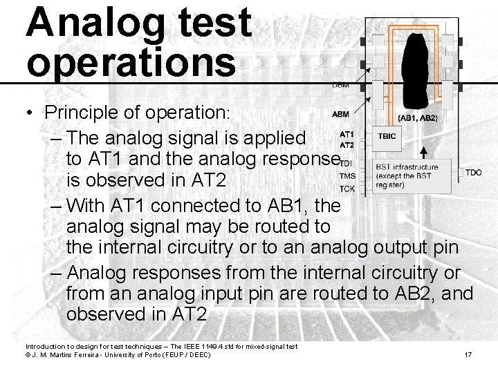
Analog test operations • Principle of operation: – The analog signal is applied to AT 1 and the analog response is observed in AT 2 – With AT 1 connected to AB 1, the analog signal may be routed to the internal circuitry or to an analog output pin – Analog responses from the internal circuitry or from an analog input pin are routed to AB 2, and observed in AT 2 Introduction to design for test techniques – The IEEE 1149. 4 std for mixed-signal test © J. M. Martins Ferreira - University of Porto (FEUP / DEEC) 17

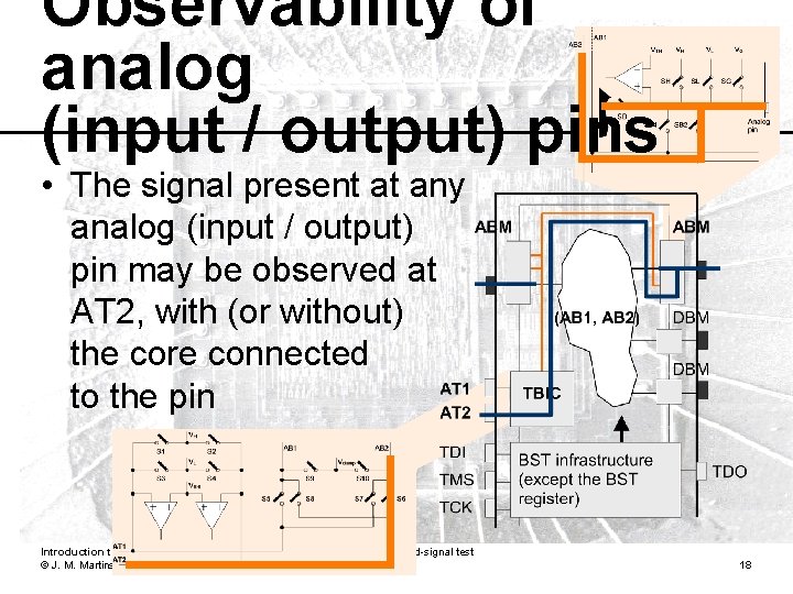
Observability of analog (input / output) pins • The signal present at any analog (input / output) pin may be observed at AT 2, with (or without) the core connected to the pin Introduction to design for test techniques – The IEEE 1149. 4 std for mixed-signal test © J. M. Martins Ferreira - University of Porto (FEUP / DEEC) 18

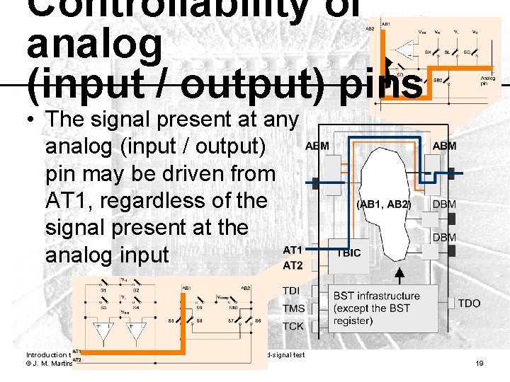
Controllability of analog (input / output) pins • The signal present at any analog (input / output) pin may be driven from AT 1, regardless of the signal present at the analog input Introduction to design for test techniques – The IEEE 1149. 4 std for mixed-signal test © J. M. Martins Ferreira - University of Porto (FEUP / DEEC) 19

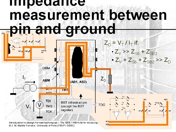
Impedance measurement between pin and ground ZD = VT / IT if: • ZV >> ZS 6 + ZSB 2 • ZV + ZS 6 + ZSB 2 >> ZD IT ZD VT V Introduction to design for test techniques – The IEEE 1149. 4 std for mixed-signal test © J. M. Martins Ferreira - University of Porto (FEUP / DEEC) 20

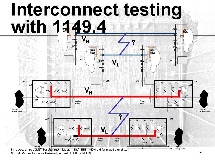
Interconnect testing with 1149. 4 VH ? VL Introduction to design for test techniques – The IEEE 1149. 4 std for mixed-signal test © J. M. Martins Ferreira - University of Porto (FEUP / DEEC) 21

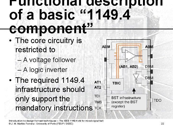
Functional description of a basic “ 1149. 4 component” • The core circuitry is restricted to – A voltage follower – A logic inverter • The required 1149. 4 infrastructure should only support the mandatory instructions Introduction to design for test techniques – The IEEE 1149. 4 std for mixed-signal test © J. M. Martins Ferreira - University of Porto (FEUP / DEEC) 22

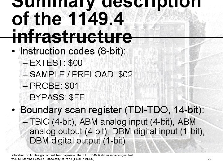
Summary description of the 1149. 4 infrastructure • Instruction codes (8 -bit): – EXTEST: $00 – SAMPLE / PRELOAD: $02 – PROBE: $01 – BYPASS: $FF • Boundary scan register (TDI-TDO, 14 -bit): – TBIC (4 -bit), ABM analog input (4 -bit), ABM analog output (4 -bit), DBM digital input (1 -bit), DBM digital output (1 -bit) Introduction to design for test techniques – The IEEE 1149. 4 std for mixed-signal test © J. M. Martins Ferreira - University of Porto (FEUP / DEEC) 23

Implementation details • The digital test infrastructure and core logic was implemented by Dr. Gustavo Alves in an EPM 7128 Altera PLD (2, 500 usable gates, 128 macrocells, 84 pin PLCC) • All remaining blocks are implemented using discrete components (ADG 452 + MAX 4512 analog switches, LM 311 comparators, TL 081 Op. Amp) Introduction to design for test techniques – The IEEE 1149. 4 std for mixed-signal test © J. M. Martins Ferreira - University of Porto (FEUP / DEEC) 24

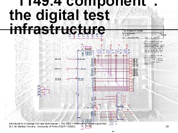
“ 1149. 4 component”: the digital test infrastructure Introduction to design for test techniques – The IEEE 1149. 4 std for mixed-signal test © J. M. Martins Ferreira - University of Porto (FEUP / DEEC) 25

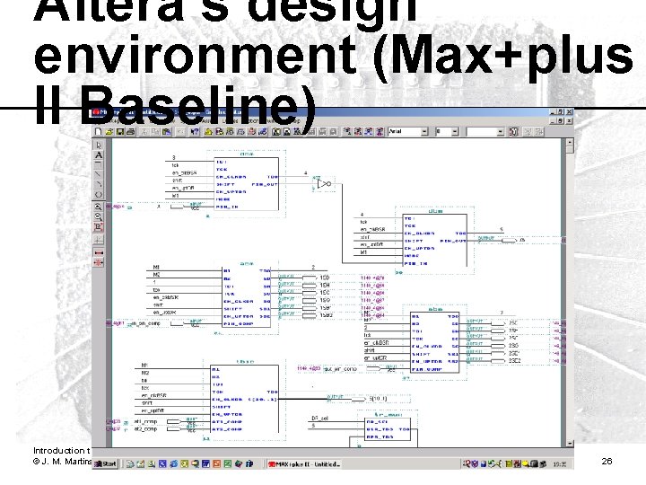
Altera’s design environment (Max+plus II Baseline) Introduction to design for test techniques – The IEEE 1149. 4 std for mixed-signal test © J. M. Martins Ferreira - University of Porto (FEUP / DEEC) 26

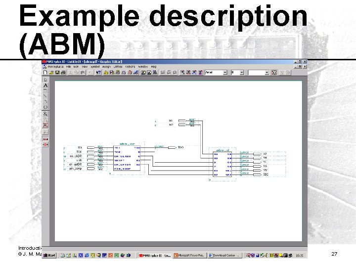
Example description (ABM) Introduction to design for test techniques – The IEEE 1149. 4 std for mixed-signal test © J. M. Martins Ferreira - University of Porto (FEUP / DEEC) 27

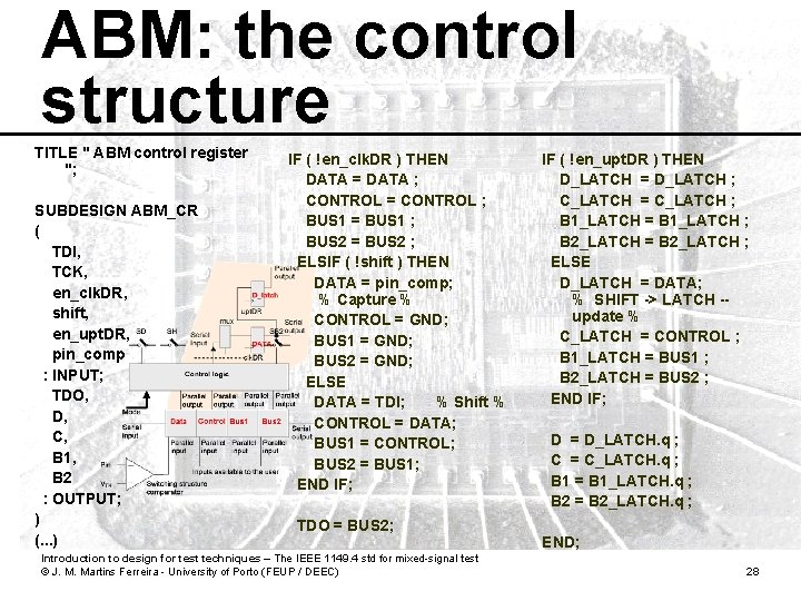
ABM: the control structure TITLE " ABM control register "; SUBDESIGN ABM_CR ( TDI, TCK, en_clk. DR, shift, en_upt. DR, pin_comp : INPUT; TDO, D, C, B 1, B 2 : OUTPUT; ) (. . . ) IF ( !en_clk. DR ) THEN DATA = DATA ; CONTROL = CONTROL ; BUS 1 = BUS 1 ; BUS 2 = BUS 2 ; ELSIF ( !shift ) THEN DATA = pin_comp; % Capture % CONTROL = GND; BUS 1 = GND; BUS 2 = GND; ELSE DATA = TDI; % Shift % CONTROL = DATA; BUS 1 = CONTROL; BUS 2 = BUS 1; END IF; TDO = BUS 2; Introduction to design for test techniques – The IEEE 1149. 4 std for mixed-signal test © J. M. Martins Ferreira - University of Porto (FEUP / DEEC) IF ( !en_upt. DR ) THEN D_LATCH = D_LATCH ; C_LATCH = C_LATCH ; B 1_LATCH = B 1_LATCH ; B 2_LATCH = B 2_LATCH ; ELSE D_LATCH = DATA; % SHIFT -> LATCH -update % C_LATCH = CONTROL ; B 1_LATCH = BUS 1 ; B 2_LATCH = BUS 2 ; END IF; D = D_LATCH. q ; C = C_LATCH. q ; B 1 = B 1_LATCH. q ; B 2 = B 2_LATCH. q ; END; 28

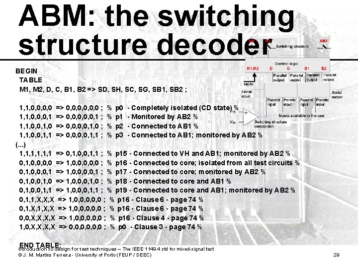
ABM: the switching structure decoder BEGIN TABLE M 1, M 2, D, C, B 1, B 2 => SD, SH, SC, SG, SB 1, SB 2 ; 1, 1, 0, 0 => 0, 0, 0, 0 ; % p 0 - Completely isolated (CD state) % 1, 1, 0, 0, 0, 1 => 0, 0, 0, 1 ; % p 1 - Monitored by AB 2 % 1, 1, 0, 0, 1, 0 => 0, 0, 1, 0 ; % p 2 - Connected to AB 1 % 1, 1, 0, 0, 1, 1 => 0, 0, 1, 1 ; % p 3 - Connected to AB 1; monitored by AB 2 % (. . . ) 1, 1, 1, 1 => 0, 1, 0, 0, 1, 1 ; % p 15 - Connected to VH and AB 1; monitored by AB 2 % 0, 1, 0, 0 => 1, 0, 0, 0 ; % p 16 - Connected to core; isolated from all test circuits % 0, 1, 0, 0, 0, 1 => 1, 0, 0, 1 ; % p 17 - Connected to core; monitored by AB 2 % 0, 1, 0, 0, 1, 0 => 1, 0, 0, 0, 1, 0 ; % p 18 - Connected to core and AB 1 % 0, 1, 0, 0, 1, 1 => 1, 0, 0, 0, 1, 1 ; % p 19 - Connected to core and AB 1; monitored by AB 2 % 0, 1, 1, X, X, X => 1, 0, 0, 0 ; % p 16 - Clause 6 - page 74 % 0, 1, X, X => 1, 0, 0, 0 ; % p 16 - Clause 6 - page 74 % 0, 0, X, X => 1, 0, 0, 0 ; % p 16 - Clause 4 - page 74 % 1, 0, X, X => 0, 0, 0, 0 ; % p 0 - Clause 3 - page 74 % END TABLE; Introduction to design for test techniques – The IEEE 1149. 4 std for mixed-signal test © J. M. Martins Ferreira - University of Porto (FEUP / DEEC) 29

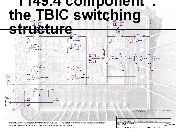
“ 1149. 4 component”: the TBIC switching structure Introduction to design for test techniques – The IEEE 1149. 4 std for mixed-signal test © J. M. Martins Ferreira - University of Porto (FEUP / DEEC) 30

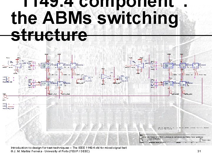
“ 1149. 4 component”: the ABMs switching structure Introduction to design for test techniques – The IEEE 1149. 4 std for mixed-signal test © J. M. Martins Ferreira - University of Porto (FEUP / DEEC) 31

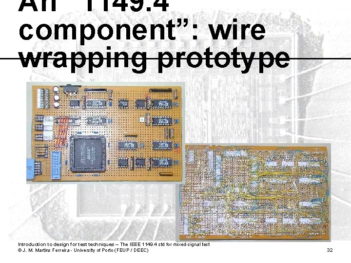
An “ 1149. 4 component”: wire wrapping prototype Introduction to design for test techniques – The IEEE 1149. 4 std for mixed-signal test © J. M. Martins Ferreira - University of Porto (FEUP / DEEC) 32

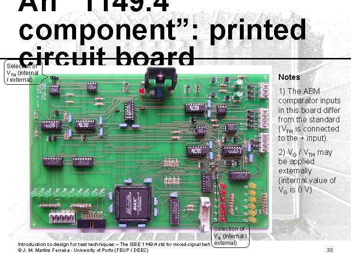
An “ 1149. 4 component”: printed circuit board Selection of VTH (internal / external) Notes: 1) The ABM comparator inputs in this board differ from the standard (VTH is connected to the + input). 2) VG / VTH may be applied externally (internal value of VG is 0 V) Selection of VG (internal / Introduction to design for test techniques – The IEEE 1149. 4 std for mixed-signal test external) © J. M. Martins Ferreira - University of Porto (FEUP / DEEC) 33

Proposed experiments: observability + controllability • Two experiments will be demonstrated using the wire-wrapping “ 1149. 4 component”: – The waveform at the analog output pin will be observed at AT 2, when the analog input is driven by a sine wave – The waveform at the analog output pin will be driven from AT 1 (a square wave), instead of the sine wave coming from the internal circuitry Introduction to design for test techniques – The IEEE 1149. 4 std for mixed-signal test © J. M. Martins Ferreira - University of Porto (FEUP / DEEC) 34

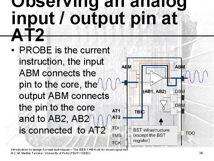
Observing an analog input / output pin at AT 2 • PROBE is the current instruction, the input ABM connects the pin to the core, the output ABM connects the pin to the core and to AB 2, AB 2 is connected to AT 2 Introduction to design for test techniques – The IEEE 1149. 4 std for mixed-signal test © J. M. Martins Ferreira - University of Porto (FEUP / DEEC) 35

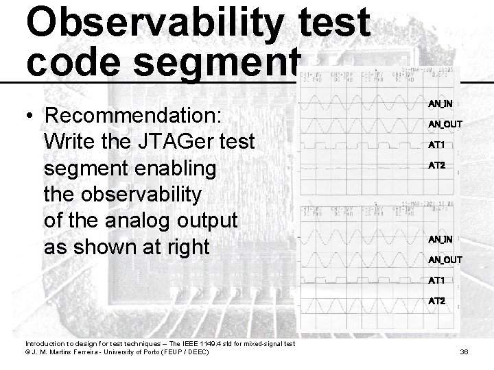
Observability test code segment • Recommendation: Write the JTAGer test segment enabling the observability of the analog output as shown at right AN_IN AN_OUT AT 1 AT 2 Introduction to design for test techniques – The IEEE 1149. 4 std for mixed-signal test © J. M. Martins Ferreira - University of Porto (FEUP / DEEC) 36

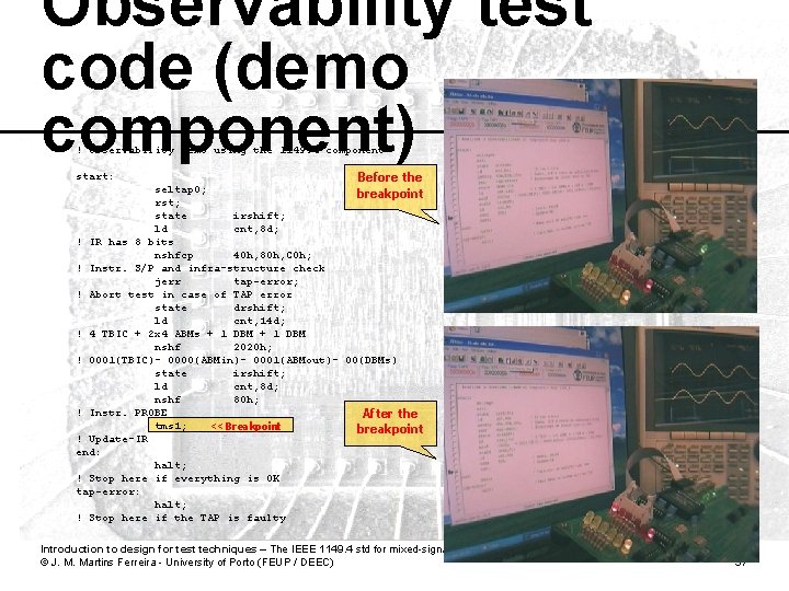
Observability test code (demo component) ! Observability demo using the 1149. 4 component start: Before the seltap 0; breakpoint rst; state irshift; ld cnt, 8 d; ! IR has 8 bits nshfcp 40 h, 80 h, C 0 h; ! Instr. S/P and infra-structure check jerr tap-error; ! Abort test in case of TAP error state drshift; ld cnt, 14 d; ! 4 TBIC + 2 x 4 ABMs + 1 DBM nshf 2020 h; ! 0001(TBIC)- 0000(ABMin)- 0001(ABMout)- 00(DBMs) state irshift; ld cnt, 8 d; nshf 80 h; ! Instr. PROBE After the tms 1; << Breakpoint breakpoint ! Update-IR end: halt; ! Stop here if everything is OK tap-error: halt; ! Stop here if the TAP is faulty Introduction to design for test techniques – The IEEE 1149. 4 std for mixed-signal test © J. M. Martins Ferreira - University of Porto (FEUP / DEEC) 37

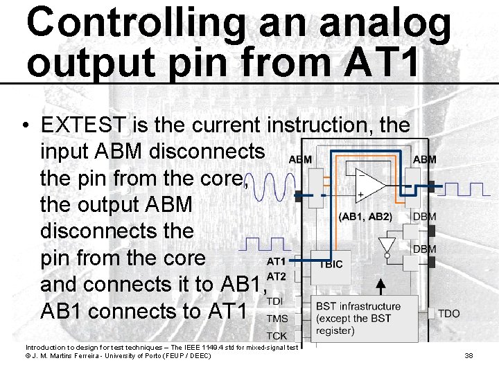
Controlling an analog output pin from AT 1 • EXTEST is the current instruction, the input ABM disconnects the pin from the core, the output ABM disconnects the pin from the core and connects it to AB 1, AB 1 connects to AT 1 Introduction to design for test techniques – The IEEE 1149. 4 std for mixed-signal test © J. M. Martins Ferreira - University of Porto (FEUP / DEEC) 38

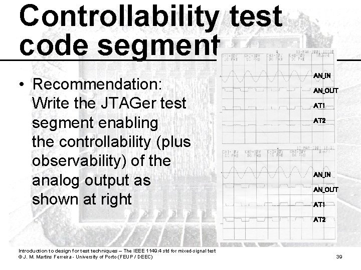
Controllability test code segment • Recommendation: Write the JTAGer test segment enabling the controllability (plus observability) of the analog output as shown at right AN_IN AN_OUT AT 1 AT 2 Introduction to design for test techniques – The IEEE 1149. 4 std for mixed-signal test © J. M. Martins Ferreira - University of Porto (FEUP / DEEC) 39

Video-demos: Observability and controllability Introduction to design for test techniques – The IEEE 1149. 4 std for mixed-signal test © J. M. Martins Ferreira - University of Porto (FEUP / DEEC) (the wmv and bst files are stored in the hibu 2 k 4misc folder) 40

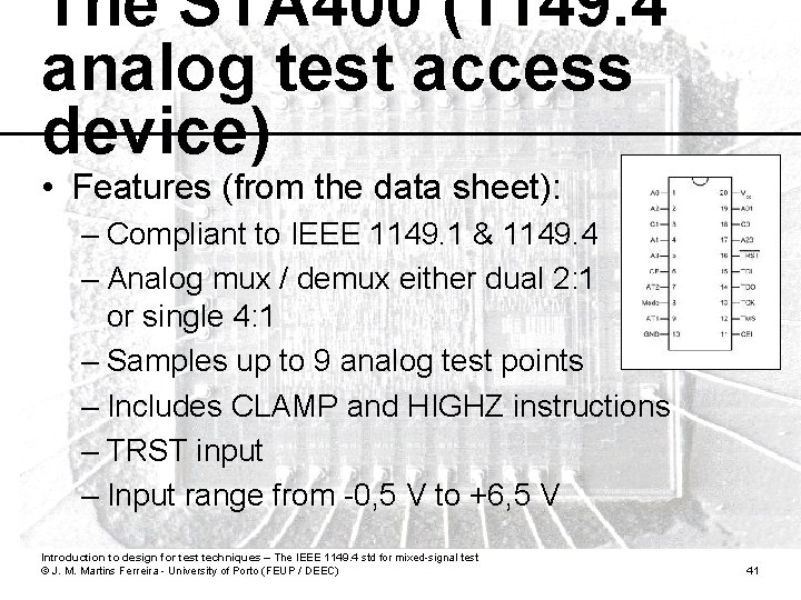
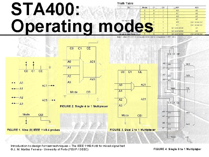
The STA 400 (1149. 4 analog test access device) • Features (from the data sheet): – Compliant to IEEE 1149. 1 & 1149. 4 – Analog mux / demux either dual 2: 1 or single 4: 1 – Samples up to 9 analog test points – Includes CLAMP and HIGHZ instructions – TRST input – Input range from -0, 5 V to +6, 5 V Introduction to design for test techniques – The IEEE 1149. 4 std for mixed-signal test © J. M. Martins Ferreira - University of Porto (FEUP / DEEC) 41

STA 400: Operating modes Introduction to design for test techniques – The IEEE 1149. 4 std for mixed-signal test © J. M. Martins Ferreira - University of Porto (FEUP / DEEC) 42

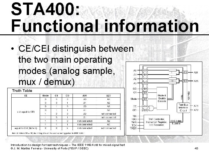
STA 400: Functional information • CE/CEI distinguish between the two main operating modes (analog sample, mux / demux) Introduction to design for test techniques – The IEEE 1149. 4 std for mixed-signal test © J. M. Martins Ferreira - University of Porto (FEUP / DEEC) 43

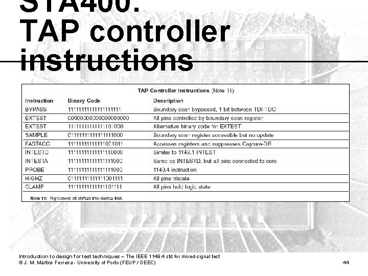
STA 400: TAP controller instructions Introduction to design for test techniques – The IEEE 1149. 4 std for mixed-signal test © J. M. Martins Ferreira - University of Porto (FEUP / DEEC) 44

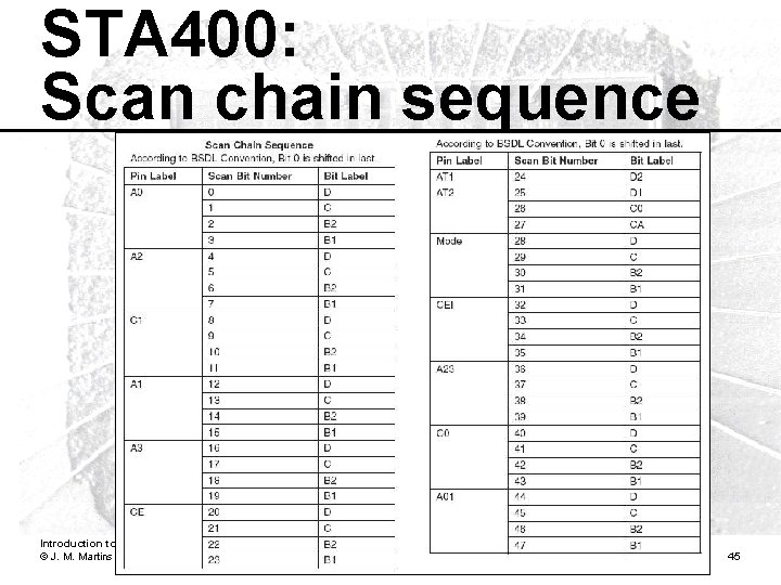
STA 400: Scan chain sequence Introduction to design for test techniques – The IEEE 1149. 4 std for mixed-signal test © J. M. Martins Ferreira - University of Porto (FEUP / DEEC) 45

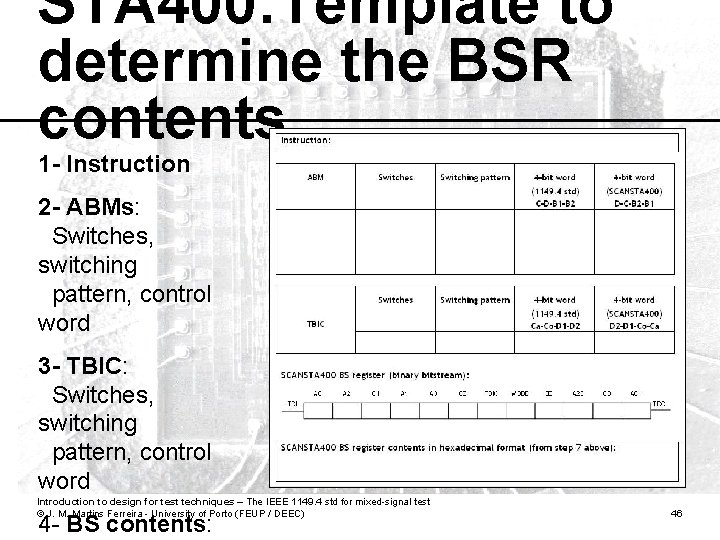
STA 400: Template to determine the BSR contents 1 - Instruction 2 - ABMs: Switches, switching pattern, control word 3 - TBIC: Switches, switching pattern, control word Introduction to design for test techniques – The IEEE 1149. 4 std for mixed-signal test © J. M. Martins Ferreira - University of Porto (FEUP / DEEC) 4 - BS contents: 46

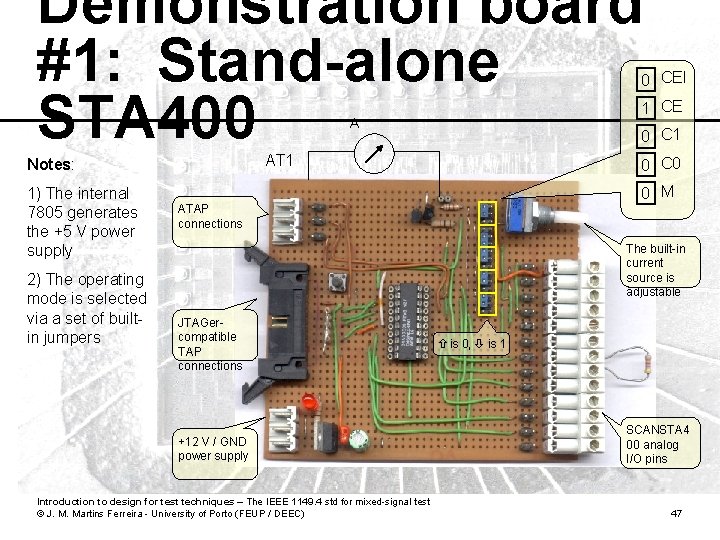
Demonstration board #1: Stand-alone STA 400 0 CEI 1 CE A AT 1 Notes: 1) The internal 7805 generates the +5 V power supply 2) The operating mode is selected via a set of builtin jumpers 0 C 1 0 C 0 0 M ATAP connections The built-in current source is adjustable JTAGercompatible TAP connections +12 V / GND power supply Introduction to design for test techniques – The IEEE 1149. 4 std for mixed-signal test © J. M. Martins Ferreira - University of Porto (FEUP / DEEC) is 0, is 1 SCANSTA 4 00 analog I/O pins 47

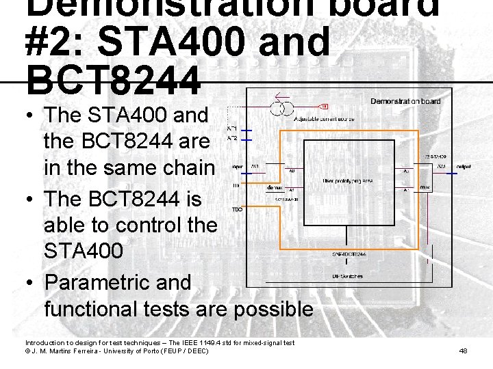
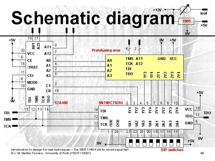
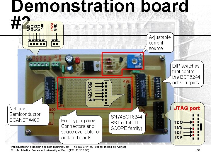
Demonstration board #2: STA 400 and BCT 8244 • The STA 400 and the BCT 8244 are in the same chain • The BCT 8244 is able to control the STA 400 • Parametric and functional tests are possible Introduction to design for test techniques – The IEEE 1149. 4 std for mixed-signal test © J. M. Martins Ferreira - University of Porto (FEUP / DEEC) 48

Schematic diagram +12 V Iout 7805 +5 V 0 V VCC 1 24 2 Y 3 2 Y 2 2 Y 1 1 Y 4 2 Y 4 10 VCC 18 2 A 4 9 2 Y 3 8 2 Y 2 2 Y 1 7 2 A 3 13 TCK 5 2 A 2 12 TMS 4 1 Y 4 14 TDI 3 1 Y 3 SN 74 BCT 8244 2 2 A 1 TCK STA 400 1 A 4 TMS GND +5 V 1 A 3 TDI +5 V 18 1 Y 2 15 12 13 14 1 Y 3 3 1 A 2 GND C 1 C 0 TMS AT 1 TCK AT 2 TDI TDO A 0 A 1 A 2 A 3 0 V 2 1 Y 1 0 V MODE TDI 10 CEI 1 4 2 5 4 1 A 1 8 /TRST A 0 A 1 A 2 A 3 /2 OE 11 CE Prototyping area /1 OE 16 VCC AT 1 9 AT 2 7 TCK TDO 6 TMS 20 A 01 A 23 19 17 +5 V GND 6 TDO 11 23 22 21 20 19 17 16 15 +5 V 0 V Introduction to design for test techniques – The IEEE 1149. 4 std for mixed-signal test © J. M. Martins Ferreira - University of Porto (FEUP / DEEC) DIP switches 0 V 49

+12 V GND A 23 A 01 AT 2 AT 1 I out Demonstration board #2 Adjustable current source DIP switches that control the BCT 8244 octal outputs A 0 A 2 A 1 A 3 CE GND National Semiconductor SCANSTA 400 JTAG port Prototyping area: Connectors and space available for add-on boards SN 74 BCT 8244 BST octal (TI SCOPE family) Introduction to design for test techniques – The IEEE 1149. 4 std for mixed-signal test © J. M. Martins Ferreira - University of Porto (FEUP / DEEC) TDO TMS TDI TCK 50

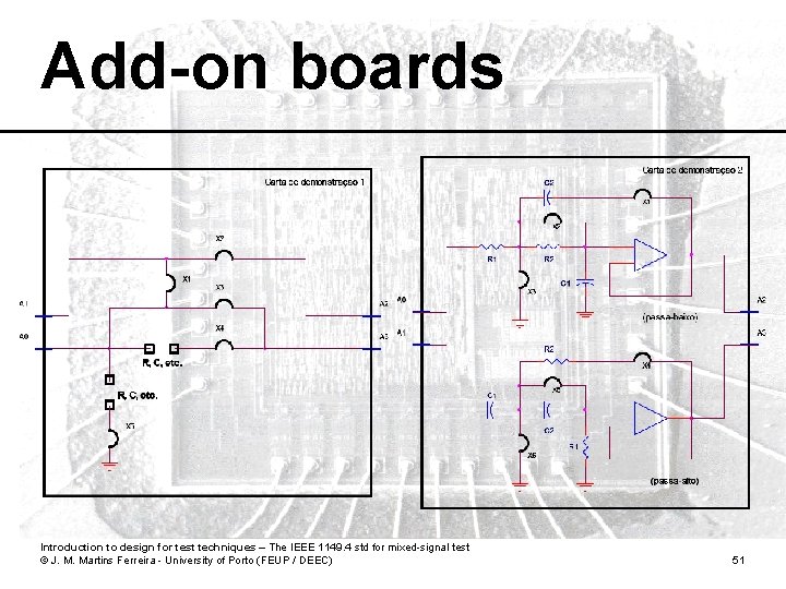
Add-on boards Introduction to design for test techniques – The IEEE 1149. 4 std for mixed-signal test © J. M. Martins Ferreira - University of Porto (FEUP / DEEC) 51

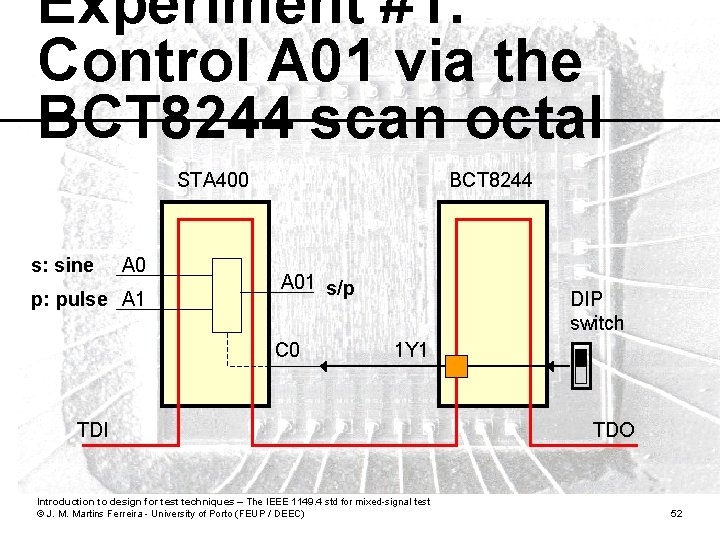
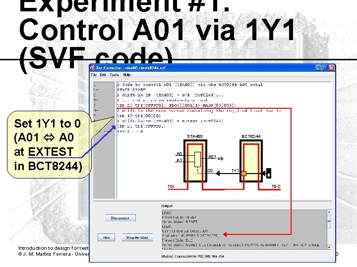
Experiment #1: Control A 01 via the BCT 8244 scan octal STA 400 s: sine A 0 p: pulse A 1 BCT 8244 A 01 s/p C 0 DIP switch 1 Y 1 TDI Introduction to design for test techniques – The IEEE 1149. 4 std for mixed-signal test © J. M. Martins Ferreira - University of Porto (FEUP / DEEC) TDO 52

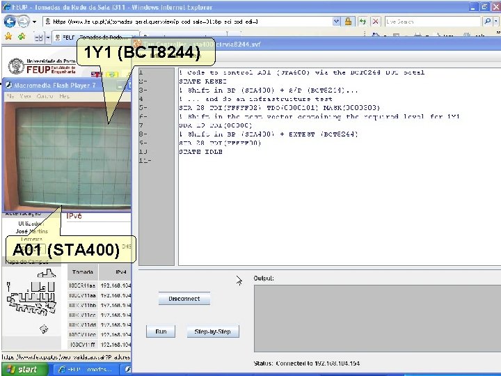
Experiment #1: Control A 01 via 1 Y 1 (SVF code) Set 1 Y 1 to 0 (A 01 A 0 at EXTEST in BCT 8244) STA 400 A 1 BCT 8244 A 01 s/p C 0 TDI Introduction to design for test techniques – The IEEE 1149. 4 std for mixed-signal test © J. M. Martins Ferreira - University of Porto (FEUP / DEEC) 1 Y 1 TDO 53

1 Y 1 (BCT 8244) A 01 (STA 400) Introduction to design for test techniques – The IEEE 1149. 4 std for mixed-signal test © J. M. Martins Ferreira - University of Porto (FEUP / DEEC) 54

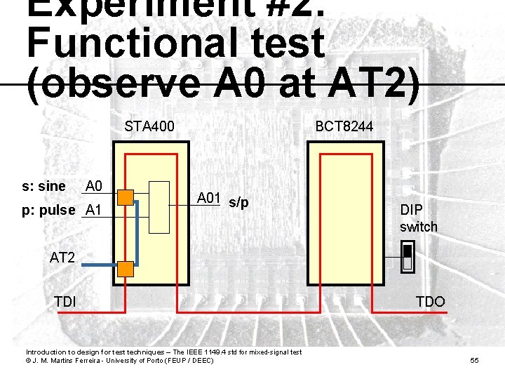
Experiment #2: Functional test (observe A 0 at AT 2) STA 400 s: sine A 0 p: pulse A 1 BCT 8244 A 01 s/p DIP switch AT 2 TDI Introduction to design for test techniques – The IEEE 1149. 4 std for mixed-signal test © J. M. Martins Ferreira - University of Porto (FEUP / DEEC) TDO 55
![Experiment 2 observe A 0 at AT 2 SVF code ABMA 0 SD Experiment #2 (observe A 0 at AT 2): SVF code ABM[A 0]: SD +](https://slidetodoc.com/presentation_image_h2/d85483f56be0a862cf639bd4304bd02c/image-56.jpg)
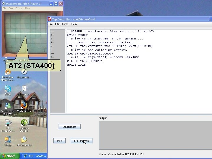
Experiment #2 (observe A 0 at AT 2): SVF code ABM[A 0]: SD + SB 2 on TBIC: S 6 + S 9 on STA 400 A 1 BCT 8244 A 01 s/p AT 2 TDI Introduction to design for test techniques – The IEEE 1149. 4 std for mixed-signal test © J. M. Martins Ferreira - University of Porto (FEUP / DEEC) TDO 56

AT 2 (STA 400) Introduction to design for test techniques – The IEEE 1149. 4 std for mixed-signal test © J. M. Martins Ferreira - University of Porto (FEUP / DEEC) 57

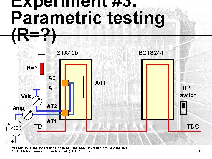
Experiment #3: Parametric testing (R=? ) STA 400 BCT 8244 R=? A 0 A 1 A 01 Volt AT 2 Amp TDI I DIP switch AT 1 TDO + Introduction to design for test techniques – The IEEE 1149. 4 std for mixed-signal test © J. M. Martins Ferreira - University of Porto (FEUP / DEEC) 58
![Experiment 3 Measuring R A 0 GND SVF code ABMA 0 SB 1 Experiment #3: Measuring R [A 0 -GND] (SVF code) ABM[A 0]: SB 1 +](https://slidetodoc.com/presentation_image_h2/d85483f56be0a862cf639bd4304bd02c/image-59.jpg)
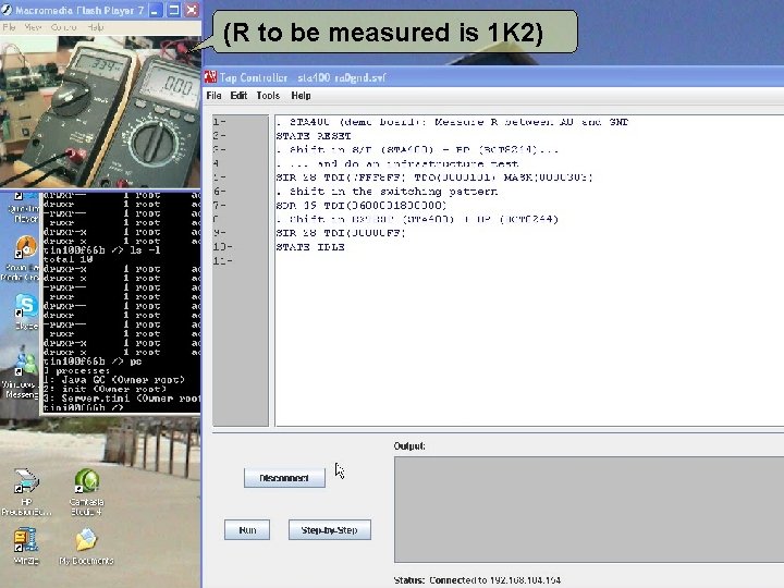
Experiment #3: Measuring R [A 0 -GND] (SVF code) ABM[A 0]: SB 1 + SB 2 on TBIC: S 5 + S 6 on STA 400 BCT 8244 R=? A 0 A 1 A 01 Volt AT 2 Amp TDI I AT 1 + Introduction to design for test techniques – The IEEE 1149. 4 std for mixed-signal test © J. M. Martins Ferreira - University of Porto (FEUP / DEEC) 59

(R to be measured is 1 K 2) Introduction to design for test techniques – The IEEE 1149. 4 std for mixed-signal test © J. M. Martins Ferreira - University of Porto (FEUP / DEEC) 60