The IBM Cell Processor Architecture and OnChip Communication

The IBM Cell Processor – Architecture and On-Chip Communication Interconnect 1
Agenda n n n Performance highlights of Cell Target applications Paper I (Cell Moves Into Limelight) Paper II (Cell Multiprocessor Communication Network) Cell Performance Overview Interconnect Usage Guidelines Real Time Enhancements Programming Model Programming Guidelines Power Management Drawbacks 2
Performance Highlights of Cell n n n Delivers 204. 8 GFlop/s single precision & 14. 6 Gflop/s double precision floating point performance Supports virtualization, large pages from the Power architecture Aggregate memory bandwidth of 25. 6 GB/s at 3. 2 GHz Configurable I/O interface capable of (raw) bandwidth of up to 25 GB/s inbound & 35 GB/s outbound Element Interconnect Bus (EIB) supports peak bandwidth of 204. 8 GB/s Extensible timers and counters to manage real- 3
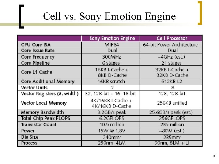
Cell vs. Sony Emotion Engine 4
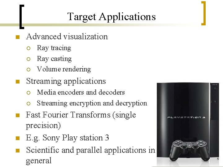
Target Applications n Advanced visualization ¡ ¡ ¡ n Streaming applications ¡ ¡ n n n Ray tracing Ray casting Volume rendering Media encoders and decoders Streaming encryption and decryption Fast Fourier Transforms (single precision) E. g. Sony Play station 3 Scientific and parallel applications in general 5
CBE Architecture - Overview n Family of processors compliant to the specifications of Broadband Processor Architecture (BPA) ¡ n n 64 bit Power architecture at the foundation Eight Synergistic Processor Elements (SPEs) Very fast on-chip Rambus XDR controller with support for two banks of Rambus XDR memory Cell processor production die has 235 m transistors and is 235 mm 2 ¡ n Designed to process media data Excludes networking peripherals or large memory arrays on chip Reaches high performance due to high clock speed and high-performance XDR DRAM interface 6
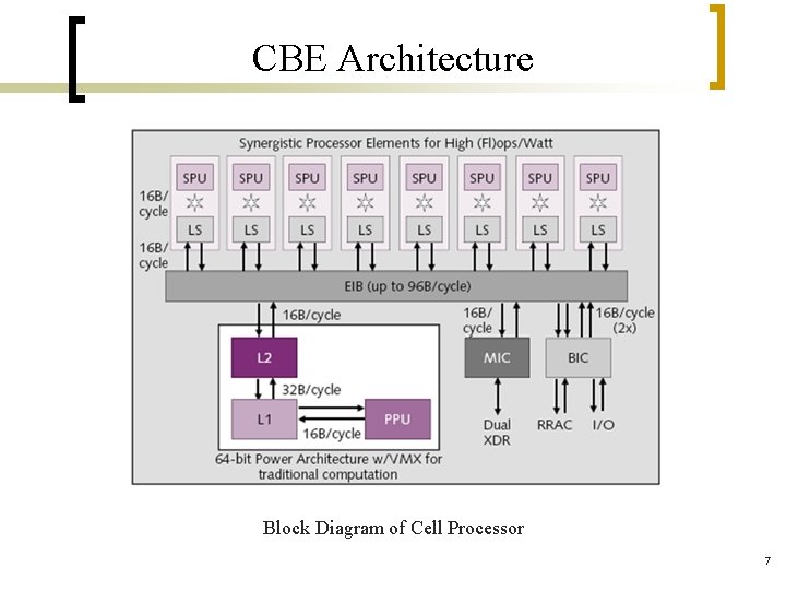
CBE Architecture Block Diagram of Cell Processor 7
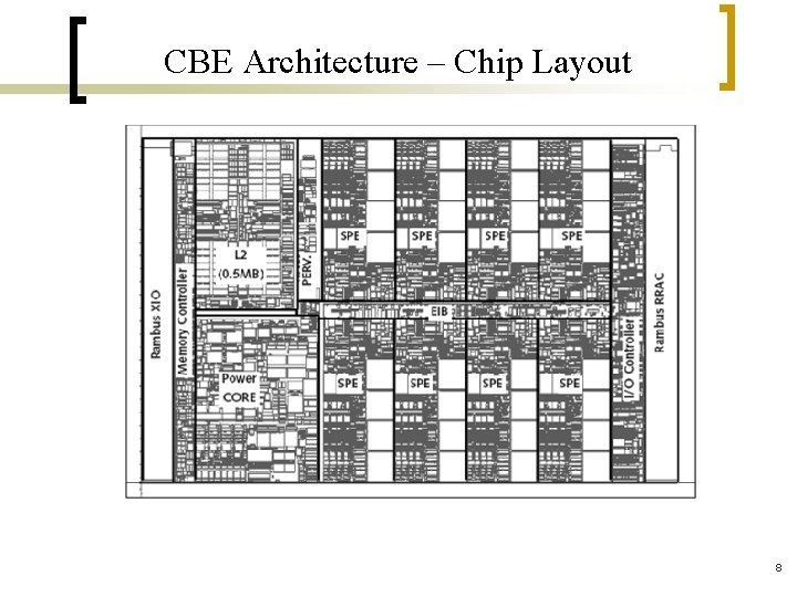
CBE Architecture – Chip Layout 8
CBE Architecture – Power Core n n n Power core + L 2 cache = Power Processing Element Includes Power with Alti. Vec (VMX) instruction set extensions In-order two issue superscalar design 21 clock cycle long pipeline Support for simultaneous (up to 2) multithreading ¡ ¡ n n n Round robin scheduling Duplicated register files, program counters and parallel instruction buffers (before decode stage) A mis-predicted branch – 8 cycle penalty Load – 4 cycle data-cache access time Big-endian processor 9
CBE Architecture – SPEs n SIMD-RISC instruction set - 4 way SIMD capability ¡ ¡ n 128 -entry 128 bit unified register file for all data types ¡ ¡ n n n Inspired by VMX/Alti. Vec instruction extensions Supports multiply-add operation with 3 sources and 1 destination Hold more data values closer to the SIMD unit Reduces the need for LS accesses “Branch hint” instructions instead of branch prediction logic in hardware – Software controlled branch prediction Can perform load, store, shuffle, channel or branch operation in parallel with a computation No multi-threading ¡ Avoids miss penalty by having all data present all the time 10
![CBE Architecture – SPEs [2] SPE is capable of limited dual issue operation Improper CBE Architecture – SPEs [2] SPE is capable of limited dual issue operation Improper](http://slidetodoc.com/presentation_image_h2/f4a07bebc8e995f789d096cb4e8c9171/image-11.jpg)
CBE Architecture – SPEs [2] SPE is capable of limited dual issue operation Improper alignment of instruction causes a swap operation forcing single-issue 11
CBE Architecture – Memory Model n PPE ¡ ¡ n 256 KB local store on SPE, 6 cycle load latency ¡ ¡ n n n 32 K 2 -way instruction cache and 32 K 4 -way set associative data cache 512 K on-chip L 2 cache Software must manage data in and out of local store Controlled by the memory flow controller Does not participate in hardware cache coherency Aliased in the memory map of the processor PPE can load and store from a memory location mapped to the local store (slow) SPE can use the DMA controller to move data to its own or other SPEs local store & between local store and main memory as well as I/O interfaces Memory flow controller on SPE can begin to transfer the data set of the next task as present one is running – Double 12
![CBE Architecture – Memory Model [2] n Only quad-word transfers from the SPE local CBE Architecture – Memory Model [2] n Only quad-word transfers from the SPE local](http://slidetodoc.com/presentation_image_h2/f4a07bebc8e995f789d096cb4e8c9171/image-13.jpg)
CBE Architecture – Memory Model [2] n Only quad-word transfers from the SPE local store ¡ n n Single ported DMA transfers support 1024 -bit transfers with quad word enables Local store supports both a wide 128 byte and a narrow 16 byte access DMA reads occupy single cycle for 128 bytes Access to local store is prioritized ¡ ¡ ¡ DMA transfers of PPE transfers occupy highest priority SPE loads and stores occupy second highest priority SPE instruction prefetch gets lowest priority 13
Memory Flow Controller (MFC) n Local to each SPU, connects it to EIB ¡ ¡ ¡ n SPU MFC via unidirectional SPU channel Separate read/write channels Each channel – unidirectional queue of varying depth configurable as blocking or non-blocking Supports about 128 outstanding requests to memory Has its own MMU Supports 64 bit virtual address and same page sizes as the power core MFC runs at the same frequency as EIB 14
![Memory Flow Controller [2] n n Accepts and processes DMA commands issued by SPU/PPE Memory Flow Controller [2] n n Accepts and processes DMA commands issued by SPU/PPE](http://slidetodoc.com/presentation_image_h2/f4a07bebc8e995f789d096cb4e8c9171/image-15.jpg)
Memory Flow Controller [2] n n Accepts and processes DMA commands issued by SPU/PPE using the channel interface or memory mapped I/O (MMIO) registers asynchronously Controller supports scatter gather and interleaved operations Supports naturally aligned transfers of 1, 2, 4, or 8 bytes or a multiple of 16 bytes to a max of 16 KB DMA list – up to 2048 DMA transfers usingle MFC DMA command 15
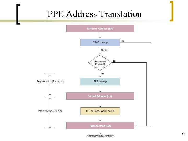
PPE Address Translation 16
CBE Architecture – Communication n Element Interconnect Bus ¡ ¡ ¡ A data-ring structure with a control bus Each ring is 16 B wide and runs at half of core clock frequency allowing 3 concurrent data transfers as long as their paths don’t overlap Four unidirectional rings, two running in each direction n ¡ ¡ Implies worst case latency of only half the distance of the ring Manages token transactions Separate communication path for command data Each bus element connected through a p 2 p link to the address concentrator Arbiter takes care of scheduling transfer ensuring no interference with in-flight transactions, gives priority to MFC and rest round robin 17
![CBE Architecture – Communication [2] Element Interconnect Bus 18 CBE Architecture – Communication [2] Element Interconnect Bus 18](http://slidetodoc.com/presentation_image_h2/f4a07bebc8e995f789d096cb4e8c9171/image-18.jpg)
CBE Architecture – Communication [2] Element Interconnect Bus 18
![CBE Architecture – Communication [3] n n n I/O can be configured as two CBE Architecture – Communication [3] n n n I/O can be configured as two](http://slidetodoc.com/presentation_image_h2/f4a07bebc8e995f789d096cb4e8c9171/image-19.jpg)
CBE Architecture – Communication [3] n n n I/O can be configured as two logical interfaces MMIO for easy access of I/O from PPE and SPE Interrupts from SPE and memory flow controller events are treated as external interrupts to PPE Two cell processors can be connected via IOIF 0 to form one coherent Cell domain using BIF protocol Signal notification - two channels Mailboxes – 32 bit communication channel between PPE and SPE ¡ ¡ n Four entry, read blocking inbound Two single entry, write blocking outbound Special operations to support synchronization mechanism 19
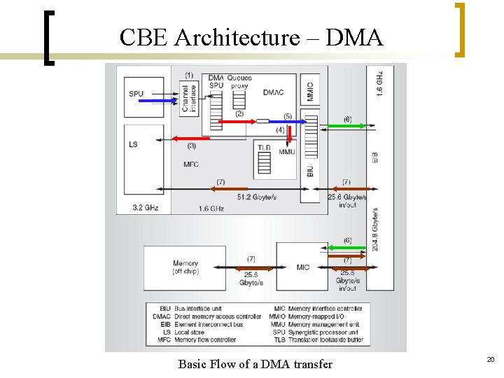
CBE Architecture – DMA Basic Flow of a DMA transfer 20
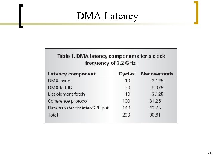
DMA Latency 21
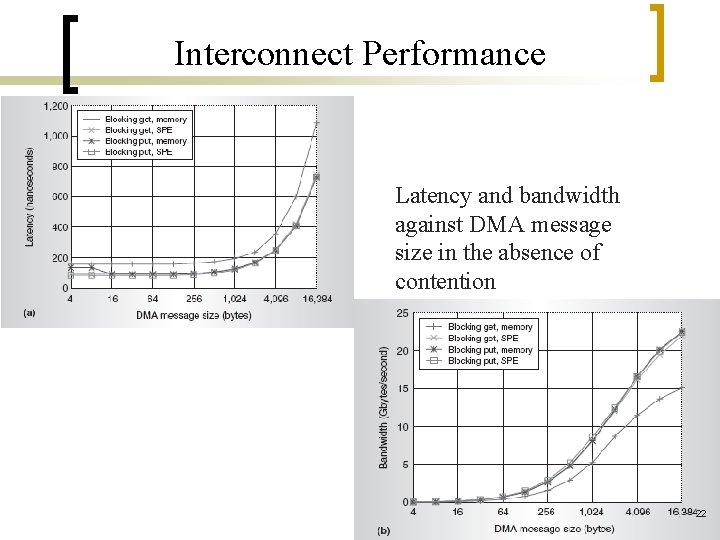
Interconnect Performance Latency and bandwidth against DMA message size in the absence of contention 22
![Interconnect Performance [2] 23 Interconnect Performance [2] 23](http://slidetodoc.com/presentation_image_h2/f4a07bebc8e995f789d096cb4e8c9171/image-23.jpg)
Interconnect Performance [2] 23
![Interconnect Performance [3] 24 Interconnect Performance [3] 24](http://slidetodoc.com/presentation_image_h2/f4a07bebc8e995f789d096cb4e8c9171/image-24.jpg)
Interconnect Performance [3] 24
![Interconnect Performance [4] 25 Interconnect Performance [4] 25](http://slidetodoc.com/presentation_image_h2/f4a07bebc8e995f789d096cb4e8c9171/image-25.jpg)
Interconnect Performance [4] 25
![Interconnect Performance [5] 26 Interconnect Performance [5] 26](http://slidetodoc.com/presentation_image_h2/f4a07bebc8e995f789d096cb4e8c9171/image-26.jpg)
Interconnect Performance [5] 26
Interconnect Usage Guidelines n n n n Bus transfers between close-by elements are faster DMA transfers can happen between any element on chip Latency for fetching up to 512 B from and to local store and main memory is not that high. Larger DMA transfers achieve higher bandwidth Non-blocking DMA operations (up to 16 per SPE and 128 overall on chip) achieve unprecedented level of parallelism Batching is very effective for intermediate DMA sizes between 256 B and 4 KB ¡ Factor of 2 or even 3 increase in bandwidth compared to the blocking case SPEs numerically consecutive may not be physically adjacent to each other on the Cell hardware layout Direction of data transfer affects performance depending on overall contention 27
Real Time Enhancements n Resource Reservation system for reserving bandwidth on shared units such as system memory, I/O interfaces n L 2 Cache Locking system based on Effective or Real Address ranges ¡ Supports both locking for Streaming, and locking for High Reuse n TLB Locking system based on Effective or Real Address ranges or DMA class. n Fully preemptible context switching capability for each SPE n Privileged Attention Event to SPE for use in 28
![Real Time Enhancements [2] n Multiple concurrent large page support in the PPE and Real Time Enhancements [2] n Multiple concurrent large page support in the PPE and](http://slidetodoc.com/presentation_image_h2/f4a07bebc8e995f789d096cb4e8c9171/image-29.jpg)
Real Time Enhancements [2] n Multiple concurrent large page support in the PPE and SPE to minimize real-time impact due to TLB misses n Up to 4 service classes (software controlled) for DMA commands (improves parallelism) n Large page I/O Translation facility for I/O devices, graphics subsystems, etc - minimizes I/O translation cache misses n SPE Event Handling facilities for high priority task notification n PPE SMT Thread priority controls for Low, Medium and High Priority Instruction dispatch 29
CBE Programming n n Tool chain for Cell built on Power. PC Linux Programming of SPE based on C with limited C++ support Debugging tools include extensions for PTrance and extended GNU debugger (GDB) Programming Models: ¡ ¡ ¡ Pipeline model Parallel model Combination of the two 30
Programming Guidelines n Each SPU be assigned a task that is allowed to run to completion of the task ¡ n n n High context switch overhead due to large number of wide registers and memory translation buffers Data transfers of size less that 128 B from the MFC are discouraged Loop unrolling is advisable on the SPEs due to heavy branch mispredict penalty PPE and SPE interaction is faster through mailboxes and signal notifications 31
Power Management n n Capable of being clocked at one-eighth the normal speed when idling Multiple power management states available to privileged software ¡ ¡ Active, slow, pause, state retained and isolated (SRI), state lost and isolated (SLI) Each progressively more aggressive in saving power Software controls the transitions, but can be linked to external events SLI state – the device is effectively shut off from the system 32
Drawbacks n Full SPE context switch is relatively expensive ¡ n This can negatively affect virtualization of SPEs if not properly handled This instantiation of Cell – not suitable for DP math ¡ ¡ ¡ The IEEE correctness is sacrificed for speed and simplicity since present version is geared for media applications No support for IEEE 754 precise mode Use by super computer applications will require further development 33
![References [1] Kewin Krewell. "Cell Moves Into The Limelight". Microprocessor {2/14/05 -01} [2] Michael References [1] Kewin Krewell. "Cell Moves Into The Limelight". Microprocessor {2/14/05 -01} [2] Michael](http://slidetodoc.com/presentation_image_h2/f4a07bebc8e995f789d096cb4e8c9171/image-34.jpg)
References [1] Kewin Krewell. "Cell Moves Into The Limelight". Microprocessor {2/14/05 -01} [2] Michael Kistler, Michael Perrone, Fabrizio Petrini. "Cell Multiprocessor Communication Network: Built For Speed". In IEEE Micro, 26(3), May/June 2006 [3] Cell Broadband Engine resource center. http: //www 128. ibm. com/developerworks/power/cell/ [4] H. Peter Hofstee. “Introduction to Cell Broadband Engine” 34
- Slides: 34