The High Resolution Array is a detector designed
- Slides: 13

The High Resolution Array is a detector designed to detect and identify light charged particles like protons, deuterium, triton, alpha's and the different isotopes of nuclei with Z<10. These are particles that are produced in nuclear reactions, and by obtaining an accurate measurement of their direction and energy we can learn much about the dynamics of nuclear reactions and the structure of nuclei. This project is a collaboration between the National Superconducting Cyclotron Laboratory, Michigan State University, Chemistry department, Indiana University, Washington University, St. Louis (MO) and INFN, Milan, Italy. [Click anywhere in the slides to continue the slideshow]

Some of the Physics Addressed with Hi. RA was designed with radioactive beam facilities like the Coupled Cyclotron Facility at NSCL/MSU in mind. - Multifragmentation - Transfer reactions (p, d), (d, p), (a, t), … - Resonance spectroscopy - Inverse Kinematics Measurements - Radiative Capture via Coulomb dissociation. - Elastic and Inelastic Scattering in reverse kinematics (p, p’), (a, a), … This defines performance goals <0. 3 , E<50 ke. V (E<20 Me. V)

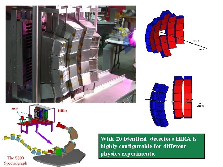
With 20 Identical detectors Hi. RA is highly configurable for different physics experiments.

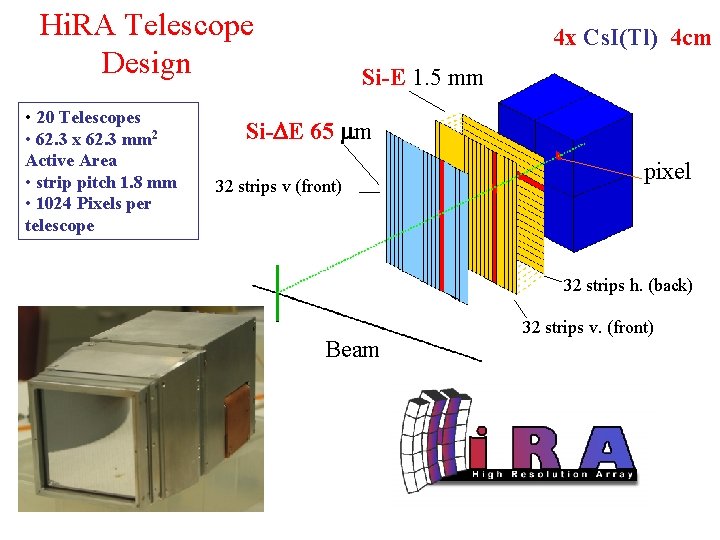
Hi. RA Telescope Design • 20 Telescopes • 62. 3 x 62. 3 mm 2 Active Area • strip pitch 1. 8 mm • 1024 Pixels per telescope 4 x Cs. I(Tl) 4 cm Si-E 1. 5 mm Si-DE 65 mm 32 strips v (front) pixel 32 strips h. (back) Beam 32 strips v. (front)

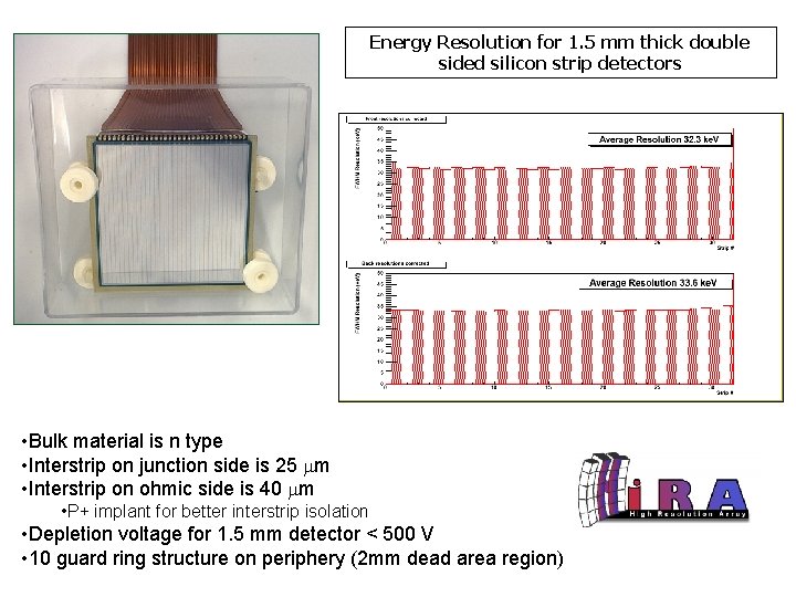
Energy Resolution for 1. 5 mm thick double sided silicon strip detectors • Bulk material is n type • Interstrip on junction side is 25 mm • Interstrip on ohmic side is 40 mm • P+ implant for better interstrip isolation • Depletion voltage for 1. 5 mm detector < 500 V • 10 guard ring structure on periphery (2 mm dead area region)

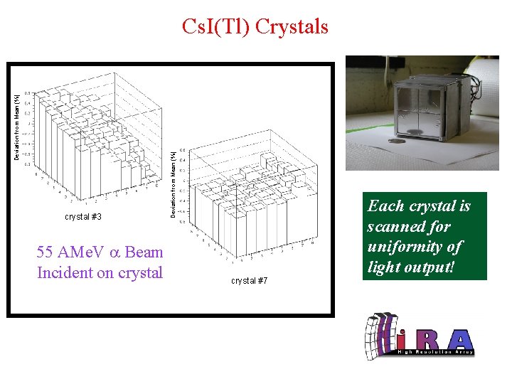
crystal #3 55 AMe. V a Beam Incident on crystal Deviation from Mean (%) Cs. I(Tl) Crystals crystal #7 Each crystal is scanned for uniformity of light output!

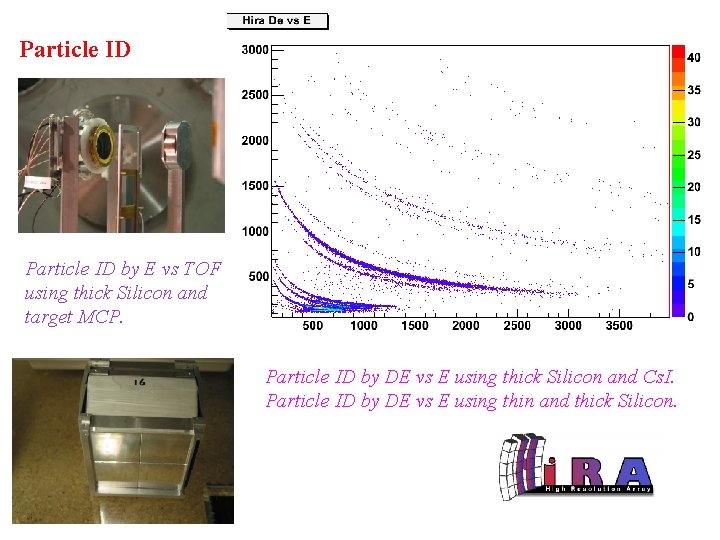
Particle ID by E vs TOF using thick Silicon and target MCP. Particle ID by DE vs E using thick Silicon and Cs. I. Particle ID by DE vs E using thin and thick Silicon.

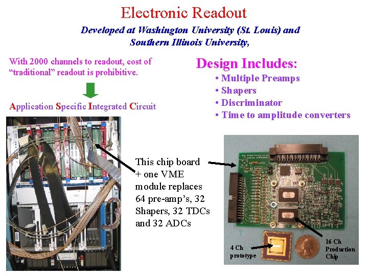
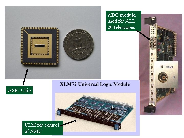
Electronic Readout Developed at Washington University (St. Louis) and Southern Illinois University, With 2000 channels to readout, cost of “traditional” readout is prohibitive. Design Includes: Application Specific Integrated Circuit • Multiple Preamps • Shapers • Discriminator • Time to amplitude converters This chip board + one VME module replaces 64 pre-amp’s, 32 Shapers, 32 TDCs and 32 ADCs 4 Ch prototype 16 Ch Production Chip

ADC module, used for ALL 20 telescopes ASIC Chip ULM for control of ASIC

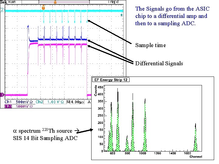
The Signals go from the ASIC chip to a differential amp and then to a sampling ADC. Sample time Differential Signals a spectrum 228 Th source SIS 14 Bit Sampling ADC

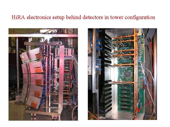
Hi. RA electronics setup behind detectors in tower configuration

The Hi. RA collaboration (as of 2005) MSU / NSCL • Bill Lynch • Betty. Tsang • Mark Wallace • M-J. van Goethem • Mike Famiano • Franck Delaunay • Michal Mocko • Andy Rogers • B. Nett • D. Oostdyke • S. Simpson • J. K • J. Veazey • Shawn Tornga • Jacob Clifford • Sergei Lukyanov IU / IUCF • RT. de Souza • A. L. Caraley • B. P. Davin • R. Alfaro-Molina • S. Hudan • V. Viola • Carlos INFN Milano • A. Moroni Washingon Univiersity, St. Louis • L. Sobotka • R. Charity • J. M. Elson Southern Illinois University, Edwardsville • G. L. Engel

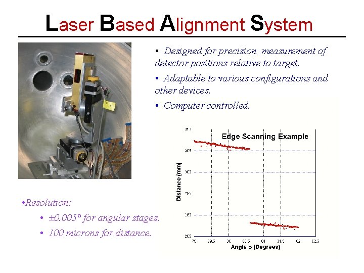
Laser Based Alignment System • Designed for precision measurement of detector positions relative to target. • Adaptable to various configurations and other devices. • Computer controlled. • Resolution: • ± 0. 005° for angular stages. • 100 microns for distance.