The future of solidstate transistors Jrgen Olsson Uppsala

- Slides: 28

The future of solid-state transistors Jörgen Olsson Uppsala University Sweden

Outline • Development of RF-LDMOS • High-power transistor options – VMOS – LDMOS – Ga. N • Development trend • Summary

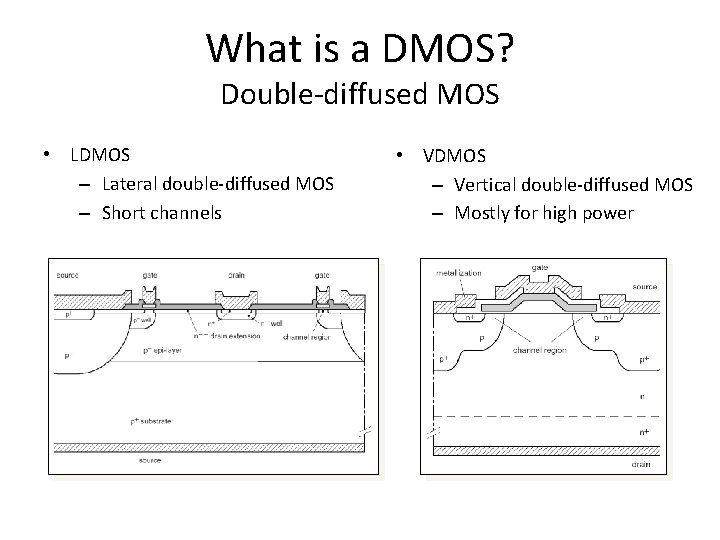
What is a DMOS? Double-diffused MOS • LDMOS – Lateral double-diffused MOS – Short channels • VDMOS – Vertical double-diffused MOS – Mostly for high power

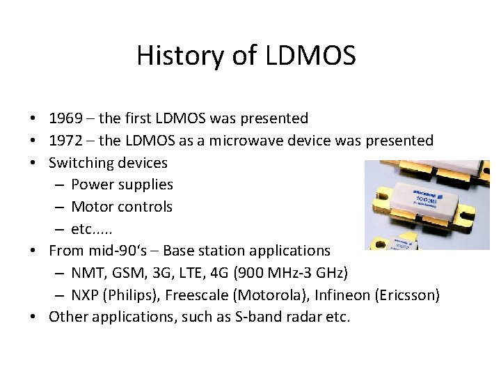
History of LDMOS • 1969 – the first LDMOS was presented • 1972 – the LDMOS as a microwave device was presented • Switching devices – Power supplies – Motor controls – etc. . . • From mid-90‘s – Base station applications – NMT, GSM, 3 G, LTE, 4 G (900 MHz-3 GHz) – NXP (Philips), Freescale (Motorola), Infineon (Ericsson) • Other applications, such as S-band radar etc.

RF-LDMOS 28 V • Major development has been with focus on parameters important for mobile communications, such as gain, efficiency, linearity, increased operation frequency. • Other advantages: high reliability, low-cost package with ground on chip back-side (low inductance and resistance)

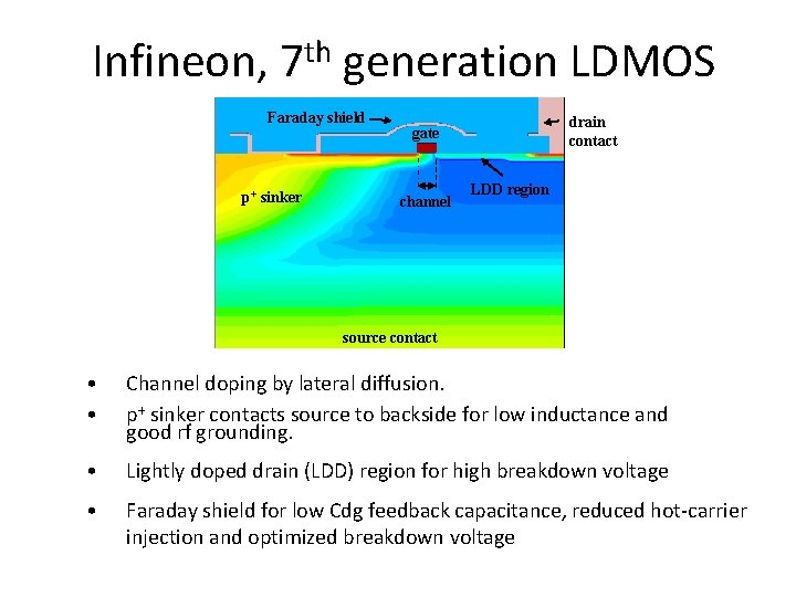
Infineon, th 7 generation LDMOS Faraday shield p+ sinker drain contact gate channel LDD region source contact • • Channel doping by lateral diffusion. p+ sinker contacts source to backside for low inductance and good rf grounding. • Lightly doped drain (LDD) region for high breakdown voltage • Faraday shield for low Cdg feedback capacitance, reduced hot-carrier injection and optimized breakdown voltage

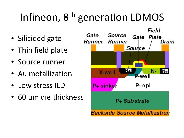
Infineon, 8 th generation LDMOS • • • Silicided gate Thin field plate Source runner Au metallization Low stress ILD 60 um die thickness

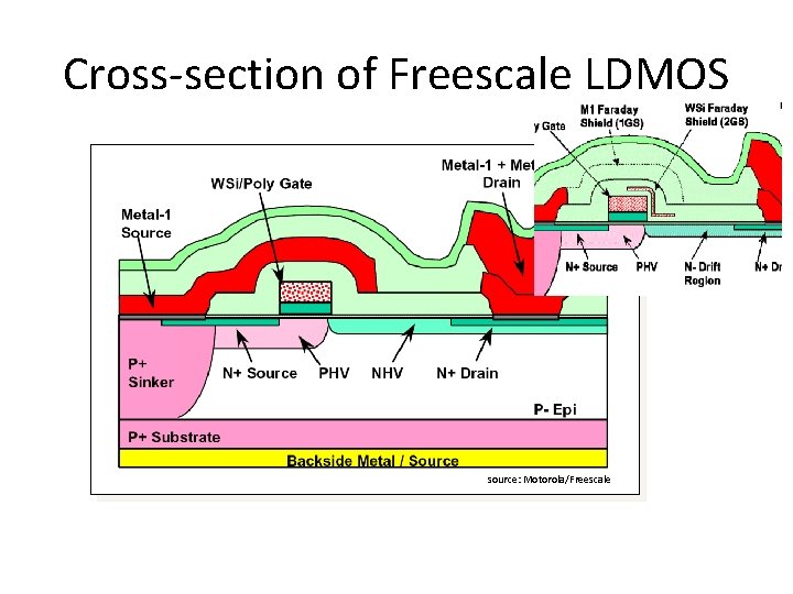
Cross-section of Freescale LDMOS source: Motorola/Freescale

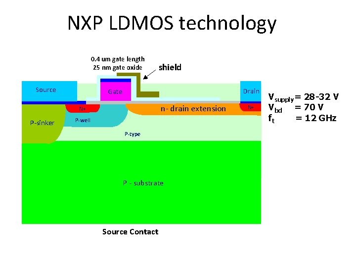
NXP LDMOS technology 0. 4 um gate length 25 nm gate oxide Source Drain Gate n- drain extension N+ P-sinker shield P-well P-type P- substrate P - substrate Source Contact N+ SN Vsupply= 28 -32 V Vbd = 70 V ft = 12 GHz

Example: 100 W transistor Drain Inshing MOSCapacitor LDMOS-die BL N F 6 XP G 3 85 0 Gate Advantage: on-chip matching Prematch MOScapacitor

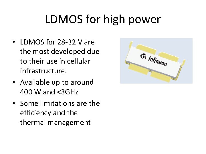
LDMOS for high power • LDMOS for 28 -32 V are the most developed due to their use in cellular infrastructure. • Available up to around 400 W and <3 GHz • Some limitations are the efficiency and thermal management

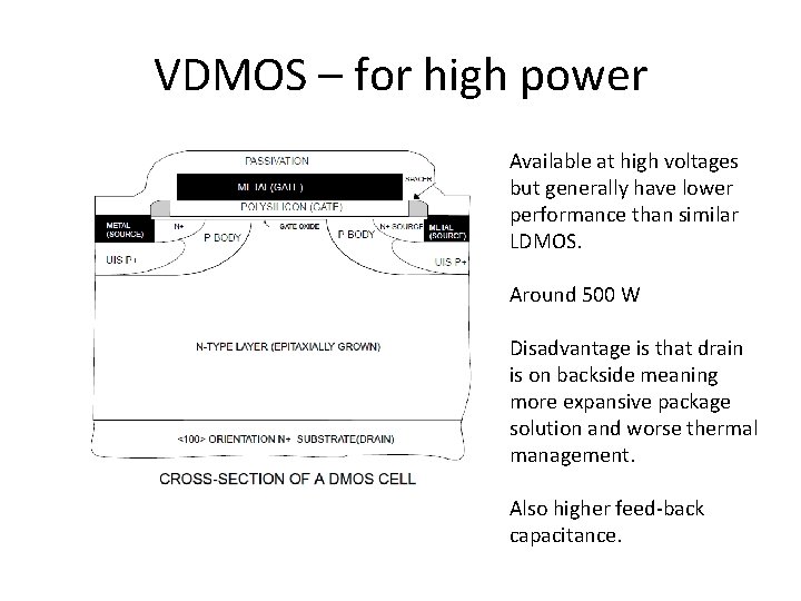
VDMOS – for high power Available at high voltages but generally have lower performance than similar LDMOS. Around 500 W Disadvantage is that drain is on backside meaning more expansive package solution and worse thermal management. Also higher feed-back capacitance.

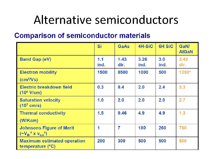
Alternative semiconductors

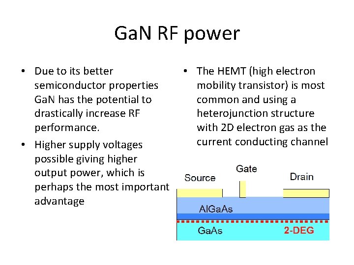
Ga. N RF power • Due to its better semiconductor properties Ga. N has the potential to drastically increase RF performance. • Higher supply voltages possible giving higher output power, which is perhaps the most important advantage • The HEMT (high electron mobility transistor) is most common and using a heterojunction structure with 2 D electron gas as the current conducting channel

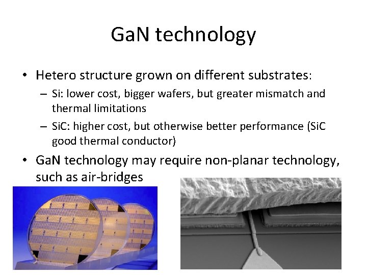
Ga. N technology • Hetero structure grown on different substrates: – Si: lower cost, bigger wafers, but greater mismatch and thermal limitations – Si. C: higher cost, but otherwise better performance (Si. C good thermal conductor) • Ga. N technology may require non-planar technology, such as air-bridges

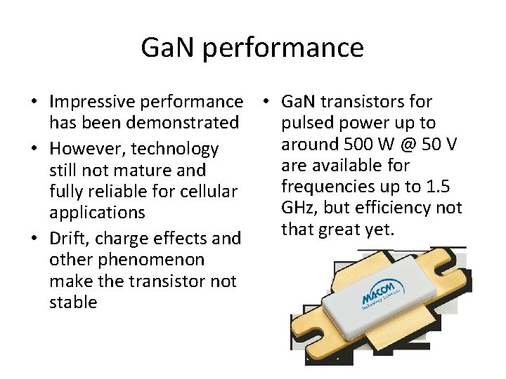
Ga. N performance • Impressive performance • Ga. N transistors for has been demonstrated pulsed power up to around 500 W @ 50 V • However, technology are available for still not mature and frequencies up to 1. 5 fully reliable for cellular GHz, but efficiency not applications that great yet. • Drift, charge effects and other phenomenon make the transistor not stable

Development trends • The use of e. g. SMPA in cellular, motivated by higher efficiencies, has driven technology towards higher supply voltages • Present 28 V not easily scaled to higher voltages – new concepts may be needed • Major players, such as NXP, Freescale and Infineon now have 50 V LDMOS technology, mainly targeting applications outside the cellular infrastructure

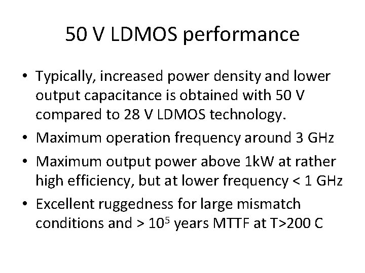
50 V LDMOS performance • Typically, increased power density and lower output capacitance is obtained with 50 V compared to 28 V LDMOS technology. • Maximum operation frequency around 3 GHz • Maximum output power above 1 k. W at rather high efficiency, but at lower frequency < 1 GHz • Excellent ruggedness for large mismatch conditions and > 105 years MTTF at T>200 C

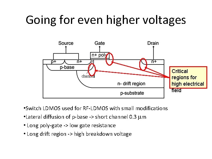
Going for even higher voltages channel • Switch LDMOS used for RF-LDMOS with small modifications • Lateral diffusion of p-base -> short channel 0. 3 mm • Long poly-gate -> low gate resistance • Long drift region -> high breakdown voltage Critical regions for high electrical field

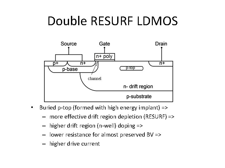
Double RESURF LDMOS channel • Buried p-top (formed with high energy implant) => – more effective drift region depletion (RESURF) => – higher drift region (n-well) doping => – lower resistance for almost preserved BV => – higher drive current

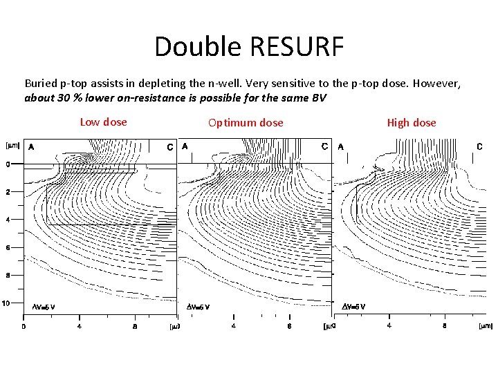
Double RESURF Buried p-top assists in depleting the n-well. Very sensitive to the p-top dose. However, about 30 % lower on-resistance is possible for the same BV Low dose Optimum dose High dose

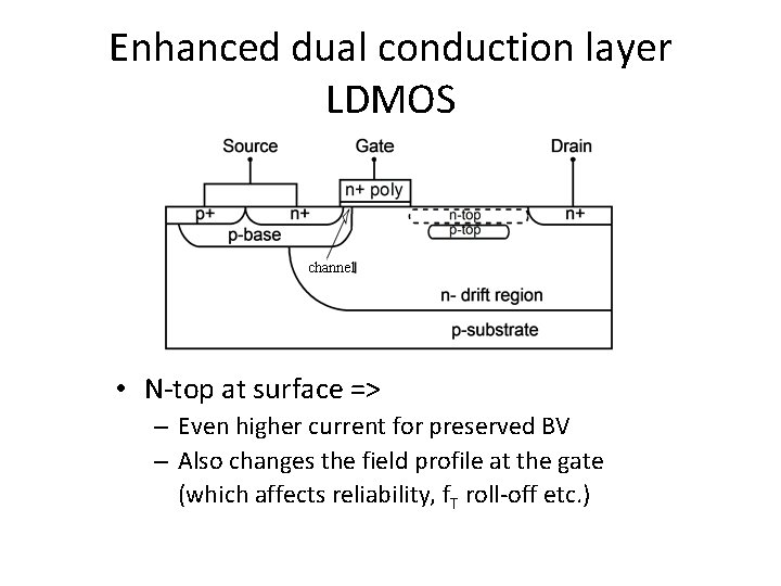
Enhanced dual conduction layer LDMOS channel • N-top at surface => – Even higher current for preserved BV – Also changes the field profile at the gate (which affects reliability, f. T roll-off etc. )

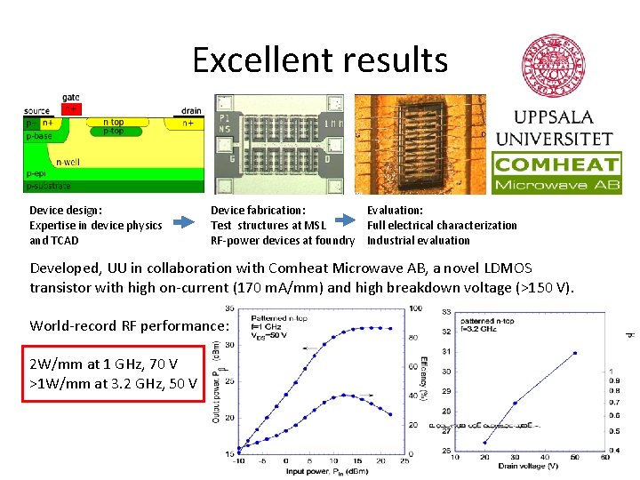
Excellent results Device design: Expertise in device physics and TCAD Device fabrication: Evaluation: Test structures at MSL Full electrical characterization RF-power devices at foundry Industrial evaluation Developed, UU in collaboration with Comheat Microwave AB, a novel LDMOS transistor with high on-current (170 m. A/mm) and high breakdown voltage (>150 V). World-record RF performance: 2 W/mm at 1 GHz, 70 V >1 W/mm at 3. 2 GHz, 50 V

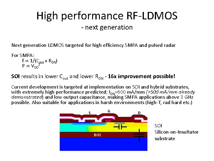
High performance RF-LDMOS - next generation Next generation LDMOS targeted for high efficiency SMPA and pulsed radar For SMPA: f 1/(Cout x RON) P VDD 2 SOI results in lower Cout and lower RON - 16 x improvement possible! Current development is targeted at implementation on SOI and hybrid substrates, with extremely high performance predicted; ION>600 m. A/mm (>500 m. A/mm already demonstrated) and low output capacitance, making SMPA applications above 3 GHz possible. Also suitable for applications in harsh environments (high-T, rad hard etc. ) G S BOX D SOI Silicon-on-Insultator substrate

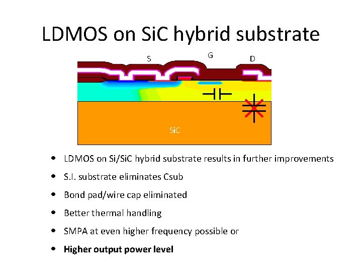
LDMOS on Si. C hybrid substrate G S D BOX Si. C • • • LDMOS on Si/Si. C hybrid substrate results in further improvements S. I. substrate eliminates Csub Bond pad/wire cap eliminated Better thermal handling SMPA at even higher frequency possible or Higher output power level

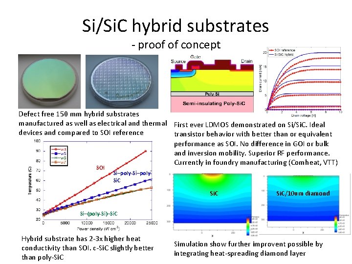
Si/Si. C hybrid substrates - proof of concept Defect free 150 mm hybrid substrates manufactured as well as electrical and thermal First ever LDMOS demonstrated on Si/Si. C. Ideal devices and compared to SOI reference transistor behavior with better than or equivalent performance as SOI. No difference in GOI or bulk and inversion mobility. Superior RF performance. Currently in foundry manufacturing (Comheat, VTT) SOI Si–poly-Si–poly. Si. C/10 um diamond Si–(poly-Si)–Si. C Hybrid substrate has 2 -3 x higher heat conductivity than SOI. c-Si. C slightly better than poly-Si. C Simulation show further improvent possible by integrating heat-spreading diamond layer

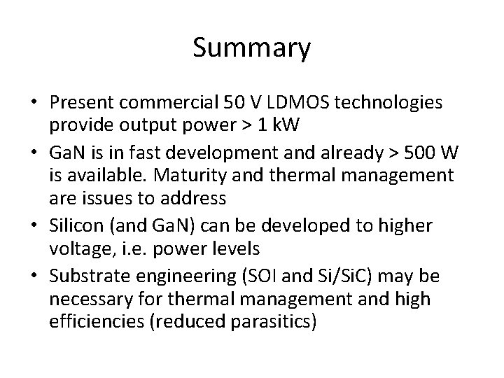
Summary • Present commercial 50 V LDMOS technologies provide output power > 1 k. W • Ga. N is in fast development and already > 500 W is available. Maturity and thermal management are issues to address • Silicon (and Ga. N) can be developed to higher voltage, i. e. power levels • Substrate engineering (SOI and Si/Si. C) may be necessary for thermal management and high efficiencies (reduced parasitics)

Acknowledgments • Some material shown with courtesy of: