The Fundamentals of Photochemical Machining PCM for Engineers
- Slides: 57

The Fundamentals of Photochemical Machining (PCM) for Engineers and College and University Students A presentation by Emeritus Professor David Allen BSc, Ph. D, DSc, FCIRP on behalf of the Photo Chemical Machining Institute (PCMI) – an international, not-for-profit, organisation for the promotion of photochemical machining technology. April 2016

What is PCM? PCM is a manufacturing process used to fabricate a very wide range of products used in aerospace, automobile, electronic, mechanical, biomedical engineering and decorative applications.

The next few slides show some examples of PCM products The little-known process of PCM - “Manufacturing’s best kept secret” had product sales of approximately US$6 billion in 2000.

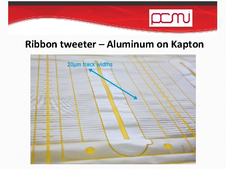
Ribbon tweeter – Aluminum on Kapton 20µm track widths

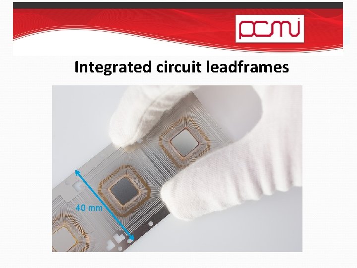
Integrated circuit leadframes 40 mm

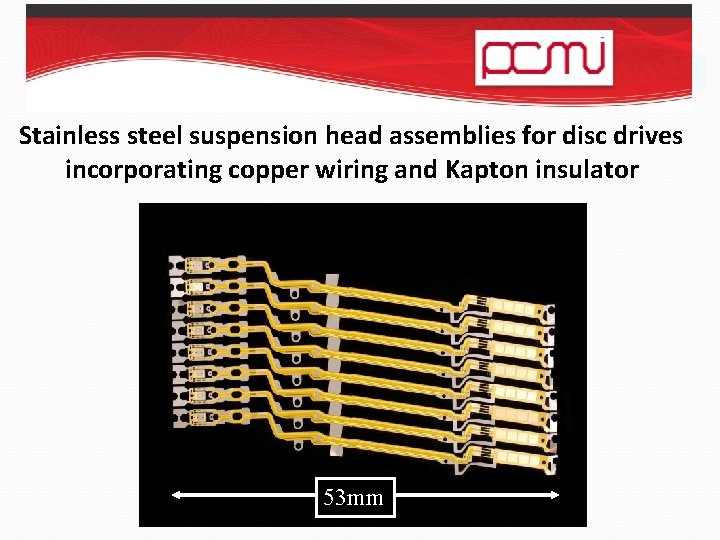
Stainless steel suspension head assemblies for disc drives incorporating copper wiring and Kapton insulator 53 mm 53 mm

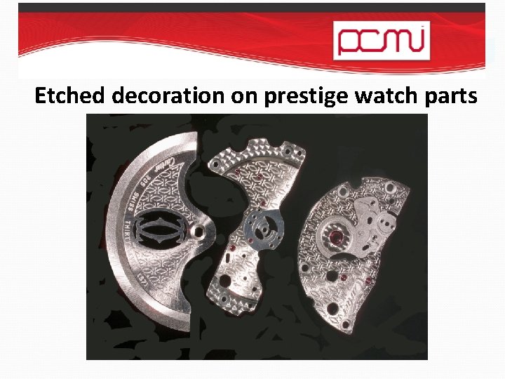
Etched decoration on prestige watch parts

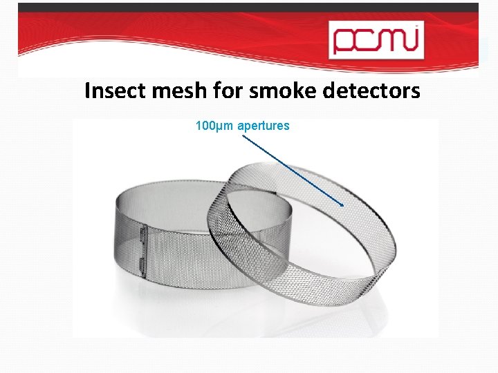
Insect mesh for smoke detectors 100µm apertures

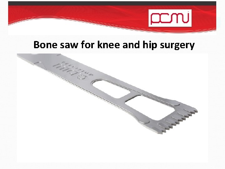
Bone saw for knee and hip surgery 100µm apertures

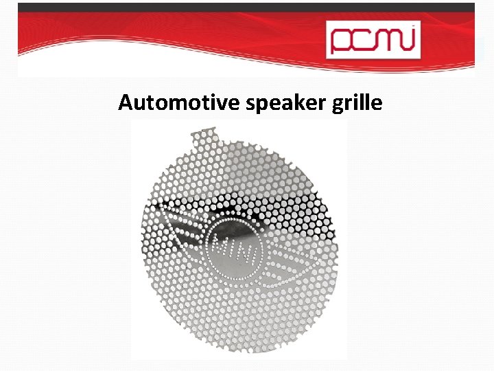
Automotive speaker grille

Other PCM products Perforated products such as: Grids, filters, meshes, screens, masks and attenuators. Complex geometry products such as: Shims, gaskets, levers, diaphragms, washers, springs, links, brackets, connectors, probes, heat sinks and exchangers, lead frames, rotor and stator laminations, shutter blades, iris leaves, graticules, masks, encoder discs, jewellery. Surface-etched products such as: Rules, scales, clutch plates, emitter contacts, bearings, edge filters, hybrid circuit pack lids, boxes and enclosures, nameplates, decorative plaques, components etched with permanent logos, trademarks, part numbers or instructions.

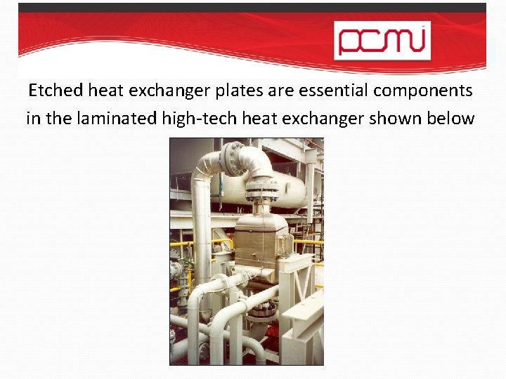
Etched heat exchanger plates are essential components in the laminated high-tech heat exchanger shown below

How are these products manufactured?

Designing PCM Products with CAD The engineering drawing is digitised to produce data streams that can be utilised to produce either: • a conventional high resolution phototool via a photoplotter or • instructions to drive a laser to expose photoresist –coated metal directly (known as Laser Direct Imaging or LDI)

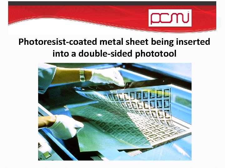
Photoresist-coated metal sheet being inserted into a double-sided phototool

What is the purpose of a photoresist? A photoresist - a uv photosensitive polymer supplied as a liquid or dry film - is used to produce an image on metal. Where the photoresist has been exposed to uv radiation, it becomes insoluble in a developer solution and adheres strongly to the metal surface to form an etchant-resistant coating.

Coating § The objective of photoresist coating is to provide a protective surface stencil that can protect from (resist) the action of chemical etching. § The stencil pattern is achieved by photo-exposure of the light-sensitive coating via uv flood exposure through a phototool or uv laser exposure (also known as laser direct imaging or LDI).

Resolution v. coating thickness § In general, liquid photoresists will give coating thicknesses between 2 m and 15 m. § Dry film photoresist thicknesses are generally between 10 m and 100 m. § The finest features will be resolved in the thinnest photoresists but the stencil gains increased strength with thicker coatings. Note the compromise

Liquid photoresists Solvent and aqueous photoresists can be applied by: § Spinning (high speed) or Whirling (low speed) § Dipping (the method most commonly used) § Spraying § Flowing § Roller coating and for conductive (largely aqueous) systems § Electrophoretic coating

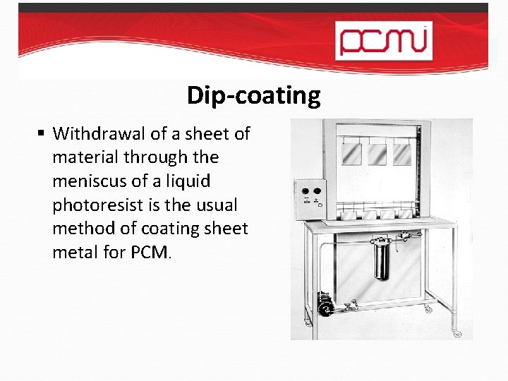
Dip-coating § Withdrawal of a sheet of material through the meniscus of a liquid photoresist is the usual method of coating sheet metal for PCM.

Dry film photoresists can be applied by hot lamination and the images developed by: § Aqueous solutions (predominant in the 21 st century) § Semi-aqueous solutions (an environmental development of the 1970 s) § Solvents (the original technology of 1960 s)

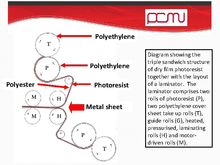
Polyethylene T Polyethylene P Polyester M Photoresist H Metal sheet M H P T Diagram showing the triple sandwich structure of dry film photoresist together with the layout of a laminator. The laminator comprises two rolls of photoresist (P), two polyethylene cover sheet take up rolls (T), guide rolls (G), heated, pressurised, laminating rolls (H) and motordriven rolls (M).

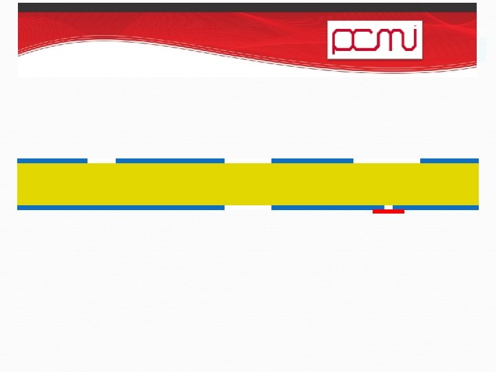
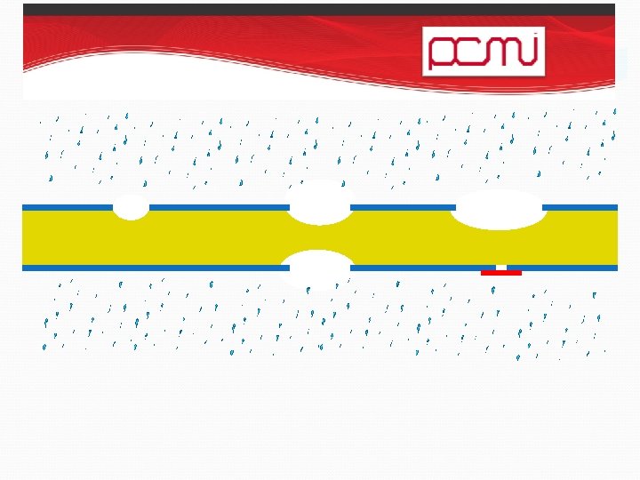
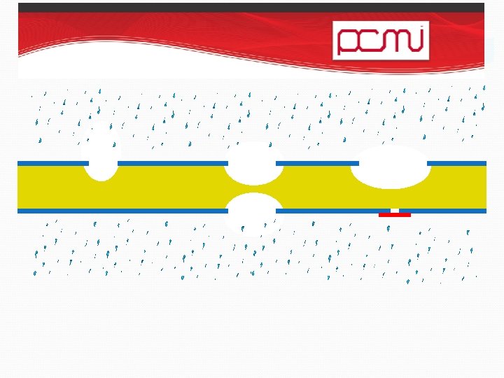
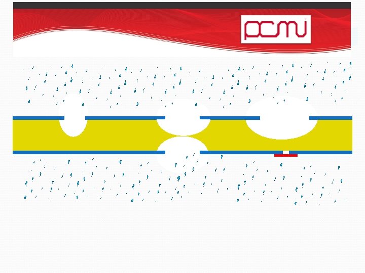
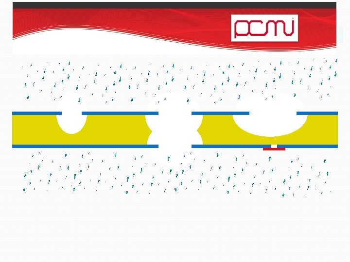
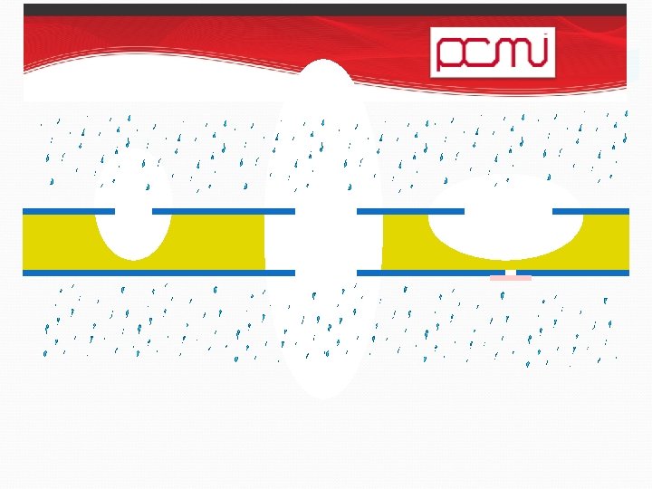
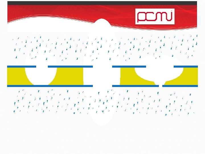
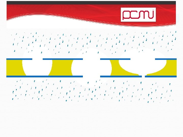
The PCM Production Process Once the photoresist has been imaged to produce an etchant –resistant patterned coating, chemical etching is used to transfer that pattern into the metal by selective removal as shown in the following animation.

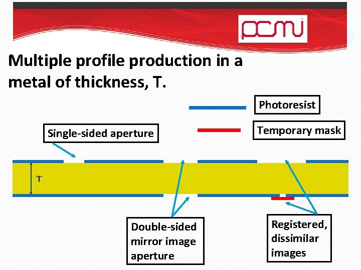
Multiple profile production in a metal of thickness, T. Photoresist Single-sided aperture Temporary mask T Double-sided mirror image aperture Registered, dissimilar images


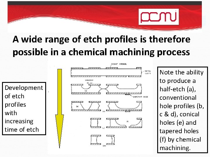
A wide range of etch profiles is therefore possible in a chemical machining process Development of etch profiles with increasing time of etch Note the ability to produce a half-etch (a), conventional hole profiles (b, c & d), conical holes (e) and tapered holes (f) by chemical machining.

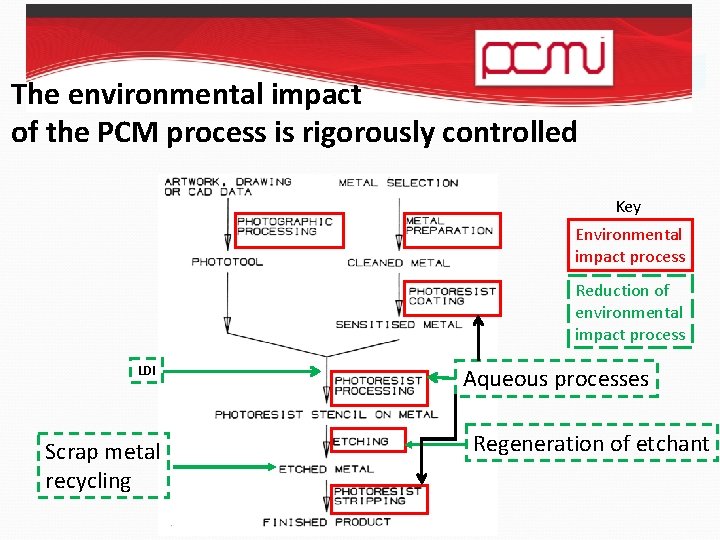
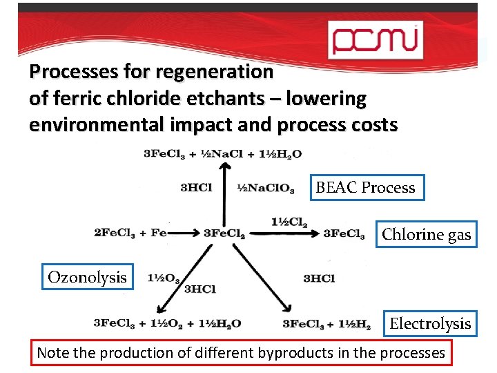
Environmental Control of PCM for “Health & Safety” and Economy All metal processing will produce some degree of environmental impact but the impact of PCM can be reduced by: § use of aqueous processing solutions instead of solvents (VOCs) § the elimination of photographic processing by using LDI § recycling of scrap metal waste and § regeneration of waste etchant. The commonest industrial etchant is an aqueous solution of ferric chloride (Fe. Cl 3). The waste product from etching metals is ferrous chloride (Fe. Cl 2). By employing strong chemical oxidising agents, the waste Fe. Cl 2 can be converted back to Fe. Cl 3 etchant (known as regeneration). This reduces both environmental impact and the cost of waste etchant disposal.

The environmental impact of the PCM process is rigorously controlled Key Environmental impact process Reduction of environmental impact process LDI Scrap metal recycling Aqueous processes Regeneration of etchant

Processes for regeneration of ferric chloride etchants – lowering environmental impact and process costs BEAC Process Chlorine gas Ozonolysis Electrolysis Note the production of different byproducts in the processes

Competing technologies: the designer needs to choose the lowest-cost manufacturing process that also meets the technical specifications of the product

Competitive processes include: Computer Numerical Control (CNC) Machining Photoelectroforming (PEF) Laser Beam Machining (LBM) Wire Electrodischarge Machining (WEDM) Stamping

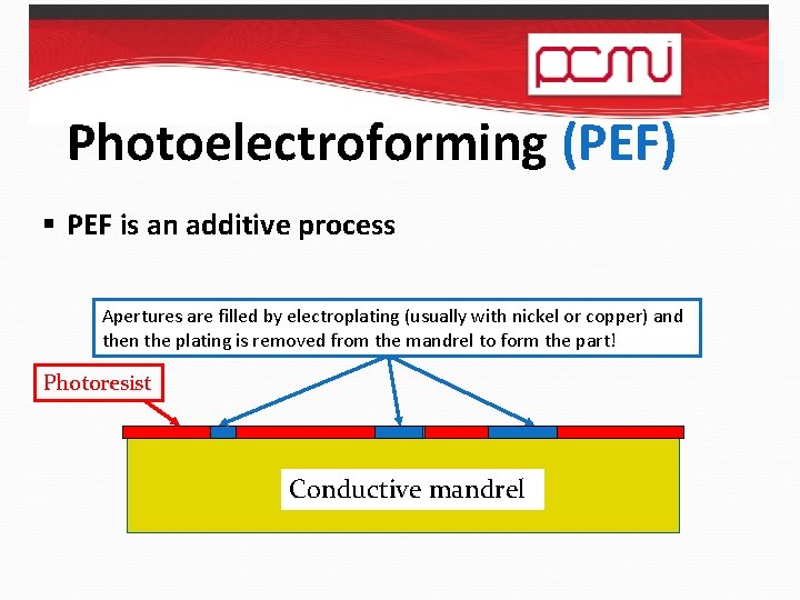
Photoelectroforming (PEF) § PEF is an additive process Apertures are filled by electroplating (usually with nickel or copper) and then the plating is removed from the mandrel to form the part! Photoresist Conductive mandrel

Laser Beam Machining (LBM) § Laser beam machining (LBM) is a thermal non-traditional machining process which uses a laser to melt and vaporise materials. § The beam can be focused for drilling holes through metals as thick as 10 mm. High energy solid state and gas lasers are needed, with the optical characteristics of the workpiece determining the wavelength of light energy that should be used.

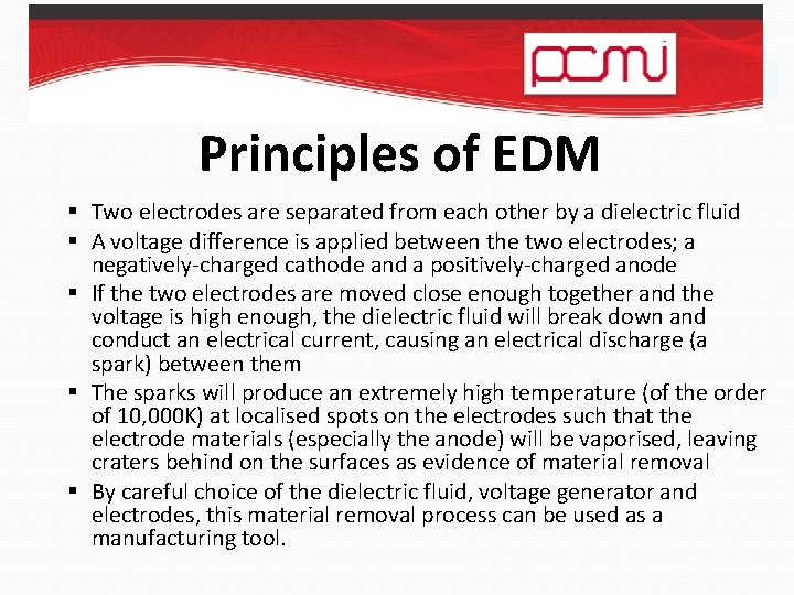
Principles of EDM § Two electrodes are separated from each other by a dielectric fluid § A voltage difference is applied between the two electrodes; a negatively-charged cathode and a positively-charged anode § If the two electrodes are moved close enough together and the voltage is high enough, the dielectric fluid will break down and conduct an electrical current, causing an electrical discharge (a spark) between them § The sparks will produce an extremely high temperature (of the order of 10, 000 K) at localised spots on the electrodes such that the electrode materials (especially the anode) will be vaporised, leaving craters behind on the surfaces as evidence of material removal § By careful choice of the dielectric fluid, voltage generator and electrodes, this material removal process can be used as a manufacturing tool.

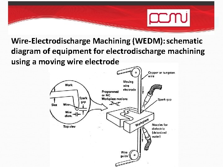
Wire-Electrodischarge Machining (WEDM): schematic diagram of equipment for electrodischarge machining using a moving wire electrode

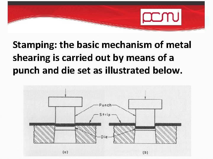
Stamping: the basic mechanism of metal shearing is carried out by means of a punch and die set as illustrated below.

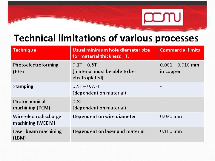
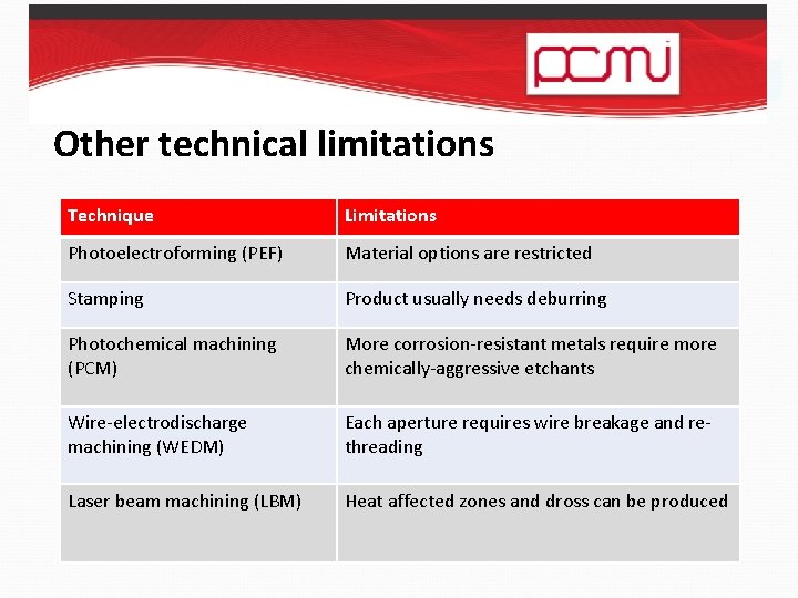
Technical limitations of these competitive manufacturing processes: Each process has some technical limitations. Can the chosen process manufacture the part you have designed?

Technical limitations of various processes Technique Usual minimum hole diameter size for material thickness , T. Commercial limits Photoelectroforming (PEF) 0. 1 T – 0. 5 T (material must be able to be electroplated) 0. 001 – 0. 010 mm in copper Stamping 0. 5 T – 0. 75 T (dependent on material) - Photochemical machining (PCM) 0. 8 T (dependent on material) - Wire-electrodischarge machining (WEDM) Dependent on wire diameter 0. 030 mm Laser beam machining (LBM) Dependent on laser and material 0. 100 mm Minimum aperture size

Other technical limitations Technique Limitations Photoelectroforming (PEF) Material options are restricted Stamping Product usually needs deburring Photochemical machining (PCM) More corrosion-resistant metals require more chemically-aggressive etchants Wire-electrodischarge machining (WEDM) Each aperture requires wire breakage and rethreading Laser beam machining (LBM) Heat affected zones and dross can be produced

Economic comparisons

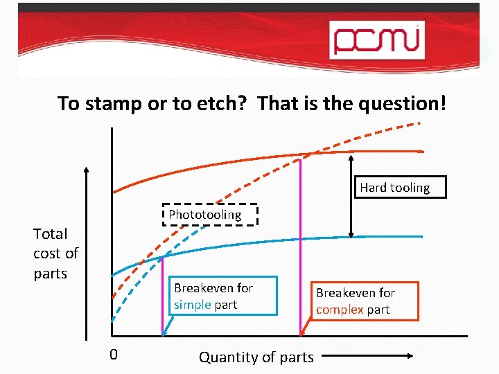
To stamp or to etch? That is the question! Hard tooling Phototooling Total cost of parts Breakeven for simple part 0 Quantity of parts Breakeven for complex part

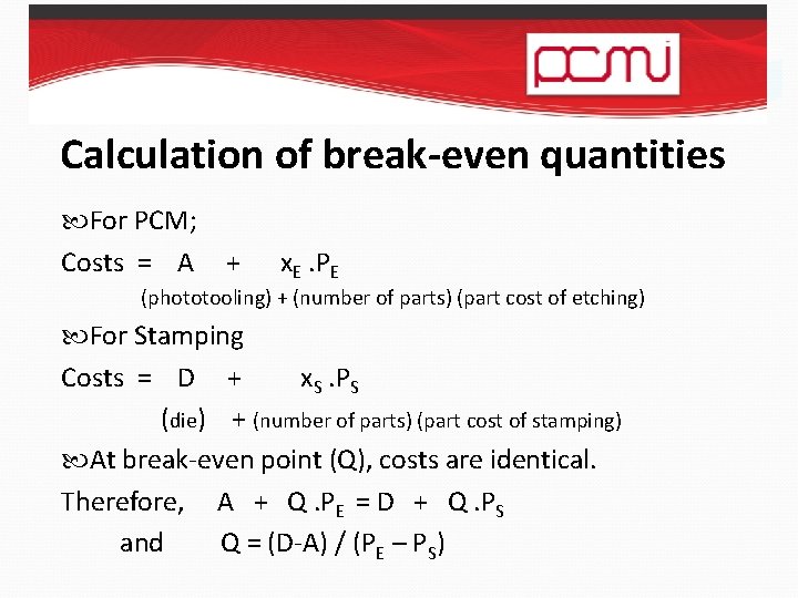
Calculation of break-even quantities For PCM; Costs = A + x. E. PE (phototooling) + (number of parts) (part cost of etching) For Stamping Costs = D + x. S. PS (die) + (number of parts) (part cost of stamping) At break-even point (Q), costs are identical. Therefore, A + Q. PE = D + Q. PS and Q = (D-A) / (PE – PS)

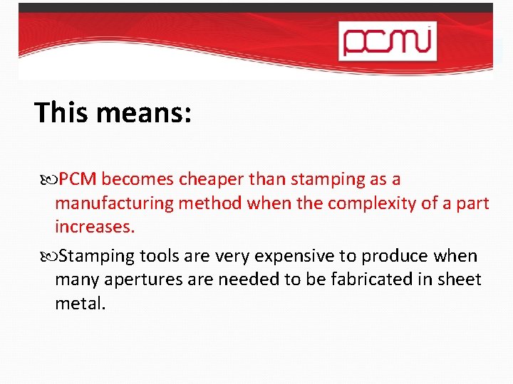
This means: PCM becomes cheaper than stamping as a manufacturing method when the complexity of a part increases. Stamping tools are very expensive to produce when many apertures are needed to be fabricated in sheet metal.

What happens when more rival processes are considered? § Consider the processes of § Wire-electrodischarge machining (WEDM) § Laser beam machining (LBM) § Photochemical machining (PCM) § Photoelectroforming (PEF) So which is the cheapest manufacturing technique? The answer is summarised in the next two slides.

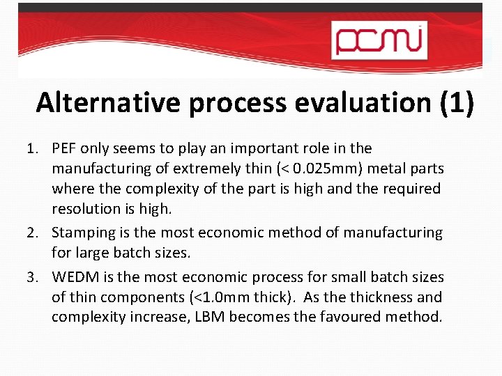
Alternative process evaluation (1) 1. PEF only seems to play an important role in the manufacturing of extremely thin (< 0. 025 mm) metal parts where the complexity of the part is high and the required resolution is high. 2. Stamping is the most economic method of manufacturing for large batch sizes. 3. WEDM is the most economic process for small batch sizes of thin components (<1. 0 mm thick). As the thickness and complexity increase, LBM becomes the favoured method.

Alternative process evaluation (2) 4. For medium batch production, LBM and PCM rival each other for cost-effectiveness. The favoured method depends on part complexity. For instance, for a 0. 5 mm thick part, the more complex the component the more the economics favour PCM. This is understandable as all apertures are machined simultaneously in PCM. However, in LBM each aperture or edge is machined individually so that complex parts increase machining time and cost. As thickness increases, LBM increases its cost-effectiveness and as thickness decreases, PCM predominates as the etching time is reduced.

Conclusions PCM is a rapid manufacturing process for fabricating a very wide range of high resolution parts in thin materials. The parts are often flat but can be “folded” to produce 3 -D boxes and enclosures. The range of materials machined by PCM includes all metals but the more difficult-to-machine polymers, ceramics and glasses can also be machined by some specialist PCM companies. The PCM process is economically competitive in comparison with other manufacturing processes and is usually the cheapest process when part complexity is high.

References for further study (1) • • Allen D. M. , 2016, Photochemical Machining and Photoelectroforming, ISBN 978 -1 -5262 -0188 -1 Allen D. M. , Gillbanks P. J. and Palmer, A. J. , 1989, The selection of an appropriate method to manufacture thin sheet metal components based on technical and financial considerations, Proceedings ISEM-9, Nagoya, Japan Publications of the PCMI (obtainable from PCMI via www. pcmi. org) including: Visser A. and Weissinger D. , 1993, Spray Etching of Stainless Steel, University of Bremen Production Engineering Dept. , PCMI Publication #4000

References for further study (2) • • • Kapp-Schwörer D, Meier K and Gantner C, 2004, Liquid resists for photochemical machining, PCMI Journal, 92, 29 -42. Korsse H, 1992, Experience with ferric chloride regeneration, PCMI Journal, 49, 11 -14. Mc. Gregor D R, 1998, Aqueous resist development considerations for fine feature resist image formation, PCMI Journal, 71, 9 -13. West D, 2009, Trends in process control and automation strategies in the photochemical machining industry, PCMI Journal, 113, 6 -10. Wilson W, 2009, Dry film imaging considerations for photochemical machining, PCMI Journal, 112, 20 -21. Wilson W, 2013, How to optimise dry film adhesion to various metal surfaces, PCMI Journal, 122, 166 -180.

Acknowledgements Prof. David Allen and PCMI wish to acknowledge the collaboration and help given by the members of the Photo Chemical Machining Institute in compiling this presentation. Further details of the PCMI and its members can be found at www. pcmi. org. April 2016