The First 3 D Multiproject Run for HEP
- Slides: 21

The First 3 D Multiproject Run for HEP Ray Yarema On behalf of 3 DIC Consortium September 23, 2009 Paris, France Topical Workshop on Experiments for Particle Physics

Introduction/Background • In late 2008 a large number of international laboratories and universities with interest in High Energy Physics formed a consortium for the development of 3 D integrated circuits. The first joint effort was to organize a 3 D multi-project run utilizing wafers from the Chartered 0. 13 um CMOS process and 3 D assembly by Tezzaron. This talk will present an overview of that multi-project wafer run. Topical Workshop on Experiments for Particle Physics 2

Consortium for 3 D IC Design • Consortium presently comprised of 15 members from 5 countries – – – University at Bergamo University at Pavia University at Perugia INFN Bologna INFN at Pisa INFN at Rome CPPM, Marseilles IPHC, Strasbourg IRFU Saclay LAL, Orsay LPNHE, Paris CMP, Grenoble – University of Bonn – AGH University of Science &Technology, Poland – Fermilab, Batavia • Others contributing to first MPW – BNL, Brookhaven – LBNL, Berkeley Topical Workshop on Experiments for Particle Physics 3

Consortium • To join – NDA with Tezzaron – LOI to Fermilab asking to participate in MPW run – Only cost is for MPW space • Members receive from Tezzaron – Cadence PDK for Chartered 0. 13 um – Calibre DRC/LVS/PEX(XRC) deck for Chartered 0. 13 um CMOS with correct process options – Calibre DRC deck for Tezzaron 3 D design rules • Cu-cu bond interface • Via formation – Information for fabrication of 2 D and 3 D I/O pads – ARM Artisan library (separate NDA) • Full-layout views – Also available but not used (separate cost for each) • Benefits – Sharing of design blocks • • Bergamo/Pavia Strasbourg LBNL FNAL CPPM FNAL Strasbourg Standardized bond interface, scribe line templates, alignment targets – Sharing of special software/libraries • Fill program by CMP • Assura DRC/LVS/RCX deck by FNAL • Mixed signal library with separate substrate and ground connections by FNAL – Design reviews • First check of each design done by FNAL – Cost reduction through MPW sharing – Sharing of results – to come soon • Webpage – http: //3 dic. fnal. gov • Micro. Magic 3 DMax (alternative to Virtuoso) • Magma (working on 3 D LVS) Topical Workshop on Experiments for Particle Physics 4

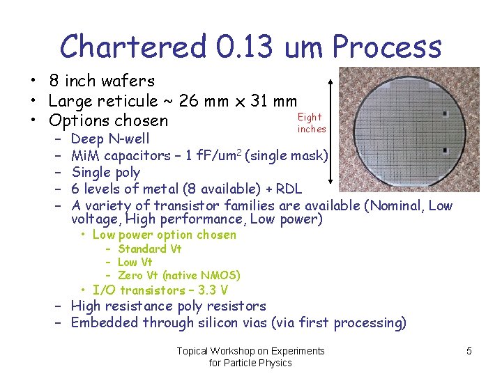
Chartered 0. 13 um Process • 8 inch wafers • Large reticule ~ 26 mm x 31 mm Eight • Options chosen inches – – – Deep N-well Mi. M capacitors – 1 f. F/um 2 (single mask) Single poly 6 levels of metal (8 available) + RDL A variety of transistor families are available (Nominal, Low voltage, High performance, Low power) • Low power option chosen – Standard Vt – Low Vt – Zero Vt (native NMOS) • I/O transistors – 3. 3 V – High resistance poly resistors – Embedded through silicon vias (via first processing) Topical Workshop on Experiments for Particle Physics 5

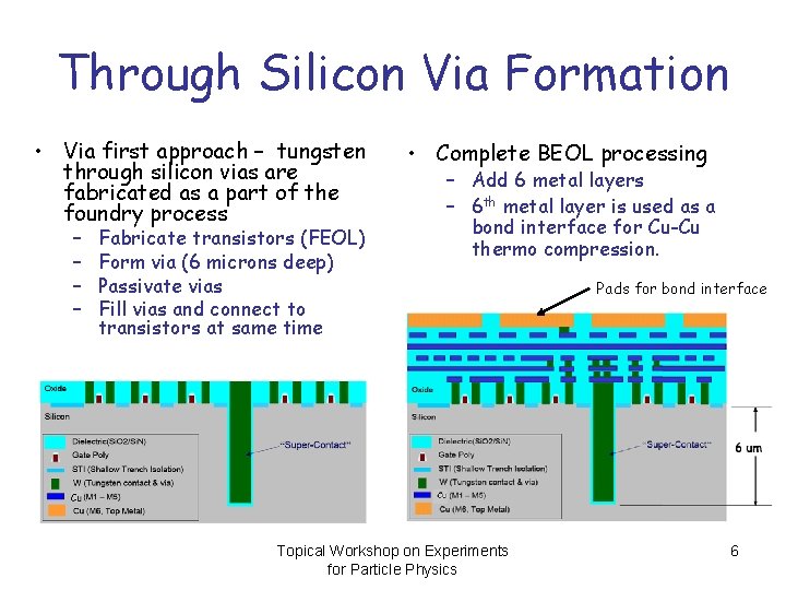
Through Silicon Via Formation • Via first approach – tungsten through silicon vias are fabricated as a part of the foundry process – – Fabricate transistors (FEOL) Form via (6 microns deep) Passivate vias Fill vias and connect to transistors at same time • Complete BEOL processing – Add 6 metal layers – 6 th metal layer is used as a bond interface for Cu-Cu thermo compression. Topical Workshop on Experiments for Particle Physics Pads for bond interface 6

Bond Interface • The bond interface is critical for good yield. – Makes electrical and mechanical connections from one wafer to the other wafer. – Bond interface must be strong enough to withstand subsequent thinning process. – There must be very uniform M 6 density across all designs and streets in the MPW run reticule. – Standard bond interface provided for all designers. • Mass of bond interface is insignificant – M 6 is ~. 8 microns thick, coverage ~ 35% – Two M 6 layers with 35% coverage gives 1. 6 um of Cu resulting in Xo=0. 0056% Topical Workshop on Experiments for Particle Physics 7

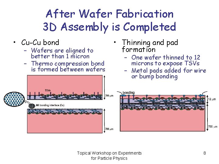
After Wafer Fabrication 3 D Assembly is Completed • Cu-Cu bond – Wafers are aligned to better than 1 micron – Thermo compression bond is formed between wafers • Thinning and pad formation – One wafer thinned to 12 microns to expose TSVs – Metal pads added for wire or bump bonding Topical Workshop on Experiments for Particle Physics 8

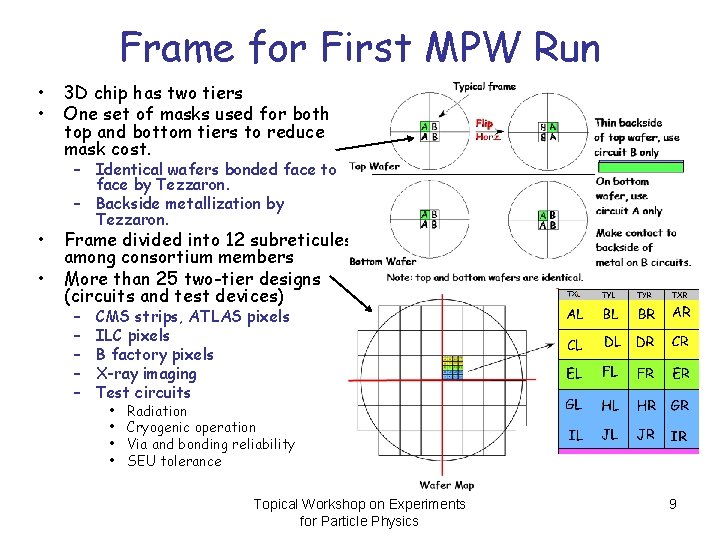
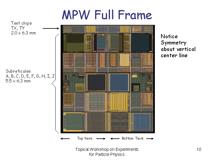
Frame for First MPW Run • • 3 D chip has two tiers One set of masks used for both top and bottom tiers to reduce mask cost. – Identical wafers bonded face to face by Tezzaron. – Backside metallization by Tezzaron. Frame divided into 12 subreticules among consortium members More than 25 two-tier designs (circuits and test devices) – – – CMS strips, ATLAS pixels ILC pixels B factory pixels X-ray imaging Test circuits • • Radiation Cryogenic operation Via and bonding reliability SEU tolerance Topical Workshop on Experiments for Particle Physics 9

Test chips: TX, TY 2. 0 x 6. 3 mm MPW Full Frame Notice Symmetry about vertical center line Subreticules: A, B, C, D, E, F, G, H, I, J 5. 5 x 6. 3 mm Top tiers Bottom Tiers Topical Workshop on Experiments for Particle Physics 10

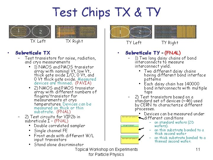
Test Chips TX & TY 1 2 TX Left • Subreticule TX – – 1 TX Right 2 TY Left • TY Right Subreticule TY – (FNAL) Test transistors for noise, radiation, – 1) Two long daisy chains of bond and cryo measurements interconnects to measure interconnect yield. • 1) NMOS and PMOS transistor array with nominal Vt, low Vt, • Two different daisy chains thick gate oxide I/O, 0 Vt, and having different bond interface 0 Vt thick gate oxide. Measured patterns devices are thinned. (PAVIA) • Each daisy chain has 140000 • 2) NMOS and PMOS transistor bond interconnects with multiple array with different numbers of taps fingers/transistor for – 2) Test transistors based on a measurements at cryo standard set of devices (~46) used temperatures. Devices can be by CERN to characterize different measured on thick or thin processes. substrate. (FNAL) • Devices can be measured under 2) Test circuits for VIP 2 b in different conditions subreticule I – (FNAL) – on standard wafers (2 D wafers). • Double correlated sampler – on thin substrate bonded to a • Single channel FE thick second wafer • Front ends with different W/L – on thick substrate bonded to a input transistors thinned second wafer. • Stand alone discriminator Topical Workshop on Experiments 11 for Particle Physics

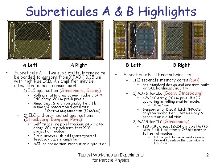
Subreticules A & B Highlights 1 1 2 A Left • A Right Subreticule A – Two subcircuits, intended to be bonded to sensors from XFAB ( 0. 35 um with high Res EPI). An amplifier may be integrated in each sensor pixel – 1) ILC application (Strasbourg, Saclay) • • – Rolling shutter, low power tracker, 34 X 240 array, 20 um pitch pixels Amp, Disc. & latch on analog tier, 1 bit memory& readout on digital tier – 2 B Left • • – • • Self triggering pixel tracker, 245 x 245 array, 20 um pitch with fast X-Y projection readout 2 sub arrays with different types of feedback caps in amplifier ASD on analog tier, readout on digital tier one standard design and one with built -in SEL hardness circuitry 2) MAPS for ILC (Scaly, Strasbourg) • 42 x 240 array, 20 um pixel MAPS operating in rolling shutter mode, • 2) ILC and bio-medical applications • B Right Subreticule B – Three subcircuits – 1) 2 separate memory cores (CMP) R. O. time=integration time (80 ns/row) (Strasbourg, Bergamo, Pavia) 3 – – 80 ns/row – Future goal: to use separate sensor tier and to reduce the pixel size to 12 x 12 um. Sensor, amp, Disc & latch (NMOS only) on analog tier. 1 bit memory & readout on digital tier 3) MAPS for ILC (Strasbourg) • 128 x 192 array, 12 x 24 um pixel MAPS with 5 bit time stamp, 2 nd hit marker, full serial readout Topical Workshop on Experiments for Particle Physics 12

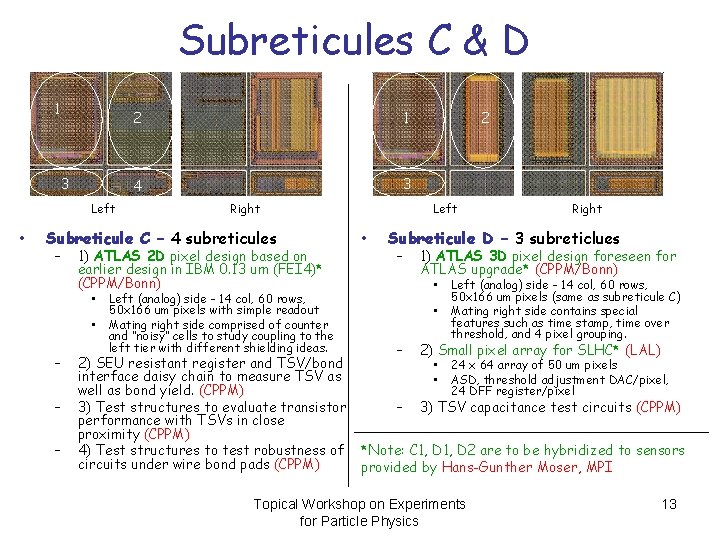
Subreticules C & D 1 3 Left • 2 1 4 3 Right Subreticule C – 4 subreticules – 1) ATLAS 2 D pixel design based on earlier design in IBM 0. 13 um (FEI 4)* (CPPM/Bonn) • • – – – Left (analog) side - 14 col, 60 rows, 50 x 166 um pixels with simple readout Mating right side comprised of counter and “noisy” cells to study coupling to the left tier with different shielding ideas. 2) SEU resistant register and TSV/bond interface daisy chain to measure TSV as well as bond yield. (CPPM) 3) Test structures to evaluate transistor performance with TSVs in close proximity (CPPM) 4) Test structures to test robustness of circuits under wire bond pads (CPPM) 2 Left • Right Subreticule D – 3 subreticlues – 1) ATLAS 3 D pixel design foreseen for ATLAS upgrade* (CPPM/Bonn) • • Left (analog) side - 14 col, 60 rows, 50 x 166 um pixels (same as subreticule C) Mating right side contains special features such as time stamp, time over threshold, and 4 pixel grouping. – 2) Small pixel array for SLHC* (LAL) – 3) TSV capacitance test circuits (CPPM) • • 24 x 64 array of 50 um pixels ASD, threshold adjustment DAC/pixel, 24 DFF register/pixel *Note: C 1, D 2 are to be hybridized to sensors provided by Hans-Gunther Moser, MPI Topical Workshop on Experiments for Particle Physics 13

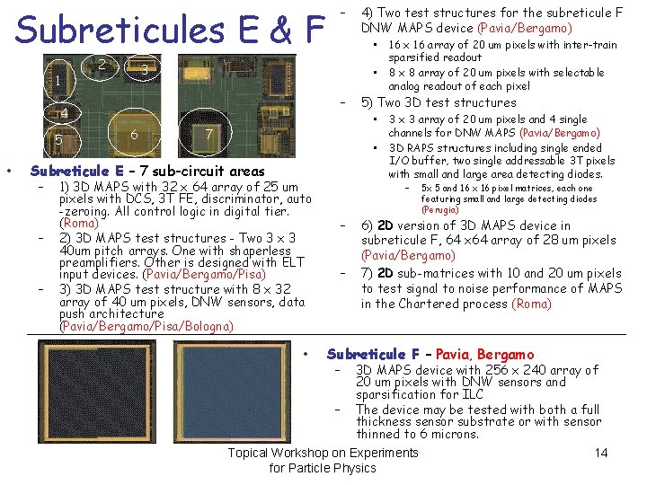
Subreticules E & F 1 2 • – • 6 7 – – 1) 3 D MAPS with 32 x 64 array of 25 um pixels with DCS, 3 T FE, discriminator, auto -zeroing. All control logic in digital tier. (Roma) 2) 3 D MAPS test structures - Two 3 x 3 40 um pitch arrays. One with shaperless preamplifiers. Other is designed with ELT input devices. (Pavia/Bergamo/Pisa) 3) 3 D MAPS test structure with 8 x 32 array of 40 um pixels, DNW sensors, data push architecture (Pavia/Bergamo/Pisa/Bologna) • 16 x 16 array of 20 um pixels with inter-train sparsified readout 8 x 8 array of 20 um pixels with selectable analog readout of each pixel 5) Two 3 D test structures • • Subreticule E – 7 sub-circuit areas – 4) Two test structures for the subreticule F DNW MAPS device (Pavia/Bergamo) • 3 4 5 – 3 x 3 array of 20 um pixels and 4 single channels for DNW MAPS (Pavia/Bergamo) 3 D RAPS structures including single ended I/O buffer, two single addressable 3 T pixels with small and large area detecting diodes. – – – 5 x 5 and 16 x 16 pixel matrices, each one featuring small and large detecting diodes (Perugia) 6) 2 D version of 3 D MAPS device in subreticule F, 64 x 64 array of 28 um pixels (Pavia/Bergamo) 7) 2 D sub-matrices with 10 and 20 um pixels to test signal to noise performance of MAPS in the Chartered process (Roma) Subreticule F – Pavia, Bergamo – – 3 D MAPS device with 256 x 240 array of 20 um pixels with DNW sensors and sparsification for ILC The device may be tested with both a full thickness sensor substrate or with sensor thinned to 6 microns. Topical Workshop on Experiments for Particle Physics 14

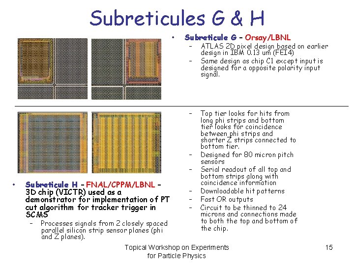
Subreticules G & H • Subreticule G – Orsay/LBNL – – – • Subreticule H – FNAL/CPPM/LBNL – 3 D chip (VICTR) used as a demonstrator for implementation of PT cut algorithm for tracker trigger in SCMS – Processes signals from 2 closely spaced parallel silicon strip sensor planes (phi and Z planes). – – – ATLAS 2 D pixel design based on earlier design in IBM 0. 13 um (FEI 4) Same design as chip C 1 except input is designed for a opposite polarity input signal. Top tier looks for hits from long phi strips and bottom tier looks for coincidence between phi strips and shorter Z strips connected to bottom tier. Designed for 80 micron pitch sensors Serial readout of all top and bottom strips along with coincidence information Downloadable hit patterns Fast OR outputs Circuit to be thinned to 24 microns and connections made to both the top and bottom of the chip. Topical Workshop on Experiments for Particle Physics 15

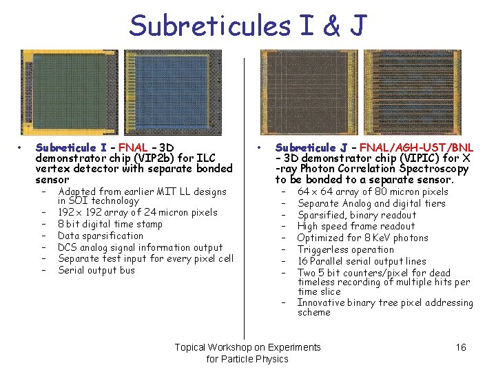
Subreticules I & J • Subreticule I – FNAL – 3 D demonstrator chip (VIP 2 b) for ILC vertex detector with separate bonded sensor – – – – Adapted from earlier MIT LL designs in SOI technology 192 x 192 array of 24 micron pixels 8 bit digital time stamp Data sparsification DCS analog signal information output Separate test input for every pixel cell Serial output bus • Subreticule J – FNAL/AGH-UST/BNL – 3 D demonstrator chip (VIPIC) for X -ray Photon Correlation Spectroscopy to be bonded to a separate sensor. – – – – – 64 x 64 array of 80 micron pixels Separate Analog and digital tiers Sparsified, binary readout High speed frame readout Optimized for 8 Ke. V photons Triggerless operation 16 Parallel serial output lines Two 5 bit counters/pixel for dead timeless recording of multiple hits per time slice Innovative binary tree pixel addressing scheme Topical Workshop on Experiments for Particle Physics 16

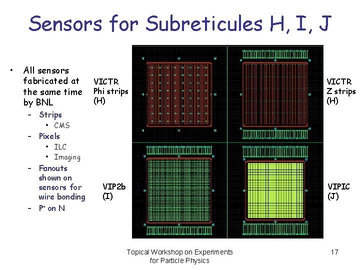
Sensors for Subreticules H, I, J • All sensors fabricated at the same time by BNL VICTR Phi strips (H) VICTR Z strips (H) – Strips • CMS – Pixels • ILC • Imaging – Fanouts shown on sensors for wire bonding – P+ on N VIP 2 b (I) VIPIC (J) Topical Workshop on Experiments for Particle Physics 17

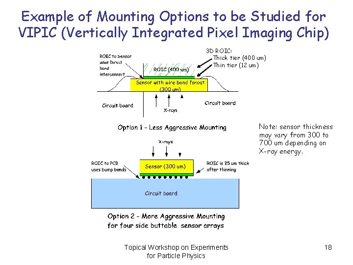
Example of Mounting Options to be Studied for VIPIC (Vertically Integrated Pixel Imaging Chip) 3 D ROIC: Thick tier (400 um) Thin tier (12 um) Note: sensor thickness may vary from 300 to 700 um depending on X-ray energy. Topical Workshop on Experiments for Particle Physics 18

Timeline • First Designers meeting held Dec 11, 2008 • Subsequent meeting in February, March, and May 2009 • All designs initially submitted by mid May – Continuous checking of designs by Tezzaron and Fermilab identified numerous problems • • • Inconsistent layer map tables between designs Different DRC violations found with Assura, Calibre, and Magma Non uniform bond interface across all subreticules Via size confusion related to 2 top metals Non mirroring of design in frame Adding of high resistance poly option Computer system crashes at Tezzaron Problems with Micro. Magic and Magma Satisfying/answering all of Chartered’s questions – Items changed during review process • Dummy fill program • Via density rule • Newer DRC versions uploaded. • Masks started for 31 wafers • 8 weeks for wafer fabrication. • 4 weeks for 3 D assembly Topical Workshop on Experiments for Particle Physics 19

The Future • In some sense this HEP MPW run was a learning experience for both Tezzaron and the HEP community. • Tezzaron is currently planning for a DARPA run due to close December 15 – 5 tiers, 2 -3 tiers of memory (1 Gb/tier + 2 tiers of digital) – ~25 customers – Oversold by 400 % • New institutions have expressed an interest in joining the 3 DIC consortium. • In part due to our HEP run, both CMP and MOSIS have expressed interest in providing some sort of 3 D IC services. • Consortia hopes to have 1 -2 runs in 2010. Topical Workshop on Experiments for Particle Physics 20

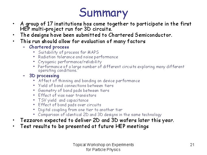
Summary • • • A group of 17 institutions has come together to participate in the first HEP multi-project run for 3 D circuits. The designs have been submitted to Chartered Semiconductor. This run should allow for evaluation of many factors – Chartered process • • Suitability of process for MAPS Radiation tolerance and noise performance Cryogenic performance/reliability Performance of a large number of different circuits exploring many different operating conditions. – 3 D processing • • • Affect of thinning and bonding on device performance Yield of bond connections between tiers Geometry of bond pads between tiers Effect of vias near transistors TSV yield and capacitance Effect of bond pads over circuits Digital coupling from one tier to another tier Comparison of identical 2 D and 3 D designs in the same technology Tezzaron expected to deliver 2 D and 3 D wafers later this year. Test results to be presented at future HEP meetings Topical Workshop on Experiments for Particle Physics 21