The design of fast analog channels for the

- Slides: 1

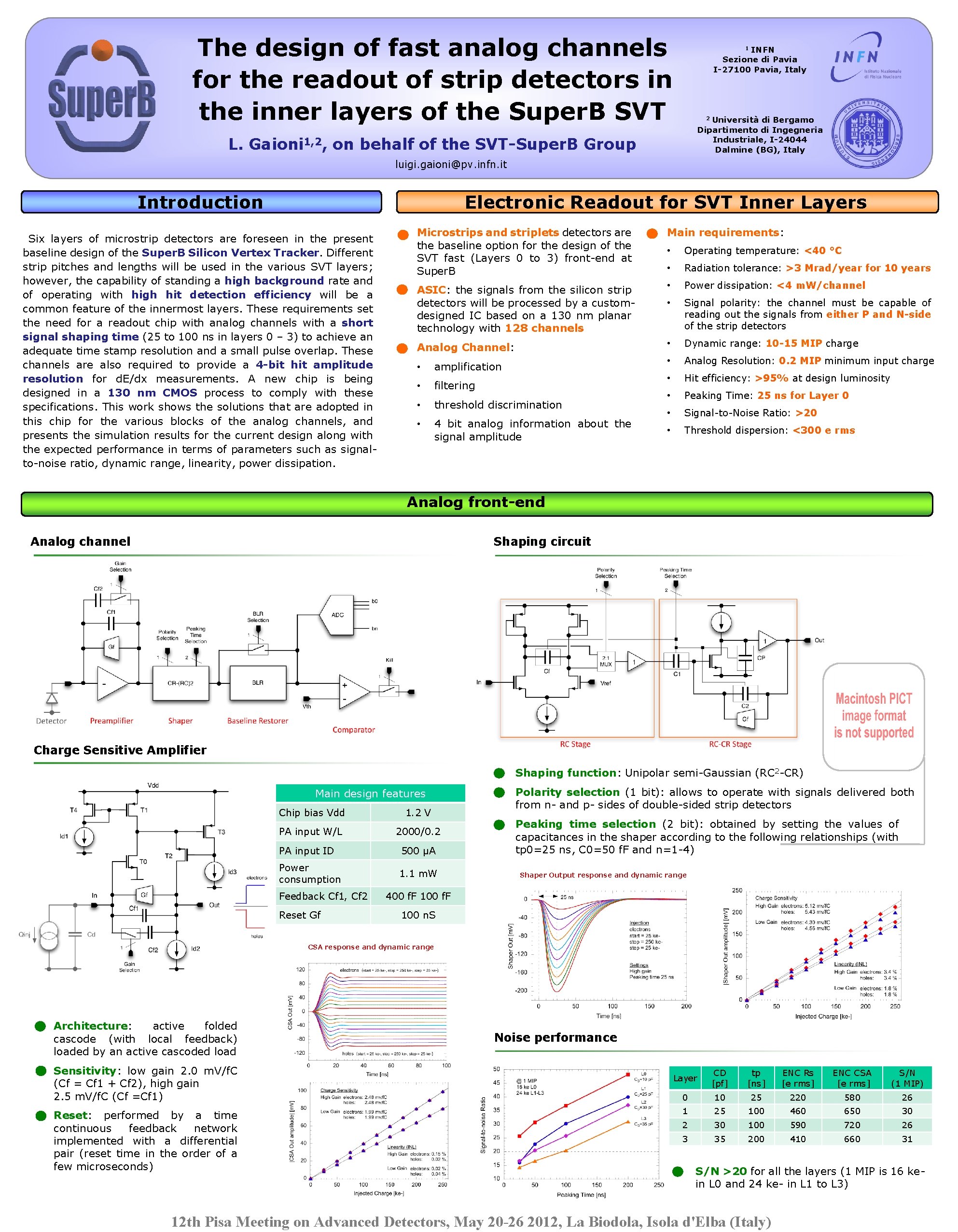
The design of fast analog channels for the readout of strip detectors in the inner layers of the Super. B SVT INFN Sezione di Pavia I-27100 Pavia, Italy 1 Università di Bergamo Dipartimento di Ingegneria Industriale, I-24044 Dalmine (BG), Italy 2 L. Gaioni 1, 2, on behalf of the SVT-Super. B Group luigi. gaioni@pv. infn. it Introduction Electronic Readout for SVT Inner Layers Six layers of microstrip detectors are foreseen in the present baseline design of the Super. B Silicon Vertex Tracker. Different strip pitches and lengths will be used in the various SVT layers; however, the capability of standing a high background rate and of operating with high hit detection efficiency will be a common feature of the innermost layers. These requirements set the need for a readout chip with analog channels with a short signal shaping time (25 to 100 ns in layers 0 – 3) to achieve an adequate time stamp resolution and a small pulse overlap. These channels are also required to provide a 4 -bit hit amplitude resolution for d. E/dx measurements. A new chip is being designed in a 130 nm CMOS process to comply with these specifications. This work shows the solutions that are adopted in this chip for the various blocks of the analog channels, and presents the simulation results for the current design along with the expected performance in terms of parameters such as signalto-noise ratio, dynamic range, linearity, power dissipation. • • • Microstrips and striplets detectors are the baseline option for the design of the SVT fast (Layers 0 to 3) front-end at Super. B • Main requirements: • Operating temperature: <40 °C • Radiation tolerance: >3 Mrad/year for 10 years ASIC: the signals from the silicon strip detectors will be processed by a customdesigned IC based on a 130 nm planar technology with 128 channels • Power dissipation: <4 m. W/channel • Signal polarity: the channel must be capable of reading out the signals from either P and N-side of the strip detectors Analog Channel: • Dynamic range: 10 -15 MIP charge • amplification • Analog Resolution: 0. 2 MIP minimum input charge • filtering • Hit efficiency: >95% at design luminosity • threshold discrimination • Peaking Time: 25 ns for Layer 0 • 4 bit analog information about the signal amplitude • Signal-to-Noise Ratio: >20 • Threshold dispersion: <300 e rms Analog front-end Analog channel Shaping circuit Charge Sensitive Amplifier Main design features Chip bias Vdd 1. 2 V PA input W/L 2000/0. 2 PA input ID 500 µA Power consumption 1. 1 m. W Feedback Cf 1, Cf 2 Reset Gf • Shaping function: Unipolar semi-Gaussian (RC 2 -CR) • Polarity selection (1 bit): allows to operate with signals delivered both from n- and p- sides of double-sided strip detectors • Peaking time selection (2 bit): obtained by setting the values of capacitances in the shaper according to the following relationships (with tp 0=25 ns, C 0=50 f. F and n=1 -4) Shaper Output response and dynamic range 400 f. F 100 n. S CSA response and dynamic range • Architecture: active folded cascode (with local feedback) loaded by an active cascoded load • Sensitivity: low gain 2. 0 m. V/f. C (Cf = Cf 1 + Cf 2), high gain 2. 5 m. V/f. C (Cf =Cf 1) • Reset: performed by a time continuous feedback network implemented with a differential pair (reset time in the order of a few microseconds) Noise performance Layer CD [pf] tp [ns] ENC Rs [e rms] ENC CSA [e rms] S/N (1 MIP) 0 10 25 220 580 26 1 25 100 460 650 30 2 30 100 590 720 26 3 35 200 410 660 31 • S/N >20 for all the layers (1 MIP is 16 kein L 0 and 24 ke- in L 1 to L 3) 12 th Pisa Meeting on Advanced Detectors, May 20 -26 2012, La Biodola, Isola d'Elba (Italy)