THE DESIGN AGAINST RADIATION EFFECTS DARE DESIGN PLATFORM


- Slides: 18

THE DESIGN AGAINST RADIATION EFFECTS (DARE) DESIGN PLATFORM FOR TSMC 65 NM PROCESS. M. KAKOULIN, S. REDANT, G. THYS, S. VERHAEGEN, G. FRANCISCATTO, B. CHEHAB, G. POLLISSARD, L. BERTI AMICSA, 2018 CONFIDENTIAL

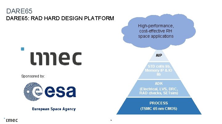
DARE 65: RAD HARD DESIGN PLATFORM High-performance, cost-effective RH space applications AIP STD cells lib, Memory IP & IO lib Sponsored by: ADK (Electrical, LVS, DRC, RAD checks, SETsim) PROCESS (TSMC 65 nm CMOS) 2 CONFIDENTIAL

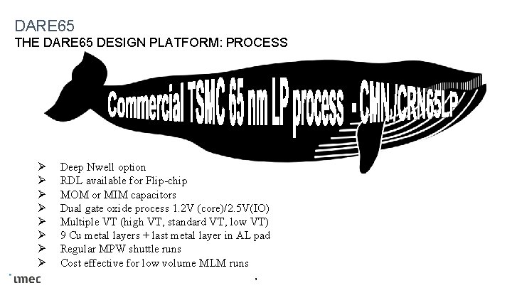
DARE 65 THE DARE 65 DESIGN PLATFORM: PROCESS Ø Ø Ø Ø Deep Nwell option RDL available for Flip-chip MOM or MIM capacitors Dual gate oxide process 1. 2 V (core)/2. 5 V(IO) Multiple VT (high VT, standard VT, low VT) 9 Cu metal layers + last metal layer in AL pad Regular MPW shuttle runs Cost effective for low volume MLM runs 3 CONFIDENTIAL

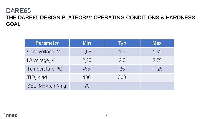
DARE 65 THE DARE 65 DESIGN PLATFORM: OPERATING CONDITIONS & HARDNESS GOAL Parameter Min Typ Max Core voltage, V 1, 08 1, 2 1, 32 IO voltage, V 2, 25 2, 75 Temperature, 0 C -55 25 +125 TID, krad 100 300 SEL, Me. V. cm 2/mg 70 4 CONFIDENTIAL

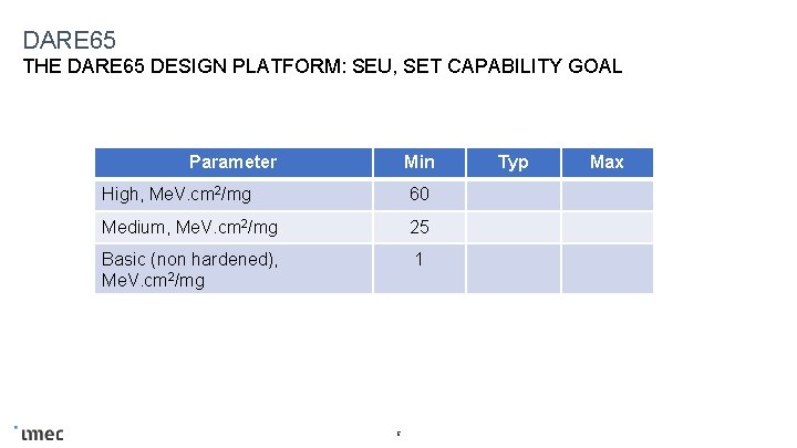
DARE 65 THE DARE 65 DESIGN PLATFORM: SEU, SET CAPABILITY GOAL Parameter Min High, Me. V. cm 2/mg 60 Medium, Me. V. cm 2/mg 25 Basic (non hardened), Me. V. cm 2/mg 1 5 Typ Max CONFIDENTIAL

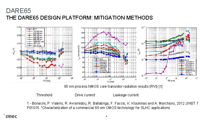
DARE 65 THE DARE 65 DESIGN PLATFORM: MITIGATION METHODS 65 nm process NMOS core transistor radiation results (RVt) [1] Threshold Drive current Leakage current 1 - Bonacini, P. Valerio, R. Avramidou, R. Ballabriga, F. Faccio, K. Kloukinas and A. Marchioro, 2012 JINST 7 P 01015. “Characterization of a commercial 65 nm CMOS technology for SLHC applications 6 CONFIDENTIAL

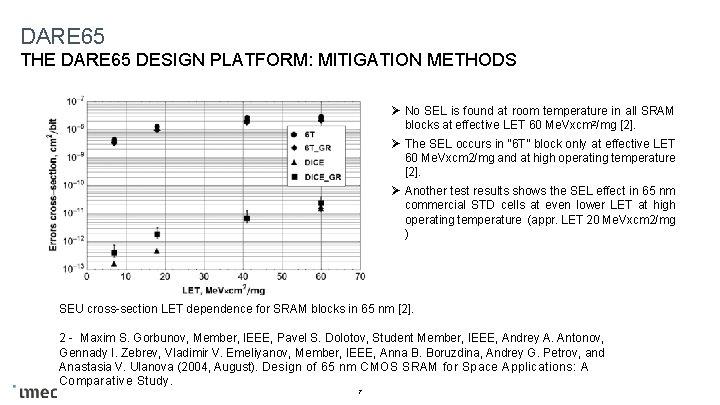
DARE 65 THE DARE 65 DESIGN PLATFORM: MITIGATION METHODS Ø No SEL is found at room temperature in all SRAM blocks at effective LET 60 Me. Vxcm 2/mg [2]. Ø The SEL occurs in “ 6 T” block only at effective LET 60 Me. Vxcm 2/mg and at high operating temperature [2]. Ø Another test results shows the SEL effect in 65 nm commercial STD cells at even lower LET at high operating temperature (appr. LET 20 Me. Vxcm 2/mg ) SEU cross-section LET dependence for SRAM blocks in 65 nm [2]. 2 - Maxim S. Gorbunov, Member, IEEE, Pavel S. Dolotov, Student Member, IEEE, Andrey A. Antonov, Gennady I. Zebrev, Vladimir V. Emeliyanov, Member, IEEE, Anna B. Boruzdina, Andrey G. Petrov, and Anastasia V. Ulanova (2004, August). Design of 65 nm CMOS SRAM for Space Applications: A Comparative Study. 7 CONFIDENTIAL

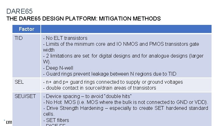
DARE 65 THE DARE 65 DESIGN PLATFORM: MITIGATION METHODS Factor TID - No ELT transistors - Limits of the minimum core and IO NMOS and PMOS transistors gate width - 2 limitations are set: for digital designs and for analogue designs (larger W). - Deep N-well - Guard rings prevent leakage between N regions due to TID SEL - n+ and p+ guard rings connected to supply or ground voltages - double contact in source/drain areas of transistors SEU/SET - Device spacing – to avoid “double hits” - No Hot MOS (i. e. MOS where the bulk is not connected to GND or VDD). - Drive Strength Hardening – especially to create SET hardened standard cells. - SET filters 8 CONFIDENTIAL

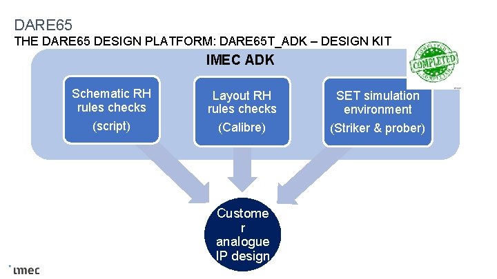
DARE 65 THE DARE 65 DESIGN PLATFORM: DARE 65 T_ADK – DESIGN KIT IMEC ADK Schematic RH rules checks (script) Layout RH rules checks (Calibre) SET simulation environment (Striker & prober) Custome r analogue IP design 9 CONFIDENTIAL

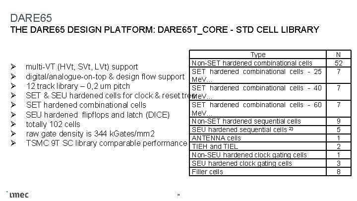
DARE 65 THE DARE 65 DESIGN PLATFORM: DARE 65 T_CORE - STD CELL LIBRARY Ø Ø Ø Ø Ø Type Non-SET hardened combinational cells multi-VT (HVt, SVt, LVt) support SET hardened combinational cells - 25 digital/analogue-on-top & design flow support Me. V. . . 12 track library – 0, 2 um pitch SET hardened combinational cells - 40 SET & SEU hardened cells for clock & reset tree. Me. V. . . SET hardened combinational cells - 60 SET hardened combinational cells Me. V. . . SEU hardened flipflops and latch (DICE) Non-SET hardened sequential cells totally 102 cells SEU hardened sequential cells 2) raw gate density is 344 k. Gates/mm 2 ANTENNA cells TSMC 9 T SC library comparable performance TIEH and TIEL Non-SEU hardened clock gating cells Filler cells 10 N 52 7 7 7 9 5 1 2 1 3 8 CONFIDENTIAL

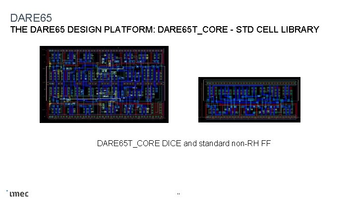
DARE 65 THE DARE 65 DESIGN PLATFORM: DARE 65 T_CORE - STD CELL LIBRARY DARE 65 T_CORE DICE and standard non-RH FF 11 CONFIDENTIAL

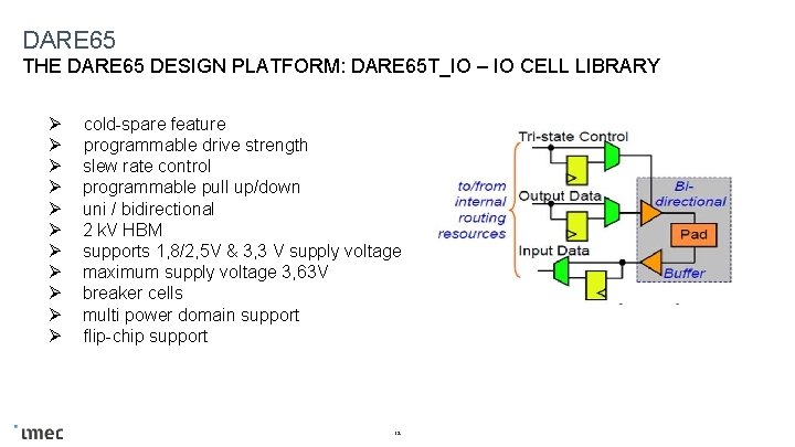
DARE 65 THE DARE 65 DESIGN PLATFORM: DARE 65 T_IO – IO CELL LIBRARY Ø Ø Ø cold-spare feature programmable drive strength slew rate control programmable pull up/down uni / bidirectional 2 k. V HBM supports 1, 8/2, 5 V & 3, 3 V supply voltage maximum supply voltage 3, 63 V breaker cells multi power domain support flip-chip support 12 CONFIDENTIAL

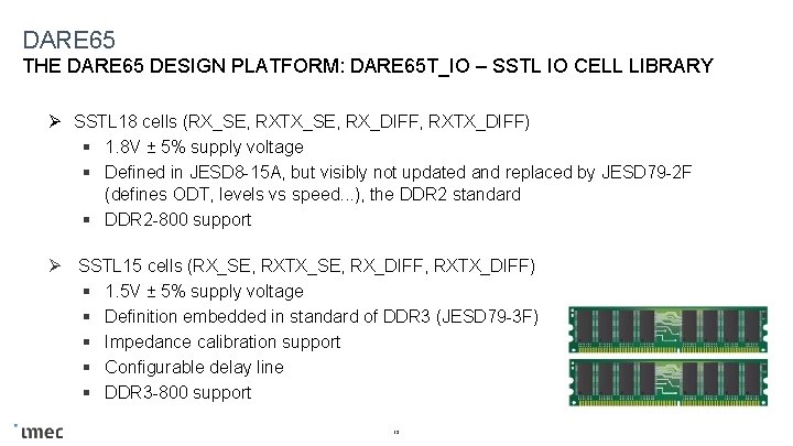
DARE 65 THE DARE 65 DESIGN PLATFORM: DARE 65 T_IO – SSTL IO CELL LIBRARY Ø SSTL 18 cells (RX_SE, RXTX_SE, RX_DIFF, RXTX_DIFF) § 1. 8 V ± 5% supply voltage § Defined in JESD 8 -15 A, but visibly not updated and replaced by JESD 79 -2 F (defines ODT, levels vs speed. . . ), the DDR 2 standard § DDR 2 -800 support Ø SSTL 15 cells (RX_SE, RXTX_SE, RX_DIFF, RXTX_DIFF) § 1. 5 V ± 5% supply voltage § Definition embedded in standard of DDR 3 (JESD 79 -3 F) § Impedance calibration support § Configurable delay line § DDR 3 -800 support 13 CONFIDENTIAL

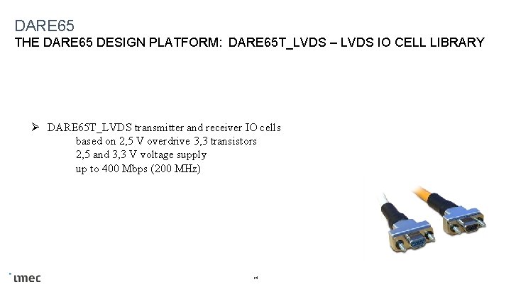
DARE 65 THE DARE 65 DESIGN PLATFORM: DARE 65 T_LVDS – LVDS IO CELL LIBRARY Ø DARE 65 T_LVDS transmitter and receiver IO cells based on 2, 5 V overdrive 3, 3 transistors 2, 5 and 3, 3 V voltage supply up to 400 Mbps (200 MHz) 14 CONFIDENTIAL

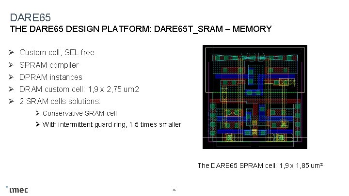
DARE 65 THE DARE 65 DESIGN PLATFORM: DARE 65 T_SRAM – MEMORY Ø Custom cell, SEL free Ø SPRAM compiler Ø DPRAM instances Ø DRAM custom cell: 1, 9 x 2, 75 um 2 Ø 2 SRAM cells solutions: Ø Conservative SRAM cell Ø With intermittent guard ring, 1, 5 times smaller The DARE 65 SPRAM cell: 1, 9 x 1, 85 um 2 15 CONFIDENTIAL

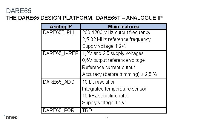
DARE 65 THE DARE 65 DESIGN PLATFORM: DARE 65 T – ANALOGUE IP Analog IP DARE 65 T_PLL Main features 200 -1200 MHz output frequency 2, 5 -32 MHz reference frequency Supply voltage 1, 2 V. DARE 65_IVREF 1, 2 V and 2, 5 supply voltages 0, 6 V output reference voltage Reference current output Accuracy (before trimming) ± 2, 5 % DARE 65_ADC 10 bit resolution Integrated temperature sensor 10 k. Hz sampling rate. Supply voltage 1, 2 V. DARE 65_POR TBD 16 CONFIDENTIAL

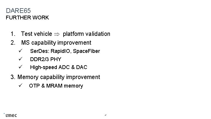
DARE 65 FURTHER WORK 1. Test vehicle platform validation 2. MS capability improvement ü ü ü Ser. Des: Rapid. IO, Space. Fiber DDR 2/3 PHY High-speed ADC & DAC 3. Memory capability improvement ü OTP & MRAM memory 17 CONFIDENTIAL

CONFIDENTIAL