The BTe V Tracking Systems f David Christian
The BTe. V Tracking Systems f David Christian Fermilab January 11, 2001
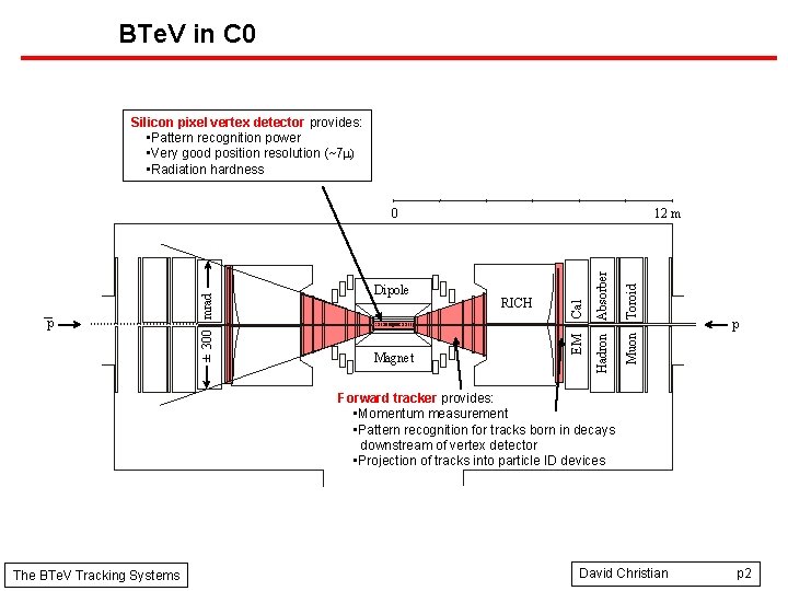
BTe. V in C 0 Silicon pixel vertex detector provides: • Pattern recognition power • Very good position resolution (~7 m) • Radiation hardness Absorber Toroid Hadron Muon Magnet RICH Cal Dipole 12 m EM p ± 300 mrad 0 p Forward tracker provides: • Momentum measurement • Pattern recognition for tracks born in decays downstream of vertex detector • Projection of tracks into particle ID devices The BTe. V Tracking Systems David Christian p 2
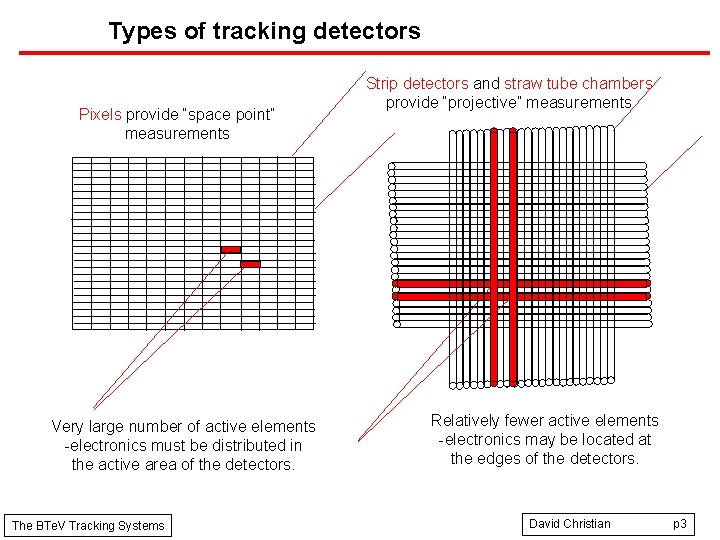
Types of tracking detectors Pixels provide “space point” measurements Very large number of active elements -electronics must be distributed in the active area of the detectors. The BTe. V Tracking Systems Strip detectors and straw tube chambers provide “projective” measurements Relatively fewer active elements -electronics may be located at the edges of the detectors. David Christian p 3
Forward Tracker Forward tracker consists of: • Straw chambers • Cost effective solution for large area coverage • High segmentation (baseline=4 mm diameter straws) • Can “clamshell” around beam pipe without a heavy frame in the active area • Robust: a broken wire does not kill an entire plane • Short drift times (single crossing memory time) • Good precision good momentum, mass resolution • Silicon strip detectors • 100 mm pitch low occupancy, even near the beam pipe • More radiation hard than straws The BTe. V Tracking Systems David Christian p 4
Silicon Strip Detectors (SSD’s) • Near the beam pipe, the density of tracks is too high for straws to handle (occupancy, radiation damage) • Central 24 cm x 24 cm will be covered with SSD’s (central hole for the beam pipe) • 6 stations per spectrometer arm; 3 views per station 100 mm pitch; 108000 readout channels • “CMS style” single sided p-on-n sensors • Planar geometry – easier than barrel The BTe. V Tracking Systems David Christian p 5
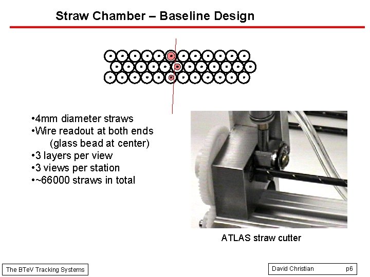
Straw Chamber – Baseline Design • 4 mm diameter straws • Wire readout at both ends (glass bead at center) • 3 layers per view • 3 views per station • ~66000 straws in total ATLAS straw cutter The BTe. V Tracking Systems David Christian p 6
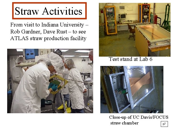
Straw Activities From visit to Indiana University – Rob Gardner, Dave Rust – to see ATLAS straw production facility Test stand at Lab 6 Close-up of UC Davis/FOCUS straw chamber p 7
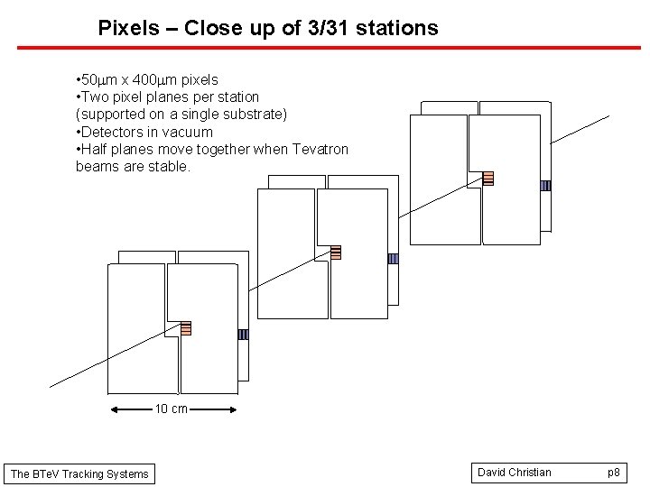
Pixels – Close up of 3/31 stations • 50 mm x 400 mm pixels • Two pixel planes per station (supported on a single substrate) • Detectors in vacuum • Half planes move together when Tevatron beams are stable. 10 cm The BTe. V Tracking Systems David Christian p 8
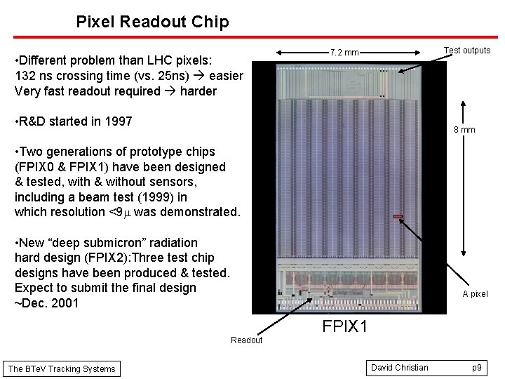
Pixel Readout Chip • Different problem than LHC pixels: 132 ns crossing time (vs. 25 ns) easier Very fast readout required harder Test outputs 7. 2 mm • R&D started in 1997 8 mm • Two generations of prototype chips (FPIX 0 & FPIX 1) have been designed & tested, with & without sensors, including a beam test (1999) in which resolution <9 m was demonstrated. • New “deep submicron” radiation hard design (FPIX 2): Three test chip designs have been produced & tested. Expect to submit the final design ~Dec. 2001 A pixel FPIX 1 Readout The BTe. V Tracking Systems David Christian p 9
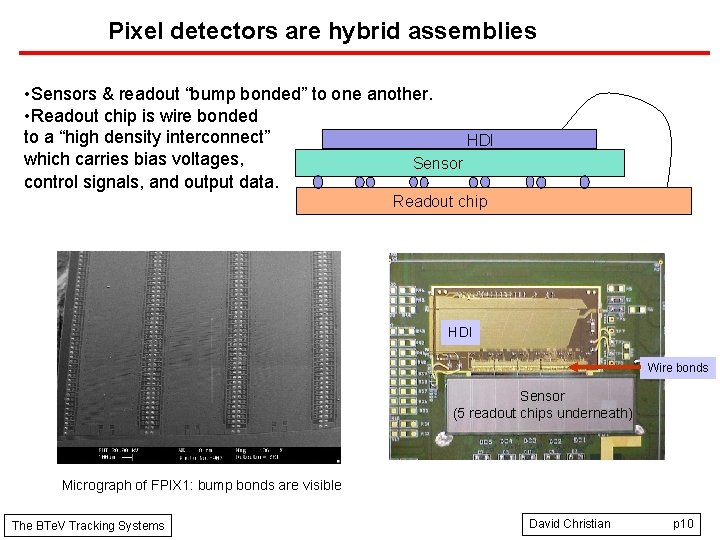
Pixel detectors are hybrid assemblies • Sensors & readout “bump bonded” to one another. • Readout chip is wire bonded to a “high density interconnect” HDI which carries bias voltages, Sensor control signals, and output data. Readout chip HDI Wire bonds Sensor (5 readout chips underneath) Micrograph of FPIX 1: bump bonds are visible The BTe. V Tracking Systems David Christian p 10
Tracking Systems R&D Status • Pixel detector component-level R&D is quite advanced – focus now shifting to system design, including low mass support & cooling structure, vacuum vessel, & motion control. (Fermilab, Syracuse, Iowa) • Straw detector R&D activities have begun. – Lab 6 test stand working. – Prototype detector (96 straws) to be built in 2001. (Fermilab, S. M. U. , U. C. Davis, Indiana U. ) • Silicon Strip Detector R&D is being led by University groups (Milano, Tennessee, Colorado). – Readout chip development starting in Milano. – Balance of effort is concentrating on system design and construction techniques. – Expect to benefit greatly from sensor development done for LHC and from Fermilab experience (CDF & D 0 - Si. Det). The BTe. V Tracking Systems David Christian p 11
- Slides: 11