The BTe V pixel vertex detector Luigi Moroni

The BTe. V pixel vertex detector Luigi Moroni INFN-Milano Beauty 99 at Bled

Outline Would like to summarize • the principles which inspired the project • the status of the R&D • the results from the tests of the prototypes and to conclude with • our program for the near future

Principles at the base of the project We believe that • any reliable way to do b-physics in the forward regions of p-pbar colliders requires very fine pitch pixel detectors This is even more true if • we want to select events with secondary vertices already at the trigger 1 st Level

In fact • BTe. V wants to reconstruct the tracks and the primary vertex in order to elaborate a trigger decision based on track impact parameters already at the 1 st Level NB: we do not have any Level 0 trigger! This means that • independently of any other condition, every single -pbar event has to be readout without deadtime and • to improve the resolution, analog readout is needed. p

Now the question is • are we able to built such a detector? • a real challenge! The good news is that • we are very close to demonstrate that we know how to build the pixel detector for BTe. V and • in a short time, we will produce a proof of principle.

31 triplets of pixel planes across the collision region, 3. 2 cm apart Pixel geometry in each triplet 50 x 400 µm 2

The challenge • High radiation tolerance • about the same as for LHC experiments, 1014 particles / year • Very fast analog readout • considering a pixel size of 50 400 µm 2 and a 8 7. 2 mm 2 pixel sensor located 6 mm from the beam, we expect an average of 1. 25 pixel hits per BCO @ L = 2 1032 cm-2 sec-1 • this is an average rate: we should be able to handle the fluctuations too!

Pixel readout chip development for BTe. V The BTe. V R&D program started about 2 years ago at FNAL • The effort envisions the design and the production of a sequence of prototypes, FPIXi, each devoted to a specific goal • 2 prototypes have been already fabricated • FPIX 0 and FPIX 1
 • to establish a front-end design")
• FPIX 0 (delivered on Sept 97) • to establish a front-end design appropriate for use at the TEVATRON collider • optimized for 132 nsec crossing time • able to tolerate large sensor leakage current • deadtimeless operation • FPIX 1 (delivered on Dec 98) • to establish a readout architecture capable to meet the BTe. V requirements • high speed zero suppression • should readout 2 pixels per BCO at least

Both prototypes were designed • to mate the ATLAS n+/n sensors, 50 400 µm 2 • to be compatible with the Honeywell 0. 5 µm CMOS-SOI Rad Hard process. We are now considering the alternative offered by the new deep submicron CMOS processes • intrinsic resistance to the radiation • more flexibility in the design
 First stage feedback element in box: “Synthetic")
FPIX 0 Front end* (HP 0. 8µ) First stage feedback element in box: “Synthetic Resistor” = transistor which acts as a resistor for small signals and as a constant current source (discharging the feedback capacitor) for large signals (or large leakage current). Threshold Cinj Vin + - 50 W to grnd to peak sensor n p Chip boundary Pixel detector unit cell boundary -V(detector bias) Vout Analog test output Vout / Vin = 1. 3 * See Blanquart, et al. NIMA 395, p 313 (1997)

FPIX 0 bonded to ATLAS ST-1 Amplifier output is directly connected to wire bond pads for 4 pixel cells: 3 bonded 1 unbonded Indium bump bonded by Boeing
 produces")
FPIX 0 absolute calibration • Terbium fluorescence K peak (44. 5 Ke. V) produces 12, 300 e -h pairs in Silicon 30. 2 input electrons per m. V peak output signal
> = 87 e<Noise(bonded)> = 95")
Measurements: 64 bonded and 64 unbonded pixel cells <Noise(unbonded)> = 87 e<Noise(bonded)> = 95 e- If all added noise is attributed to input capacitance (sensor+bump) SPICE ==> Cin is approx. 180 f. F

FPIX Amplifier is designed to be insensitive to sensor leakage current. Test of sensitivity to leakage current: Measurements made by injecting charge into three cells of an FPIX 0 which is bump bonded to an ATLAS (Seiko) ST-1 sensor. The sensor was biased at -75 V. The n-side guard ring was allowed to float, so that all current measured by the “HV” power supply goes through the bonded pixels… we assume that the current is shared equally by the 704 bonded pixels. The next two pages show the response of a standard gain amplifier and of a high gain amplifier to a 200 m. V (8000 e-) injection pulse under the following conditions: 1) Sensor covered; bias current ~ 23 n. A (0. 03 n. A/pixel). 2) Sensor uncovered, lit by desk lamp; bias current ~ 15 m. A (~ 20 n. A/pixel). 3) Sensor uncovered, brighter light; bias current ~ 74 m. A (~ 105 n. A/pixel).
 I_fb = 7 n. A Leakage current ~ 0")
Standard gain cell (7, 0) I_fb = 7 n. A Leakage current ~ 0 DC offset is due to the effect of light on the FPIX 0 itself, not sensor leakage current. Leakage current ~20 n. A/pixel High gain cell (9, 0) I_fb = 7 n. A Leakage current ~ 0 Standard gain cell (11, 0) (Not bonded to sensor) I_fb = 7 n. A Leakage current ~ 0 Leakage current ~20 n. A/pixel
 I_fb = 7 n. A Leakage current ~ 0")
Standard gain cell (7, 0) I_fb = 7 n. A Leakage current ~ 0 Leakage current ~20 n. A/pixel High gain cell (9, 0) I_fb = 7 n. A Leakage current ~ 0 Leakage current ~20 n. A/pixel FPIX 0 Insensitivity to leakage current: High gain cell can be adjusted so that rise time & amplitude with ~20 n. A/pixel of leakage current match the rise time & amplitude with no leakage current. High gain cell (9, 0) I_fb = 0. 5 n. A Leakage current ~ 0 Leakage current ~20 n. A/pixel

FPIX 0 amplifiers work even with 100 n. A/pixel of leakage current. Standard gain cell (7, 0) I_fb = 7 n. A Leakage current ~ 0 Leakage current ~20 n. A/pixel Leakage current ~ 100 n. A/pixel (note 50 m. V/div vertical scale) High gain cell (9, 0) I_fb = 7 n. A Leakage current ~ 0 Leakage current ~20 n. A/pixel Leakage current ~ 100 n. A/pixel (note 100 m. V/div vertical scale)

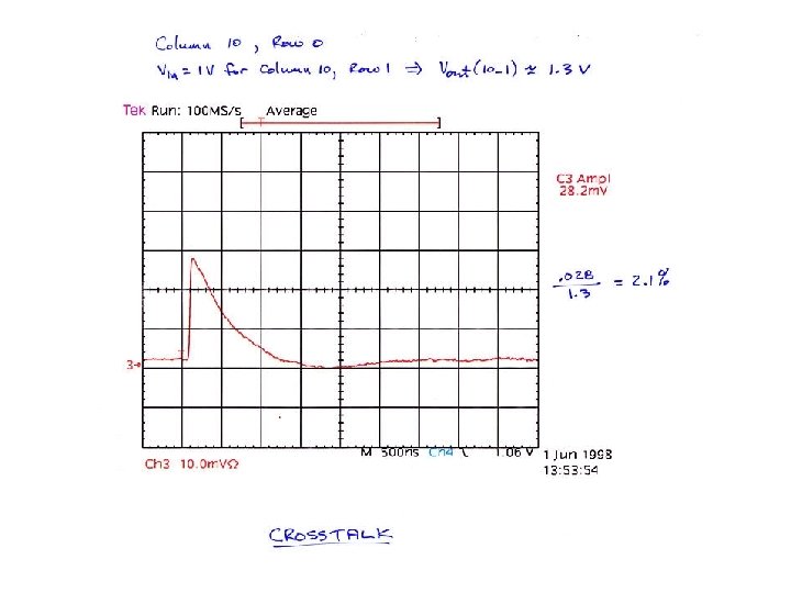
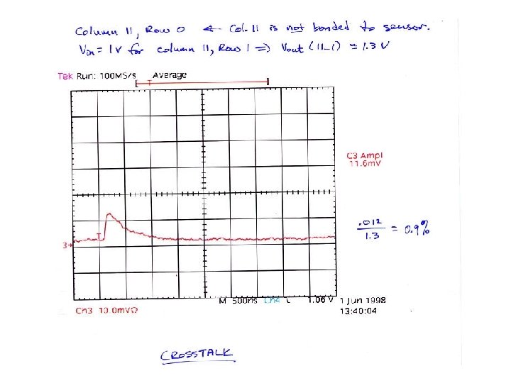
FPIX 0 test results: summary • <Noise> 95 e- rms ( 90 e- unbonded ) • Threshold dispersion 500 e- ( 400 e- unbonded) • Insensitive to sensor leakage current up to 100 n. A/pixel • These 3 figures can be further improved by going at higher gain, i. e. Cf = 10 f. F instead of Cf = 20 f. F Cf(FPIX 1) = 10 f. F • Crosstalk between adjacent pixels 2% at most FPIX 0 works well!

FPIX 1: features • Contains an optimized version of FPIX 0 front-end • New fully digital readout architecture (column based) • Very fast while preserving analog information • Each cell includes a 2 -bit FADC • Our simulations indicate that only few bits are necessary for a good resolution • Will check this point in the test beam this summer

Use of Pulse Height Information Expected behavior of the resolution as a function of the # of bits used for AD conversion (Artuso & Wang) • 50 m wide pixels • Y layer shows effect of 1. 6 T dipole field
 9 candidate front end designs (20 copies of")
Pre-FPIX 1 (HP 0. 5 m) 9 candidate front end designs (20 copies of each) FPIX 1 will use 2 stage amp, DC coupled to discriminator (like FPIX 0). AC coupling would require more area in the pixel unit cell without yielding a significant advantage.

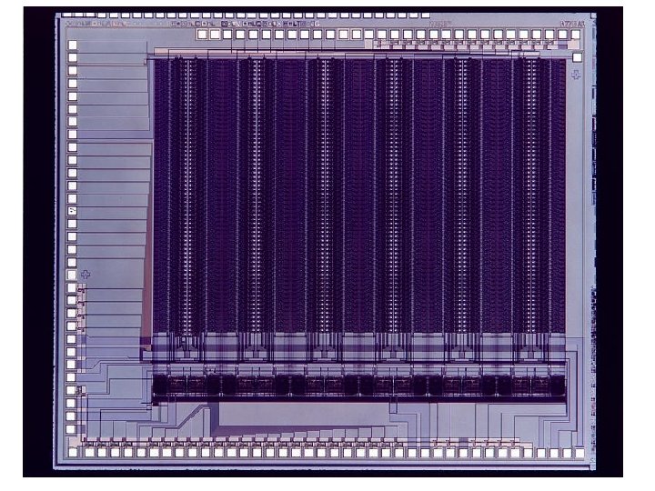
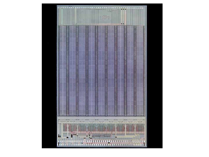
FPIX 1 Floor Plan One column is read out under external control Wire bond pads Direct amplifier & discriminator outputs from top row of pixels Pixel Unit Cell Sensor pixels cover light blue area: 160 rows x 18 columns 50 x 400 m (8 mm x 7. 2 mm) Normal readout to EOC & off chip (17 columns) Power distribution Double row of bond pads End of column logic and busses Chip control logic

FPIX 1: Pixel Unit Cell Thresholds Readout clock Vdda ADC Token in Command Interpreter Sensor Pixel kill Threshold Test 00 - idle 01 - reset 10 - output 11 - look for data 4 pairs of command lines RFast. OR HFast. OR ADC Bus Controller Row Address Token out

FPIX 1: preliminary test results • Front-end and readout work as designed • Dynamic range of the preamplifier 32 Ke • <Noise> 50 e- rms ( 90 e- in FPIX 0) • Threshold dispersion 240 e- ( 400 e- in FPIX 0) • High speed token passing: >5 GHz skip frequency 26. 5 MHz readout clock can be safely used an average of more than 3 pixels per BCO (132 nsec) can be readout

FPIX 1: present status The results from the preliminary tests of FPIX 1 are really encouraging Now, they are waiting for a confirmation in the beam Bump bonded detectors with FPIX 1 will be tested in the beam this summer
 a high thermal conductivity substrate with")
Mechanical and cooling issues Two basic approaches: 1) a high thermal conductivity substrate with heat sinks on the edges 2) a substrate with cooling channels embedded In both cases, the material budget is about 0. 8 % Rad Len

Conclusions The progress accomplished in only two years by the R&D activity on BTe. V pixel detectors is impressive • The experience of the other groups working in this field has been crucial We are very close to validate the key concepts and technologies and prepare TDR • At the end of this year we will have new results from the test beam Stay tuned & join us! BTe. V is an unique occasion to do b-physics in a very aggressive way in the next millennium


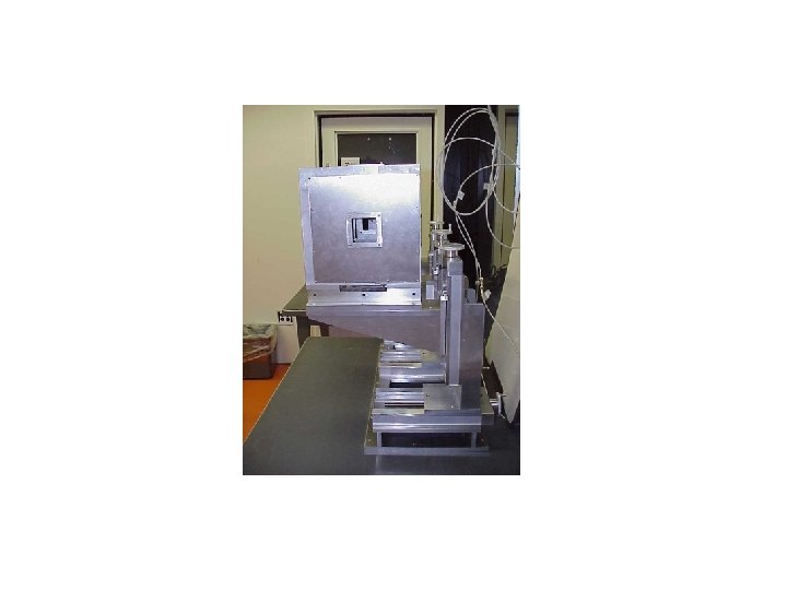
Beam Test Preparations: Mechanical support/enclosure for SSD telescope and pixel planes (copy of D 0 telescope used in the last fixed target run).
- Slides: 36