
The Associative Memory AM Bingo Dedicated device maximum
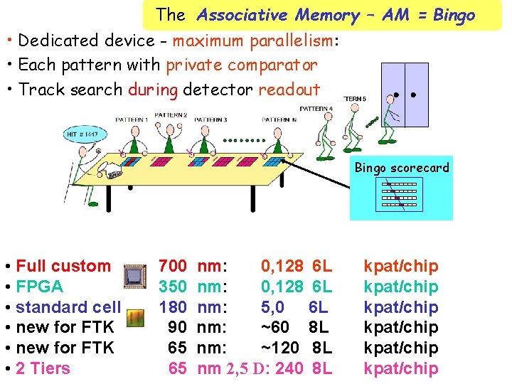
The Associative Memory – AM = Bingo • Dedicated device - maximum parallelism: • Each pattern with private comparator • Track search during detector readout Bingo scorecard • Full custom • FPGA • standard cell • new for FTK • 2 Tiers 700 350 180 90 65 65 nm: 0, 128 6 L nm: 5, 0 6 L nm: ~60 8 L nm: ~120 8 L nm 2, 5 D: 240 8 L kpat/chip kpat/chip
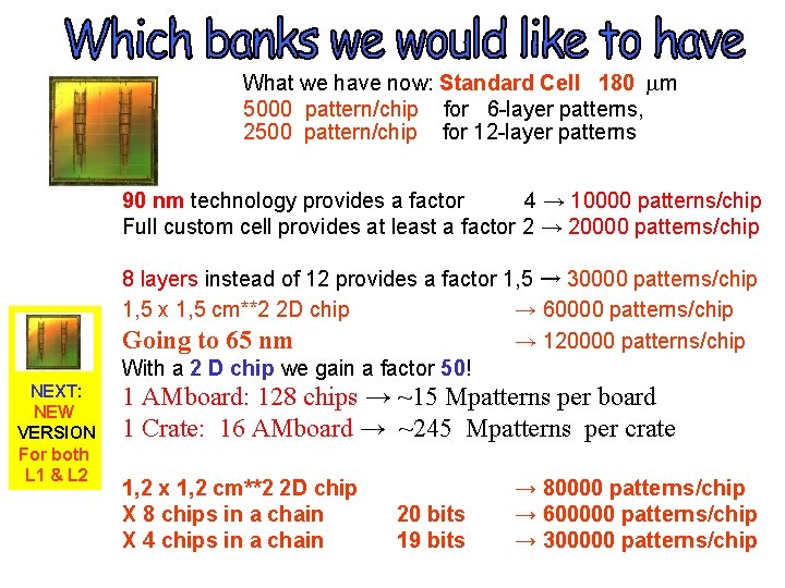
What we have now: Standard Cell 180 mm 5000 pattern/chip for 6 -layer patterns, 2500 pattern/chip for 12 -layer patterns 90 nm technology provides a factor 4 → 10000 patterns/chip Full custom cell provides at least a factor 2 → 20000 patterns/chip 8 layers instead of 12 provides a factor 1, 5 → 30000 patterns/chip 1, 5 x 1, 5 cm**2 2 D chip → 60000 patterns/chip Going to 65 nm → 120000 patterns/chip With a 2 D chip we gain a factor 50! NEXT: NEW VERSION For both L 1 & L 2 1 AMboard: 128 chips → ~15 Mpatterns per board 1 Crate: 16 AMboard → ~245 Mpatterns per crate 1, 2 x 1, 2 cm**2 2 D chip X 8 chips in a chain X 4 chips in a chain 20 bits 19 bits → 80000 patterns/chip → 600000 patterns/chip → 300000 patterns/chip
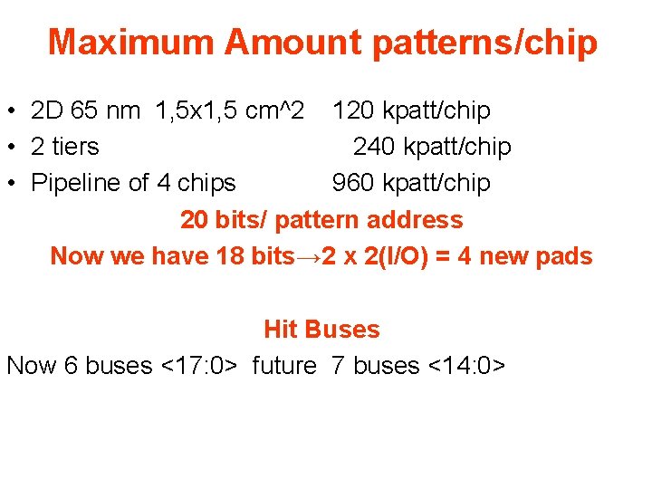
Maximum Amount patterns/chip • 2 D 65 nm 1, 5 x 1, 5 cm^2 120 kpatt/chip • 2 tiers 240 kpatt/chip • Pipeline of 4 chips 960 kpatt/chip 20 bits/ pattern address Now we have 18 bits→ 2 x 2(I/O) = 4 new pads Hit Buses Now 6 buses <17: 0> future 7 buses <14: 0>
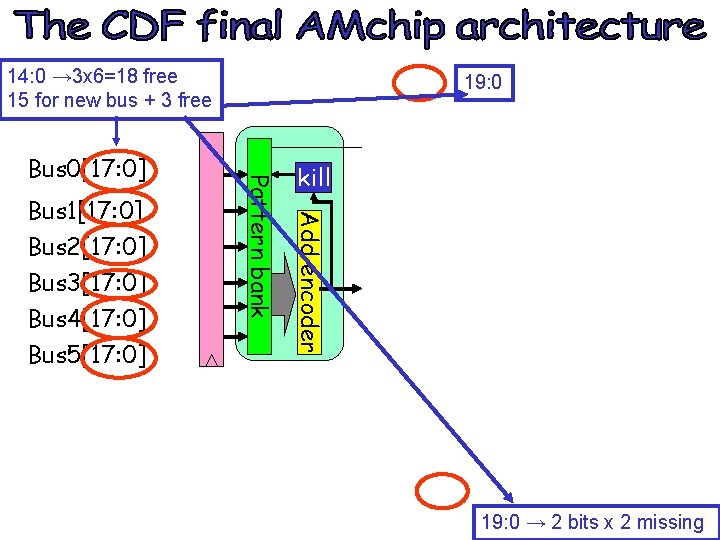
14: 0 → 3 x 6=18 free 15 for new bus + 3 free Bus 3[17: 0] Bus 4[17: 0] Bus 5[17: 0] kill Add encoder Bus 1[17: 0] Bus 2[17: 0] Pattern bank Bus 0[17: 0] 19: 0 → 2 bits x 2 missing
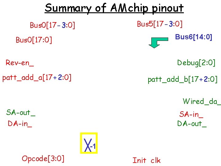
Summary of AMchip pinout Bus 5[17 -3: 0] Bus 0[17 -3: 0] Bus 6[14: 0] Bus 0[17: 0] Rev-en_ Debug[2: 0] patt_add_a[17+2: 0] patt_add_b[17+2: 0] Wired_da_ SA-out_ DA-in_ SA-in_ DA-out_ -1 Opcode[3: 0] Init clk
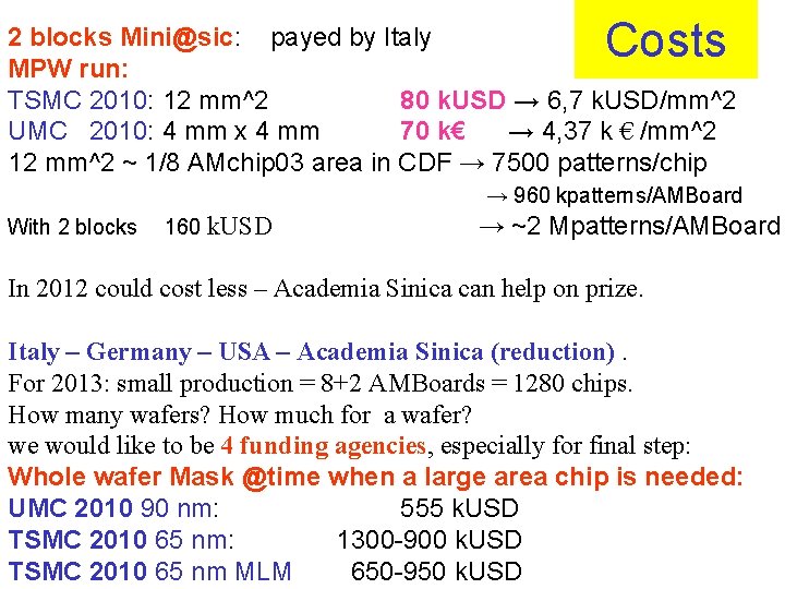
Costs 2 blocks Mini@sic: payed by Italy MPW run: TSMC 2010: 12 mm^2 80 k. USD → 6, 7 k. USD/mm^2 UMC 2010: 4 mm x 4 mm 70 k€ → 4, 37 k € /mm^2 12 mm^2 ~ 1/8 AMchip 03 area in CDF → 7500 patterns/chip → 960 kpatterns/AMBoard With 2 blocks 160 k. USD → ~2 Mpatterns/AMBoard In 2012 could cost less – Academia Sinica can help on prize. Italy – Germany – USA – Academia Sinica (reduction). For 2013: small production = 8+2 AMBoards = 1280 chips. How many wafers? How much for a wafer? we would like to be 4 funding agencies, especially for final step: Whole wafer Mask @time when a large area chip is needed: UMC 2010 90 nm: 555 k. USD TSMC 2010 65 nm: 1300 -900 k. USD TSMC 2010 65 nm MLM 650 -950 k. USD
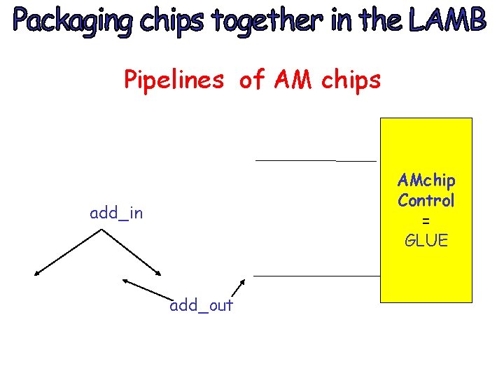
Pipelines of AM chips AMchip Control = GLUE add_in add_out
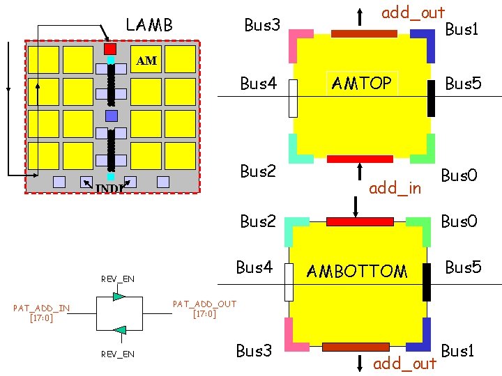
LAMB Bus 3 add_out Bus 1 AM Bus 4 Bus 2 INDI AMTOP add_in Bus 2 REV_EN Bus 4 Bus 5 Bus 0 AMBOTTOM Bus 5 PAT_ADD_OUT [17: 0] PAT_ADD_IN [17: 0] REV_EN Bus 3 add_out Bus 1
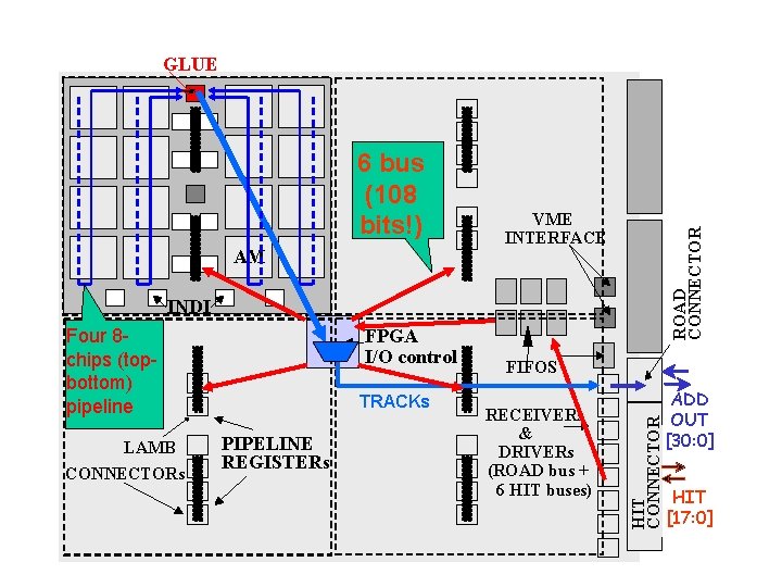
GLUE AM VME INTERFACE ROAD CONNECTOR 6 bus (108 bits!) INDI LAMB CONNECTORs FPGA I/O control TRACKs PIPELINE REGISTERs FIFOS RECEIVERs & DRIVERs (ROAD bus + 6 HIT buses) HIT CONNECTOR Four 8 chips (topbottom) pipeline ADD OUT [30: 0] HIT [17: 0]
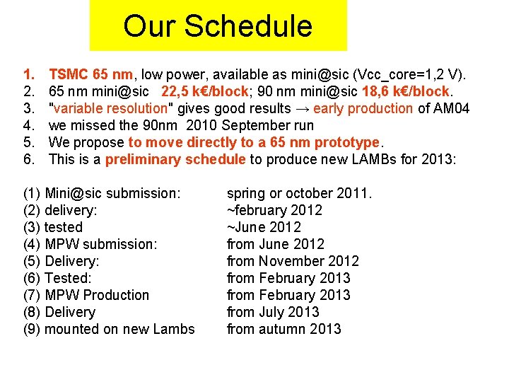
Our Schedule 1. 2. 3. 4. 5. 6. TSMC 65 nm, low power, available as mini@sic (Vcc_core=1, 2 V). 65 nm mini@sic 22, 5 k€/block; 90 nm mini@sic 18, 6 k€/block. "variable resolution" gives good results → early production of AM 04 we missed the 90 nm 2010 September run We propose to move directly to a 65 nm prototype. This is a preliminary schedule to produce new LAMBs for 2013: (1) Mini@sic submission: (2) delivery: (3) tested (4) MPW submission: (5) Delivery: (6) Tested: (7) MPW Production (8) Delivery (9) mounted on new Lambs spring or october 2011. ~february 2012 ~June 2012 from November 2012 from February 2013 from July 2013 from autumn 2013
- Slides: 10