The AM Chip SerDes IP Protocol Test Procedure
- Slides: 14

The AM Chip Ser/Des IP Protocol – Test Procedure Matteo Beretta 13 March 2013 FTK Workshop 1

Summary ● Parallel bus VS Serial link ● Ser/Des architecture ● Mini. Asic in/out architecture ● Ser/Des test features ● On board connection test ● Spread spectum modulator ● Mini. Asic data protocol 13 March 2013 FTK Workshop 2

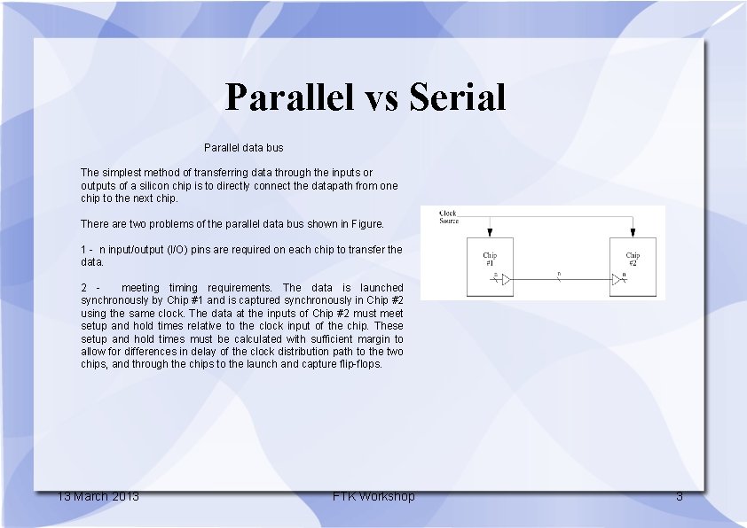
Parallel vs Serial Parallel data bus The simplest method of transferring data through the inputs or outputs of a silicon chip is to directly connect the datapath from one chip to the next chip. There are two problems of the parallel data bus shown in Figure. 1 - n input/output (I/O) pins are required on each chip to transfer the data. 2 meeting timing requirements. The data is launched synchronously by Chip #1 and is captured synchronously in Chip #2 using the same clock. The data at the inputs of Chip #2 must meet setup and hold times relative to the clock input of the chip. These setup and hold times must be calculated with sufficient margin to allow for differences in delay of the clock distribution path to the two chips, and through the chips to the launch and capture flip-flops. 13 March 2013 FTK Workshop 3

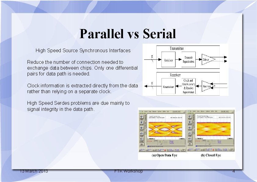
Parallel vs Serial High Speed Source Synchronous Interfaces Reduce the number of connection needed to exchange data between chips. Only one differential pairs for data path is needed. Clock information is extracted directly from the data rather than relying on a separate clock. High Speed Serdes problems are due mainly to signal integrity in the data path. 13 March 2013 FTK Workshop 4

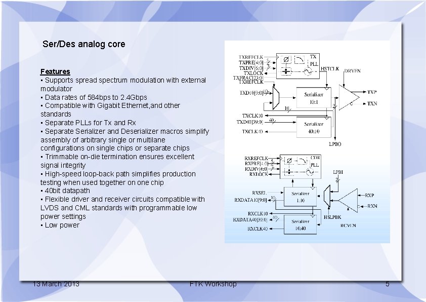
Ser/Des analog core Features • Supports spread spectrum modulation with external modulator • Data rates of 584 bps to 2. 4 Gbps • Compatible with Gigabit Ethernet, and other standards • Separate PLLs for Tx and Rx • Separate Serializer and Deserializer macros simplify assembly of arbitrary single or multilane configurations on single chips or separate chips • Trimmable on-die termination ensures excellent signal integrity • High-speed loop-back path simplifies production testing when used together on one chip • 40 bit datapath • Flexible driver and receiver circuits compatible with LVDS and CML standards with programmable low power settings • Low power 13 March 2013 FTK Workshop 5

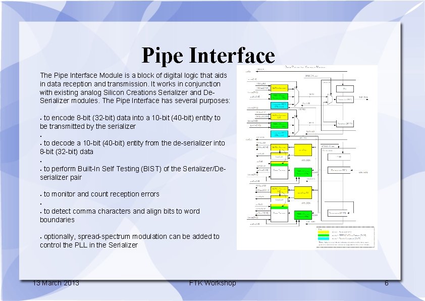
Pipe Interface The Pipe Interface Module is a block of digital logic that aids in data reception and transmission. It works in conjunction with existing analog Silicon Creations Serializer and De. Serializer modules. The Pipe Interface has several purposes: to encode 8 -bit (32 -bit) data into a 10 -bit (40 -bit) entity to be transmitted by the serializer ● ● to decode a 10 -bit (40 -bit) entity from the de-serializer into 8 -bit (32 -bit) data ● ● to perform Built-In Self Testing (BIST) of the Serializer/Deserializer pair ● ● to monitor and count reception errors ● to detect comma characters and align bits to word boundaries ● optionally, spread-spectrum modulation can be added to control the PLL in the Serializer ● 13 March 2013 FTK Workshop 6

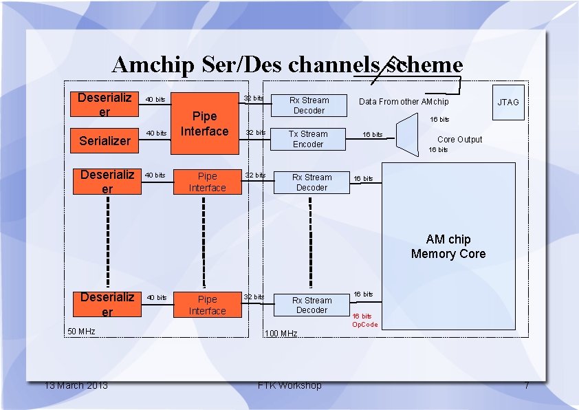
Amchip Ser/Des channels scheme Deserializ er Serializer Deserializ er 32 bits 40 bits Pipe Interface Rx Stream Decoder Data From other AMchip JTAG 16 bits 32 bits Tx Stream Encoder Rx Stream Decoder 16 bits Core Output 16 bits AM chip Memory Core Deserializ er 50 MHz 13 March 2013 40 bits Pipe Interface 32 bits Rx Stream Decoder 16 bits Op. Code 100 MHz FTK Workshop 7

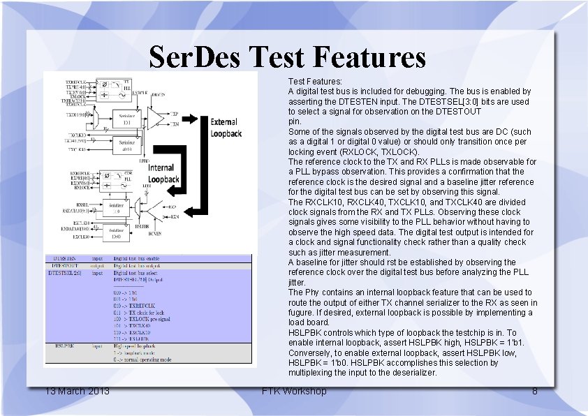
Ser. Des Test Features: A digital test bus is included for debugging. The bus is enabled by asserting the DTESTEN input. The DTESTSEL[3: 0] bits are used to select a signal for observation on the DTESTOUT pin. Some of the signals observed by the digital test bus are DC (such as a digital 1 or digital 0 value) or should only transition once per locking event (RXLOCK, TXLOCK). The reference clock to the TX and RX PLLs is made observable for a PLL bypass observation. This provides a confirmation that the reference clock is the desired signal and a baseline jitter reference for the digital test bus can be set by observing this signal. The RXCLK 10, RXCLK 40, TXCLK 10, and TXCLK 40 are divided clock signals from the RX and TX PLLs. Observing these clock signals gives some visibility to the PLL behavior without having to observe the high speed data. The digital test output is intended for a clock and signal functionality check rather than a quality check such as jitter measurement. A baseline for jitter should rst be established by observing the reference clock over the digital test bus before analyzing the PLL jitter. The Phy contains an internal loopback feature that can be used to route the output of either TX channel serializer to the RX as seen in fugure. If desired, external loopback is possible by implementing a load board. HSLPBK controls which type of loopback the testchip is in. To enable internal loopback, assert HSLPBK high, HSLPBK = 1'b 1. Conversely, to enable external loopback, assert HSLPBK low, HSLPBK = 1'b 0. HSLPBK accomplishes this selection by multiplexing the input to the deserializer. 13 March 2013 FTK Workshop 8

Ser. Des other Test Features TX Testing the transmitter can be accomplished by applying a stimulus and viewing the eye diagram on the oscilloscope. If the functionality is available, it is beneficial to see time interval errors due to the transmitter additive noise. The expected time interval error (TIE) due to the serializer and TX PLL should be less than 0. 01 UI from 100 k. Hz to 20 MHz. PRBS Testing In order to evaluate the quality of the serial link PRBS testing should be done using the PRBS-7 pattern from the pattern generator. To properly transmit the PRBS test pattern across the serial link, HSLPBK should be enabled. The serial bit rate should be swept from a value near the lower end of the specied range to a value near the maximum data transmission rate to stress the link and test its robustness. 13 March 2013 FTK Workshop 9

Amchip PCB Connection Test The Silicon Creation Ser. Des does not include JTAG (neither 1149. 1 nor 1149. 6) boundary scantest. The HSS conncetion test between AM chip on the PCB actually cannot be performed. In the IP it is not possible (and could be dangerous) to add boundary scan cells to the LVDS driver and receiver. To implement such a test other solutions can be used: ● Use PRBS test to check the conncetions ● Putting logical '1' at the input bus of the serdes and transmitting this data without 8 b/10 b coding. ● Generating a '101010' sequence at low frequency (perhaps 0. 1 KHz) and transmitting it without 8 b/10 b conding. All these solutions assumes that the serializer and deserializer on the AM chip work properly. This assumption should be correct because all chips are tested before mounting on the LAMB. Moreover, another assumpion is that the clock and high speed signal distribution on the LAMB board have to work properly. Actually no other solutions to test chip to chip connections are available. 13 March 2013 FTK Workshop 10

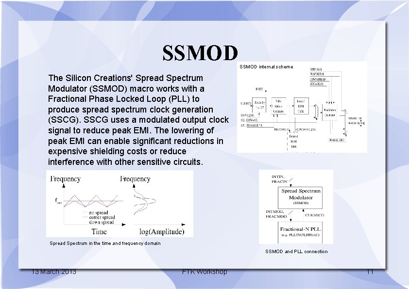
SSMOD internal scheme The Silicon Creations' Spread Spectrum Modulator (SSMOD) macro works with a Fractional Phase Locked Loop (PLL) to produce spread spectrum clock generation (SSCG). SSCG uses a modulated output clock signal to reduce peak EMI. The lowering of peak EMI can enable significant reductions in expensive shielding costs or reduce interference with other sensitive circuits. Spread Spectrum in the time and frequency domain SSMOD and PLL connection 13 March 2013 FTK Workshop 11

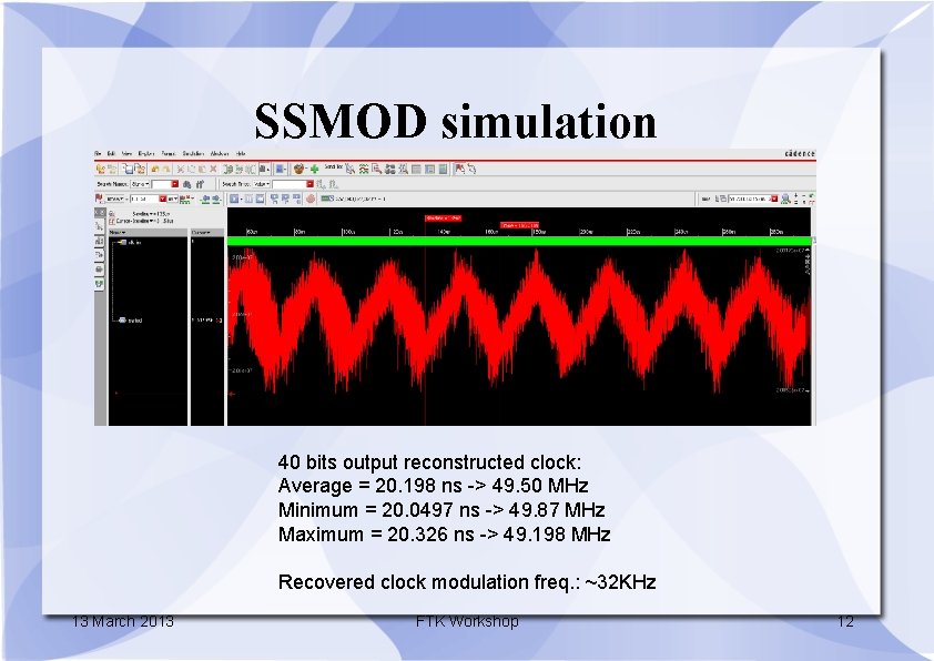
SSMOD simulation 40 bits output reconstructed clock: Average = 20. 198 ns -> 49. 50 MHz Minimum = 20. 0497 ns -> 49. 87 MHz Maximum = 20. 326 ns -> 49. 198 MHz Recovered clock modulation freq. : ~32 KHz 13 March 2013 FTK Workshop 12

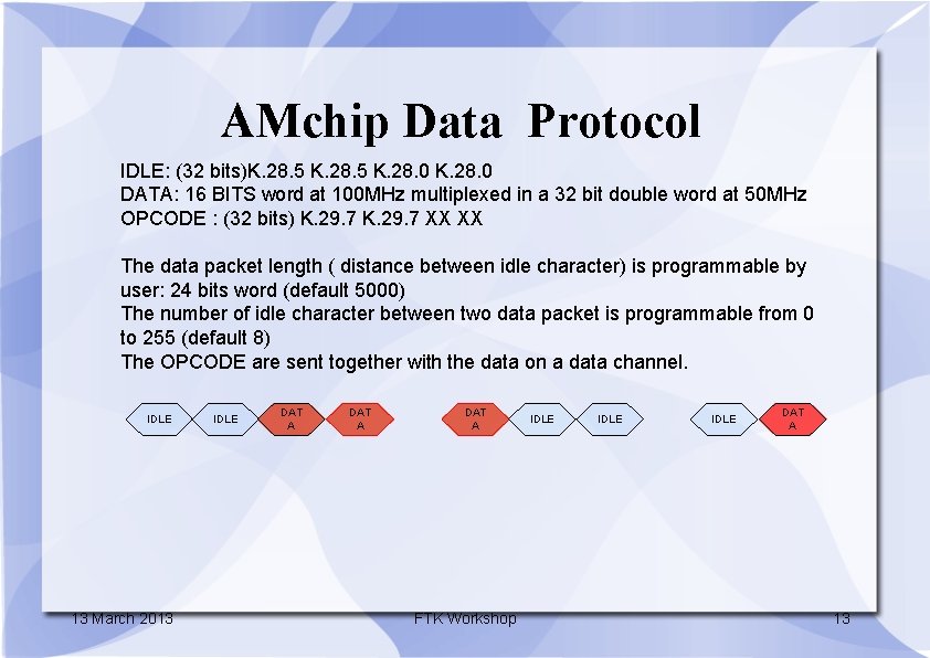
AMchip Data Protocol IDLE: (32 bits)K. 28. 5 K. 28. 0 DATA: 16 BITS word at 100 MHz multiplexed in a 32 bit double word at 50 MHz OPCODE : (32 bits) K. 29. 7 XX XX The data packet length ( distance between idle character) is programmable by user: 24 bits word (default 5000) The number of idle character between two data packet is programmable from 0 to 255 (default 8) The OPCODE are sent together with the data on a data channel. IDLE DAT A IDLE DAT A IDLE DAT A IDLE OPC ODE IDLE 13 March 2013 FTK Workshop 13

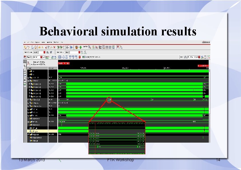
Behavioral simulation results 13 March 2013 FTK Workshop 14