The 8051 Microcontroller Chapter 2 HARDWARE SUMMARY The
- Slides: 24

The 8051 Microcontroller Chapter 2 HARDWARE SUMMARY

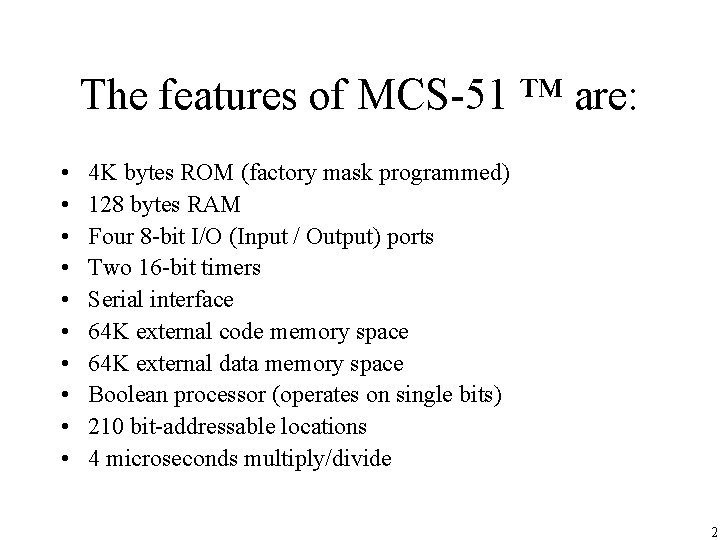
The features of MCS-51 ™ are: • • • 4 K bytes ROM (factory mask programmed) 128 bytes RAM Four 8 -bit I/O (Input / Output) ports Two 16 -bit timers Serial interface 64 K external code memory space 64 K external data memory space Boolean processor (operates on single bits) 210 bit-addressable locations 4 microseconds multiply/divide 2

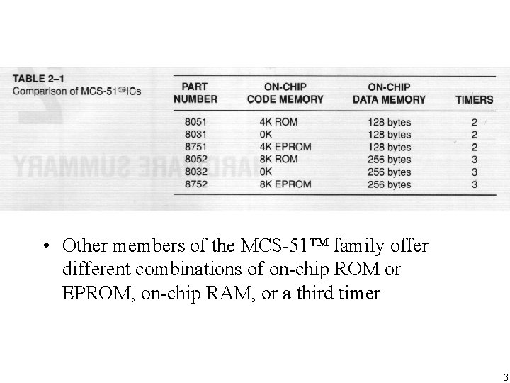
• Other members of the MCS-51™ family offer different combinations of on-chip ROM or EPROM, on-chip RAM, or a third timer 3

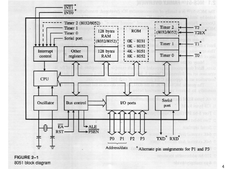
4

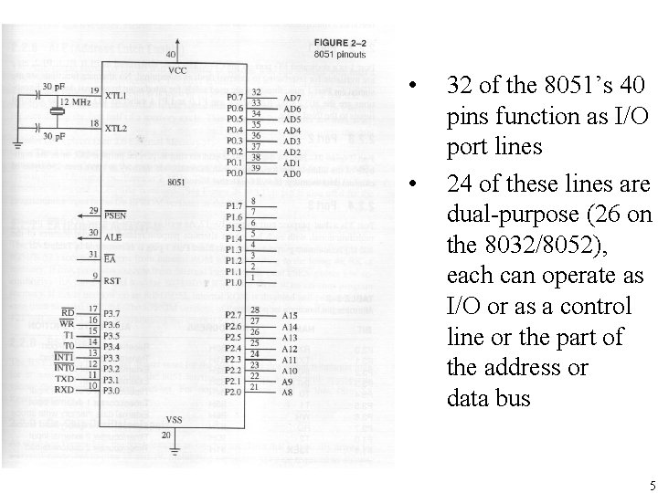
• • 32 of the 8051’s 40 pins function as I/O port lines 24 of these lines are dual-purpose (26 on the 8032/8052), each can operate as I/O or as a control line or the part of the address or data bus 5

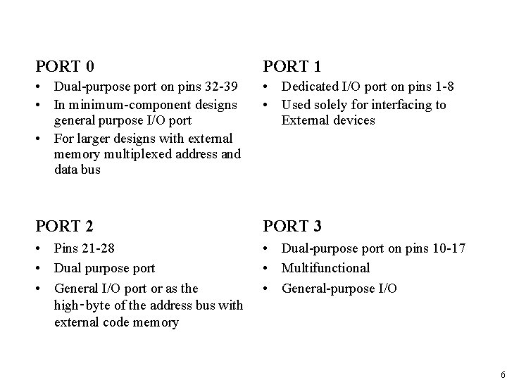
PORT 0 PORT 1 • Dual-purpose port on pins 32 -39 • In minimum-component designs general purpose I/O port • For larger designs with external memory multiplexed address and data bus • Dedicated I/O port on pins 1 -8 • Used solely for interfacing to External devices PORT 2 PORT 3 • Pins 21 -28 • Dual purpose port • General I/O port or as the high‑byte of the address bus with external code memory • Dual-purpose port on pins 10 -17 • Multifunctional • General-purpose I/O 6

7

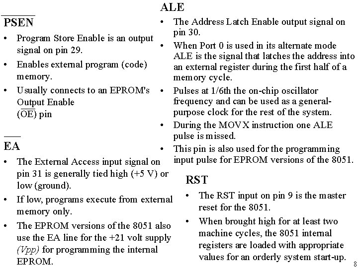
ALE • The Address Latch Enable output signal on pin 30. • Program Store Enable is an output • When Port 0 is used in its alternate mode signal on pin 29. ALE is the signal that latches the address into • Enables external program (code) an external register during the first half of a memory cycle. • Usually connects to an EPROM's • Pulses at 1/6 th the on-chip oscillator frequency and can be used as a general. Output Enable purpose clock for the rest of the system. (OE) pin • During the MOVX instruction one ALE pulse is missed. EA • This pin is also used for the programming • The External Access input signal on input pulse for EPROM versions of the 8051. pin 31 is generally tied high (+5 V) or RST low (ground). • If low, programs execute from external • The RST input on pin 9 is the master reset for the 8051. memory only. • The EPROM versions of the 8051 also • When brought high for at least two machine cycles, the 8051 internal use the EA line for the +21 volt supply registers are loaded with appropriate (Vpp) for programming the internal values for an orderly system start-up. EPROM. 8 PSEN

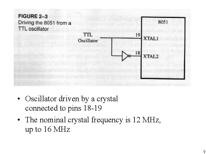
• Oscillator driven by a crystal connected to pins 18 -19 • The nominal crystal frequency is 12 MHz, up to 16 MHz 9

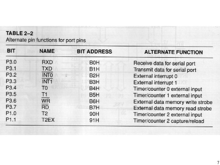
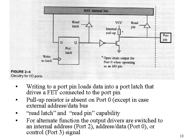
• • Writing to a port pin loads data into a port latch that drives a FET connected to the port pin Pull-up resistor is absent on Port 0 (except in case external address/data bus “read latch” and “read pin” capability For alternate function the output drivers are switched to an internal address (Port 2), address/data (Port 0), or control (Port 3) signal 10

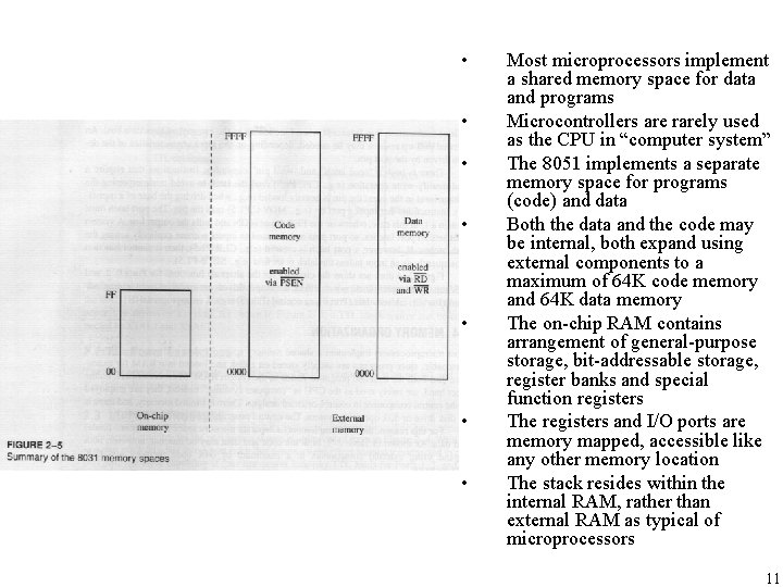
• • Most microprocessors implement a shared memory space for data and programs Microcontrollers are rarely used as the CPU in “computer system” The 8051 implements a separate memory space for programs (code) and data Both the data and the code may be internal, both expand using external components to a maximum of 64 K code memory and 64 K data memory The on-chip RAM contains arrangement of general-purpose storage, bit-addressable storage, register banks and special function registers The registers and I/O ports are memory mapped, accessible like any other memory location The stack resides within the internal RAM, rather than external RAM as typical of microprocessors 11

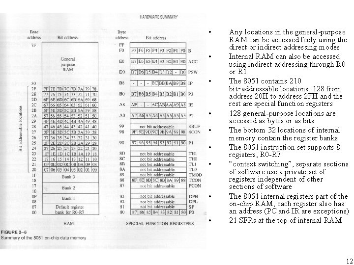
• • • Any locations in the general-purpose RAM can be accessed feely using the direct or indirect addressing modes Internal RAM can also be accessed using indirect addressing through R 0 or R 1 The 8051 contains 210 bit‑addressable locations, 128 from address 20 H to address 2 FH and the rest are special function registers 128 general-purpose locations are accessed as bytes or as bits The bottom 32 locations of internal memory contain the register banks The 8051 instruction set supports 8 registers, R 0 -R 7 “context switching”, separate sections of software use a private set of registers independent of other sections of software The 8051 internal registers part of the on-chip RAM, each register also has an address (PC and IR are exceptions) 21 SFRs at the top of internal RAM 12

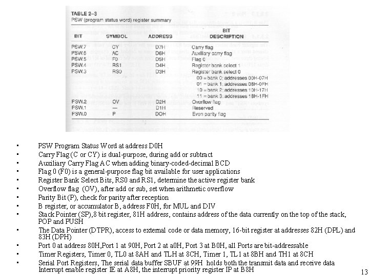
• • • • PSW Program Status Word at address D 0 H Carry Flag (C or CY) is dual-purpose, during add or subtract Auxiliary Carry Flag AC when adding binary-coded-decimal BCD Flag 0 (F 0) is a general-purpose flag bit available for user applications Register Bank Select Bits, RS 0 and RS 1, determine the active register bank Overflow flag (OV), after add or sub, set when arithmetic overflow Parity Bit (P), check for parity after reception B register, or accumulator B, address F 0 H, for MUL and DIV Stack Pointer (SP), 8 bit register, 81 H address, contains address of the data currently on the top of the stack, POP and PUSH The Data Pointer (DTPR), access to external code or data memory, 16 -bit register at addresses 82 H (DPL) and 83 H (DPH) Port 0 at address 80 H, Port 1 at 90 H, Port 2 at a 0 H, Port 3 at B 0 H, all Ports are bit-addressable Timer Registers, Timer 0, TL 0 at 8 AH and TLH at 8 CH, Timer 1, TL 1 at 8 BH and TH 1 at 8 CH Serial Port Registers, The serial data buffer SBUF at 99 H holds both the transmit data and receive data Interrupt enable register IE at A 8 H, the interrupt priority register IP at B 8 H 13

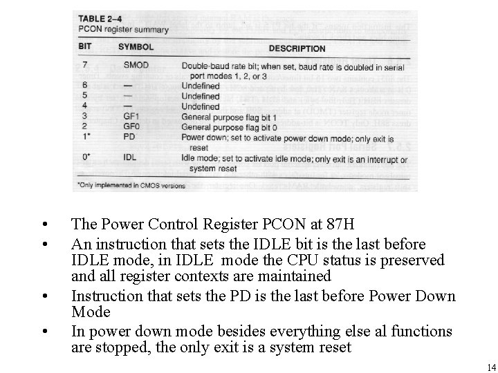
• • The Power Control Register PCON at 87 H An instruction that sets the IDLE bit is the last before IDLE mode, in IDLE mode the CPU status is preserved and all register contexts are maintained Instruction that sets the PD is the last before Power Down Mode In power down mode besides everything else al functions are stopped, the only exit is a system reset 14

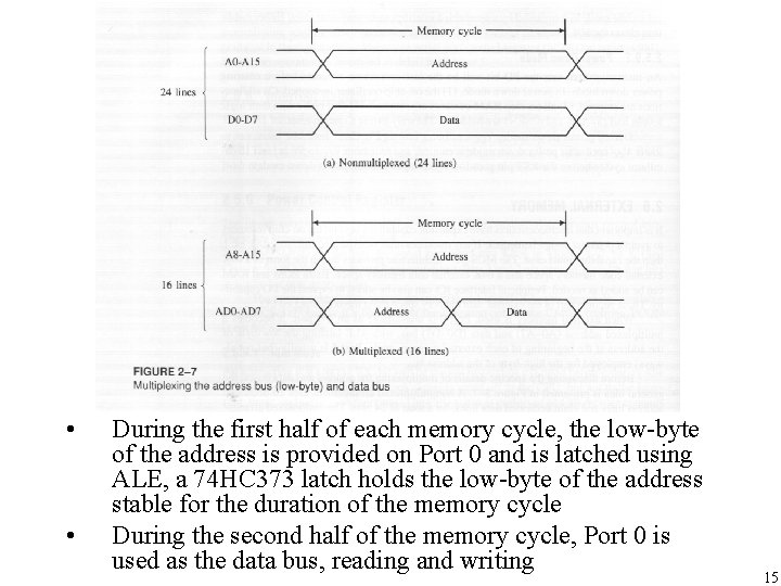
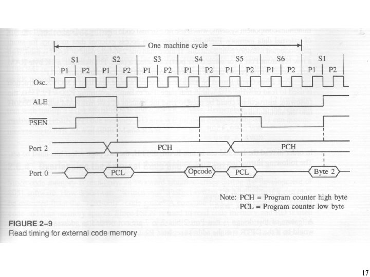
• • During the first half of each memory cycle, the low-byte of the address is provided on Port 0 and is latched using ALE, a 74 HC 373 latch holds the low-byte of the address stable for the duration of the memory cycle During the second half of the memory cycle, Port 0 is used as the data bus, reading and writing 15

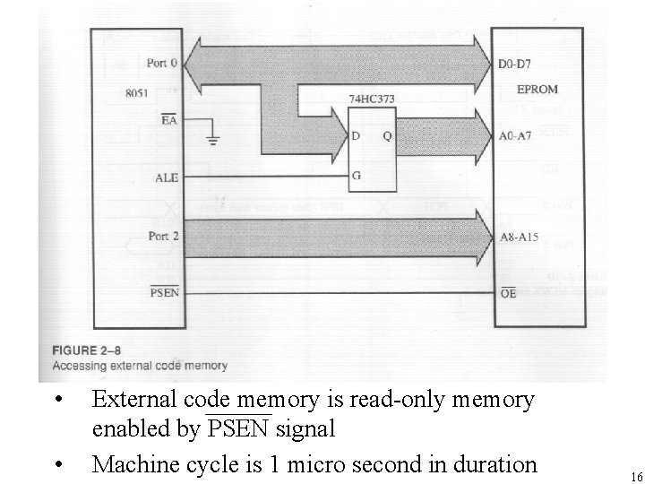
• • External code memory is read-only memory enabled by PSEN signal Machine cycle is 1 micro second in duration 16

17

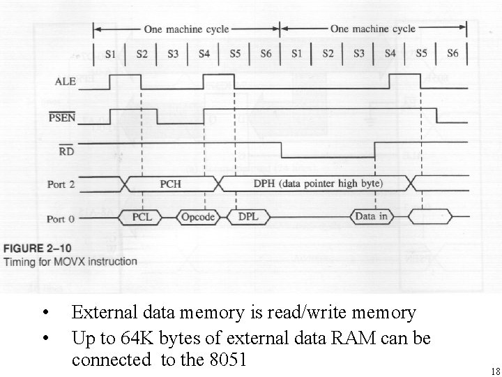
• • External data memory is read/write memory Up to 64 K bytes of external data RAM can be connected to the 8051 18

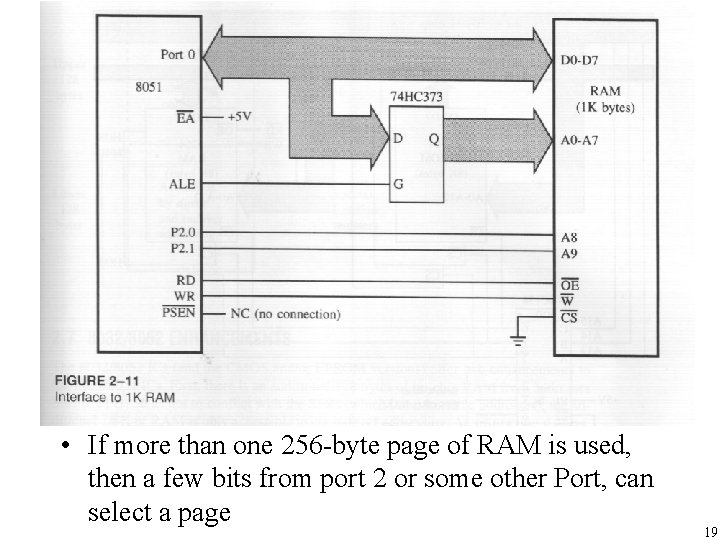
• If more than one 256 -byte page of RAM is used, then a few bits from port 2 or some other Port, can select a page 19

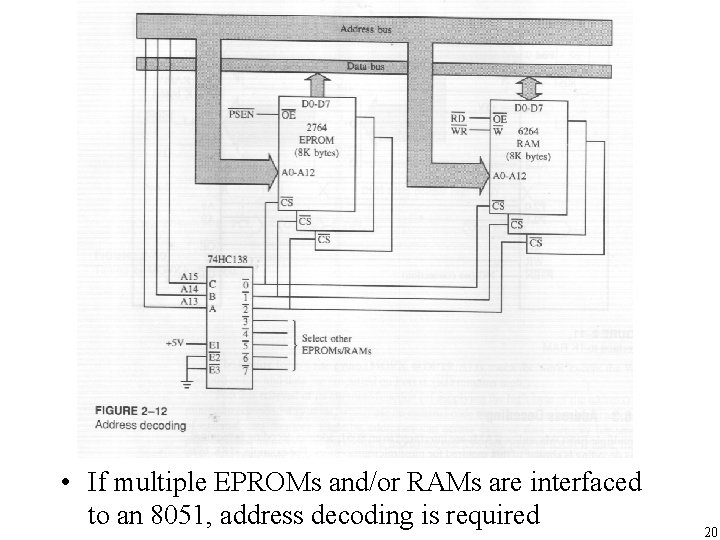
• If multiple EPROMs and/or RAMs are interfaced to an 8051, address decoding is required 20

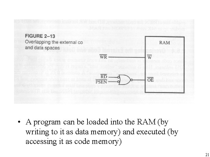
• A program can be loaded into the RAM (by writing to it as data memory) and executed (by accessing it as code memory) 21

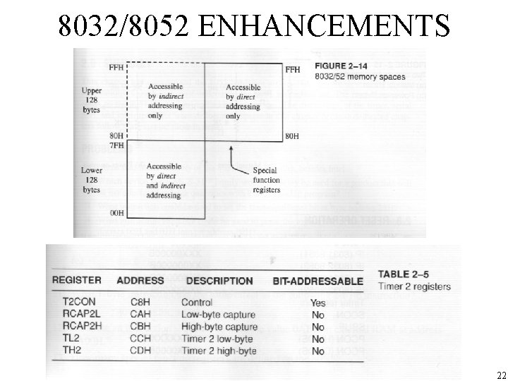
8032/8052 ENHANCEMENTS 22

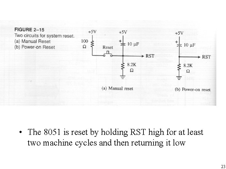
• The 8051 is reset by holding RST high for at least two machine cycles and then returning it low 23

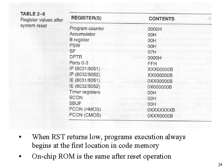
• • When RST returns low, programs execution always begins at the first location in code memory On-chip ROM is the same after reset operation 24