
Testing with the LV500 4 Tektronix LV500 4
- Slides: 78
Testing with the LV-500 4 Tektronix LV-500 4 Built in 1989 -1991 4 I. e. Ancient technology! 4 e. Bay is a good source for spare parts these days… 4 Specifically designed to be a stand-alone tester for ASICs 4 I. e. More testing features than a basic logic analyzer
What’s an ASIC Tester? 4 Ours is built on a Tektronix DAS 9200 logic analyzer platform 4 The main differences are in the test head, the pattern/error cards, and the Schmoo 4 The test head has up to 256 bi-directional pins where each pin has programmable electronics 4 voltage drive, current drive, voltage sense, etc. 4 The pattern/error cards store and compare the test vectors at up to 50 MHz 4 fast for 1989! 4 A Schmoo lets you run repeated tests while the tester alters one or two independent variables like threshold, delay, cycle length, voltage, etc.
Flavors of LV 500 s 4 Common Features 4 Test speeds up to 50 MHz 4 Up to 64, 000 unique test vectors 4 Network connection for uploading tests 4 Thinlan ethernet 48 Meg of RAM 421 or 43 Meg hard drive 45. 25 floppy (1. 2 M floppy)
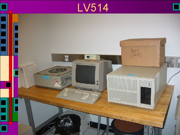
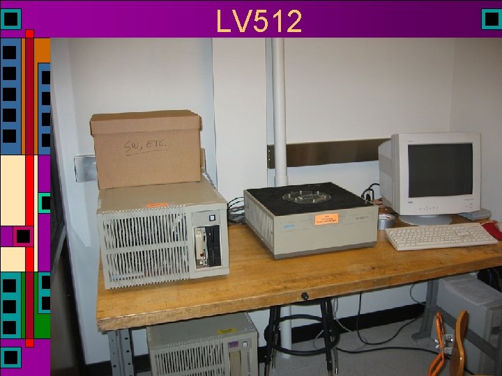
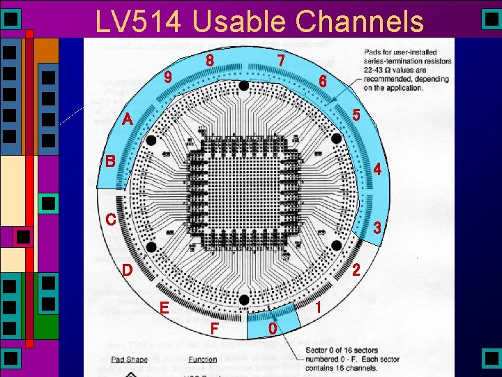
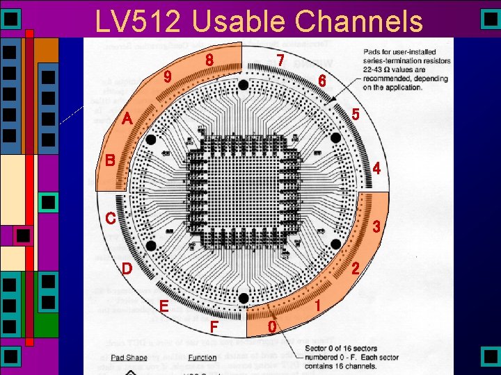
Flavors of LV 500 s 4 LV 514 4192 test channels (12 sectors) 4160 are usable (two sectors are bad) 4 Pre-wired test card for class chips 4(should really be called LV 513, but that’s a long story) 4 LV 512 4128 test channels (8 sectors) 4 All channels are usable 4 Used mostly for tutorial purposes 4 No pre-wired class chip test card yet…
LV 514
LV 512
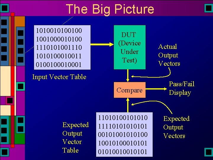
The Big Picture 101001000010100 1110101001110 101010011 010010001 DUT (Device Under Test) Input Vector Table Compare Expected Output Vector Table 110101010 1111010101 001010100 100101010010010101 Actual Output Vectors Pass/Fail Display Expected Output Vectors
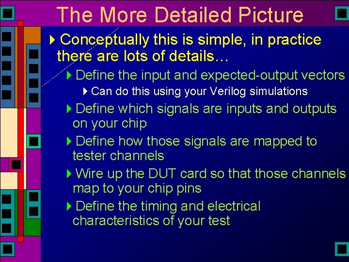
The More Detailed Picture 4 Conceptually this is simple, in practice there are lots of details… 4 Define the input and expected-output vectors 4 Can do this using your Verilog simulations 4 Define which signals are inputs and outputs on your chip 4 Define how those signals are mapped to tester channels 4 Wire up the DUT card so that those channels map to your chip pins 4 Define the timing and electrical characteristics of your test
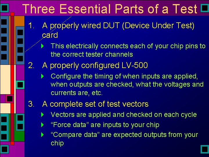
Three Essential Parts of a Test 1. A properly wired DUT (Device Under Test) card 4 This electrically connects each of your chip pins to the correct tester channels 2. A properly configured LV-500 4 Configure the timing of when inputs are applied, when outputs are checked, what the voltages and currents are, etc. 3. A complete set of test vectors 4 Vectors are applied and checked on each cycle 4 “Force data” are inputs to your chip 4 “Compare data” are expected outputs from your chip
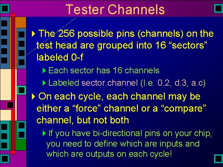
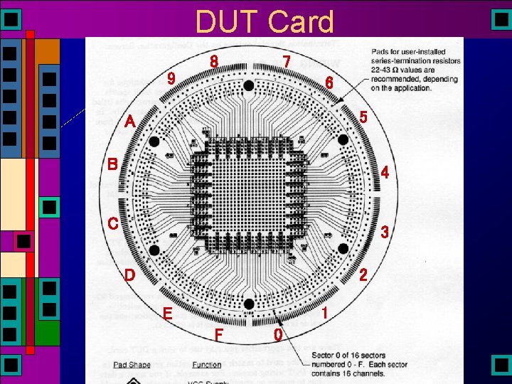
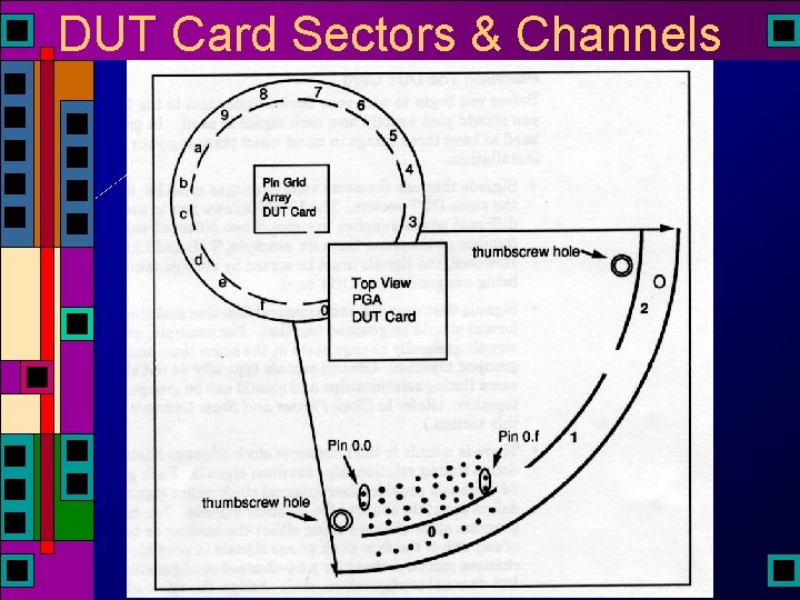
Tester Channels 4 The 256 possible pins (channels) on the test head are grouped into 16 “sectors” labeled 0 -f 4 Each sector has 16 channels 4 Labeled sector. channel (I. e. 0. 2, d. 3, a. c) 4 On each cycle, each channel may be either a “force” channel or a “compare” channel, but not both 4 If you have bi-directional pins on your chip, you need to define which are inputs and which are outputs on each cycle!
DUT Card 8 7 9 6 5 A B 4 C 3 D 2 E 1 F 0
LV 514 Usable Channels 8 7 9 6 5 A B 4 C 3 D 2 E 1 F 0
LV 512 Usable Channels 8 7 9 6 5 A B 4 C 3 D 2 E 1 F 0
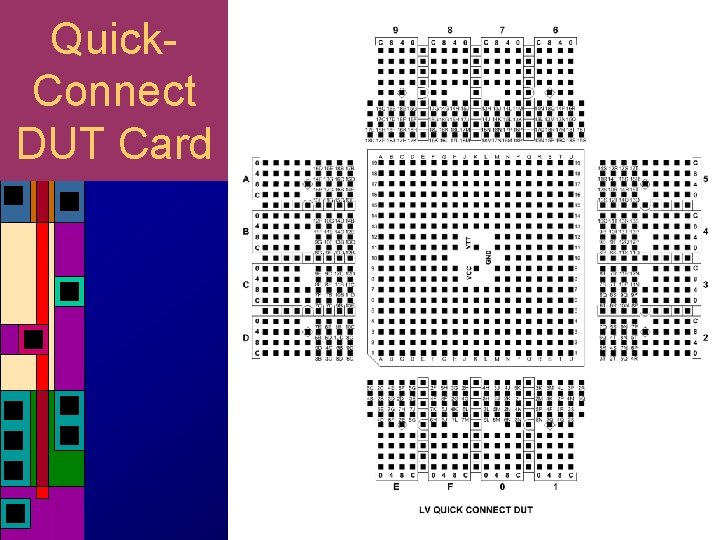
DUT Card Sectors & Channels
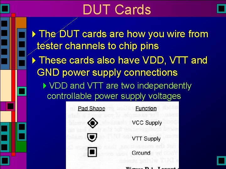
DUT Cards 4 The DUT cards are how you wire from tester channels to chip pins 4 These cards also have VDD, VTT and GND power supply connections 4 VDD and VTT are two independently controllable power supply voltages
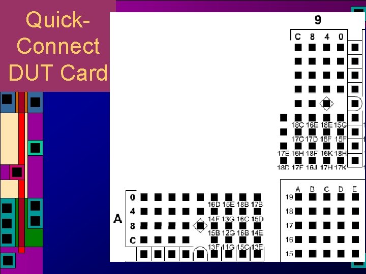
Wiring the DUT Card 4 Essentially two choices: 4 Solder wires on a PGA DUT card 4 Remember that VDD and GND are not connected to tester channels 4 Probably only want to do this once for the whole class 4 Which means standardizing VDD and GND! 4 Use a “Quick-Connect” card 4 Uses 3 M Scotch-Connect to wire (using wirewrap wire) from the tester channels to the chip socket 4 Can also use quick-connect for VDD and GND
Quick. Connect DUT Card
Quick. Connect DUT Card
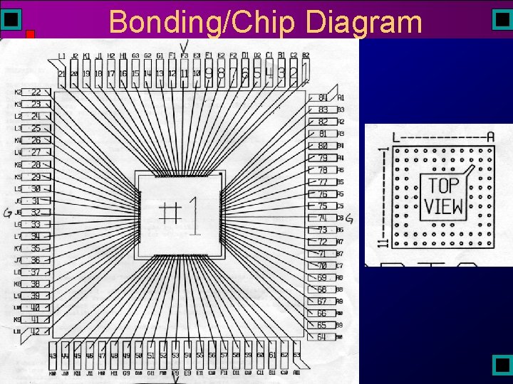
Knowing What to Wire 4 A “Bonding Diagram” is a picture that shows how your chip was bonded to the chip frame 4 It also shows how the chip frame is connected to the chip pins
Bonding/Chip Diagram
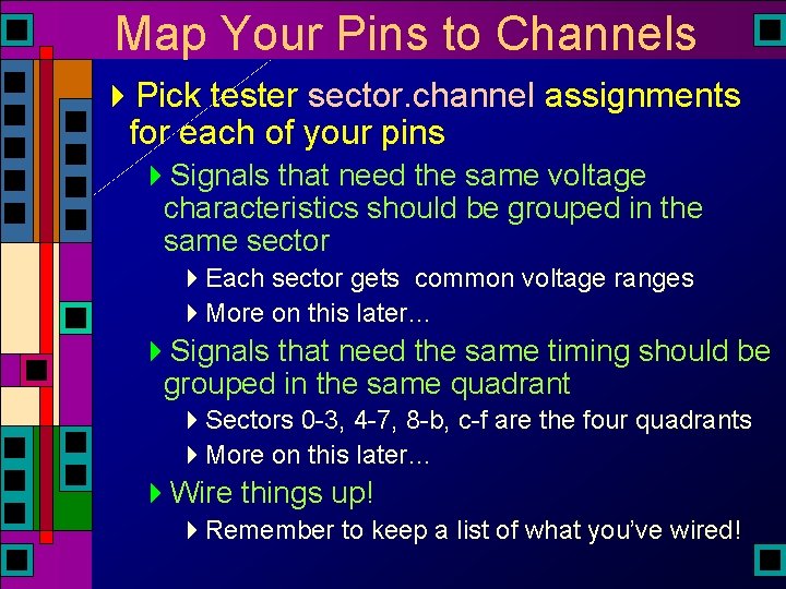
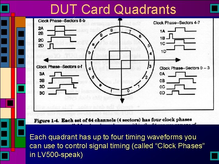
Map Your Pins to Channels 4 Pick tester sector. channel assignments for each of your pins 4 Signals that need the same voltage characteristics should be grouped in the same sector 4 Each sector gets common voltage ranges 4 More on this later… 4 Signals that need the same timing should be grouped in the same quadrant 4 Sectors 0 -3, 4 -7, 8 -b, c-f are the four quadrants 4 More on this later… 4 Wire things up! 4 Remember to keep a list of what you’ve wired!
Class DUT Card 4 Pre-wired for class chips 484 pin PGA with specific VDD and GND placements in the pad ring 4/usr/local/contrib/elb/lv 500/DUTmap. txt
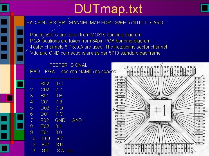
DUTmap. txt PAD-PIN-TESTER CHANNEL MAP FOR CS/EE 5710 DUT CARD Pad locations are taken from MOSIS bonding diagram PGA locations are taken from 84 pin PGA bonding diagram Tester channels 6, 7, 8, 9, A are used. The notation is sector. channel Vdd and GND connections are as per 5710 standard pad frame TESTER SIGNAL PAD PGA sec. chn NAME (no spaces) ----------------1 B 02 6. C 2 C 02 7. 7 3 B 01 6. B 4 C 01 7. 6 5 D 02 7. D 6 D 01 7. C 7 F 02 GND 8 E 02 8. 1 9 E 01 8. 0 10 E 03 8. 7 12 F 01 8. 6 13 G 01 8. A etc….
Finished DUT Card 4 Now you have part 1 – a wired DUT card that connects your chip to the tester 4 On to part 2 – configuring the tester…
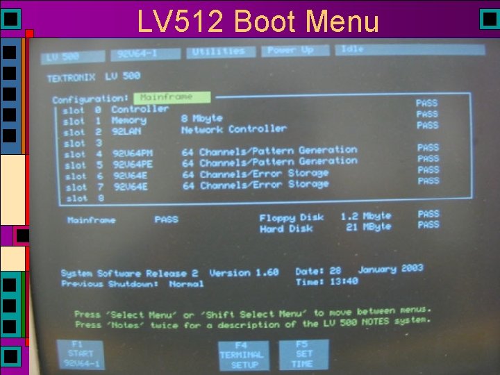
LV 512 Boot Menu
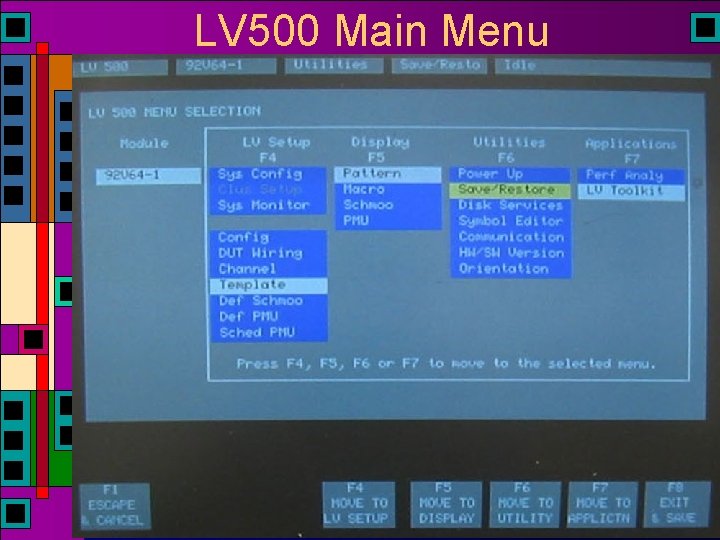
LV 500 Main Menu
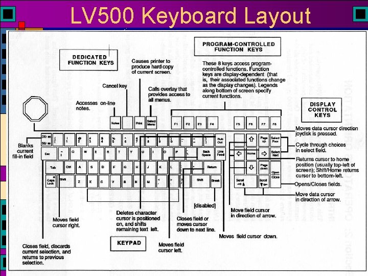
LV 500 Keyboard Layout
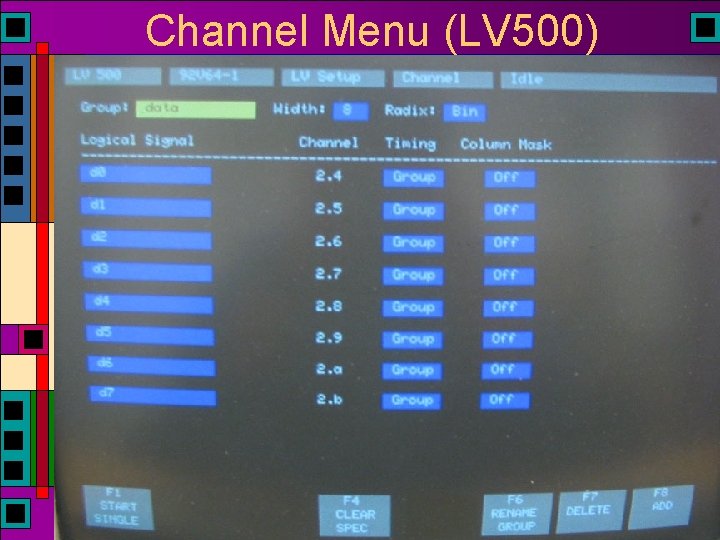
Important Menu Choices 4 Config Menu 4 Defines voltages for VDD, VTT, GND 4 Defines voltages for two force/compare sets 4 DUT Wiring menu 4 Defines how your signals are assigned to tester sector. channels 4 Channel menu 4 Defines how your signals are collected into groups (I. e. buses) 4 ALL signals must be a part of some group 4 Groups are assigned to specific timing templates (clock phases)
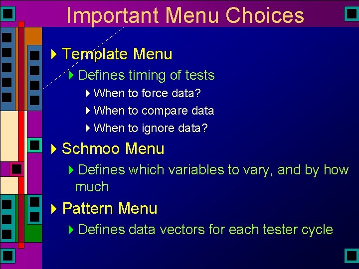
Important Menu Choices 4 Template Menu 4 Defines timing of tests 4 When to force data? 4 When to compare data 4 When to ignore data? 4 Schmoo Menu 4 Defines which variables to vary, and by how much 4 Pattern Menu 4 Defines data vectors for each tester cycle
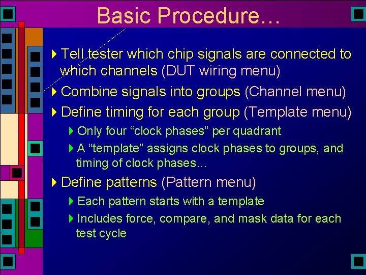
Basic Procedure… 4 Tell tester which chip signals are connected to which channels (DUT wiring menu) 4 Combine signals into groups (Channel menu) 4 Define timing for each group (Template menu) 4 Only four “clock phases” per quadrant 4 A “template” assigns clock phases to groups, and timing of clock phases… 4 Define patterns (Pattern menu) 4 Each pattern starts with a template 4 Includes force, compare, and mask data for each test cycle
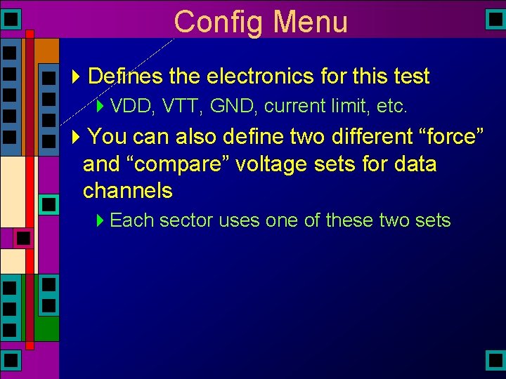
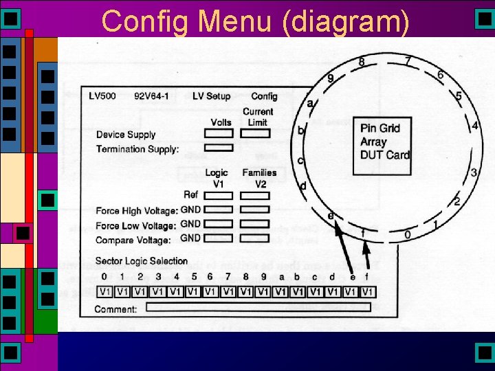
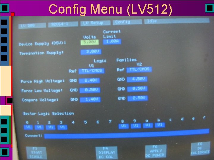
Config Menu 4 Defines the electronics for this test 4 VDD, VTT, GND, current limit, etc. 4 You can also define two different “force” and “compare” voltage sets for data channels 4 Each sector uses one of these two sets
Config Menu (diagram)
Config Menu (LV 512)
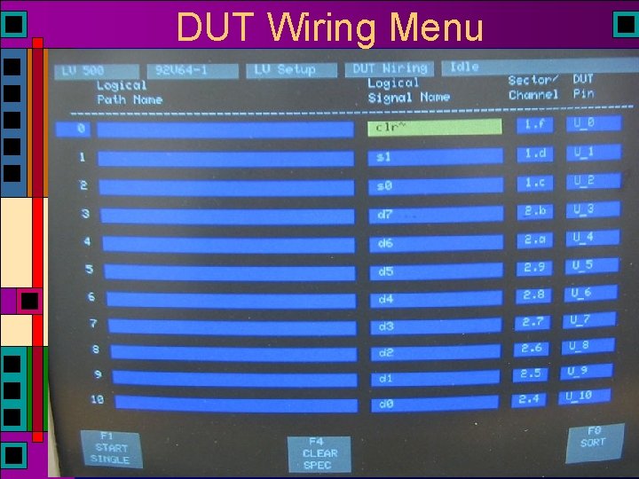
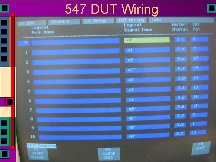
DUT Wiring Menu 4 Defines how your signals are assigned to tester sector. channels 4 List signal names 4 Define which tester channels they connect to 4 Optionally define which actual chip (DUT) pins they are connected to 4 This is just a comment for documentation
DUT Wiring Menu
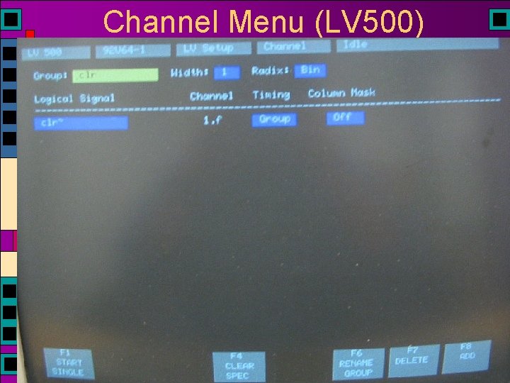
Channel Menu 4 Defines how your signals are collected into groups 4 EVERY signal must be a part of some group (even single signals) 4 Groups can make data entry and evaluation easier 4 Can define how group data is printed 4 Dec, Hex, Oct, Bin 4 Can specify timing once for the whole group 4 In general, inputs vs. outputs is a good group… 4 Or control vs. data, etc.
Channel Menu (LV 500)
Channel Menu (LV 500)
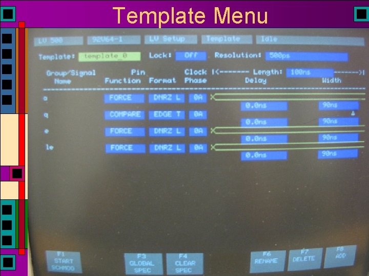
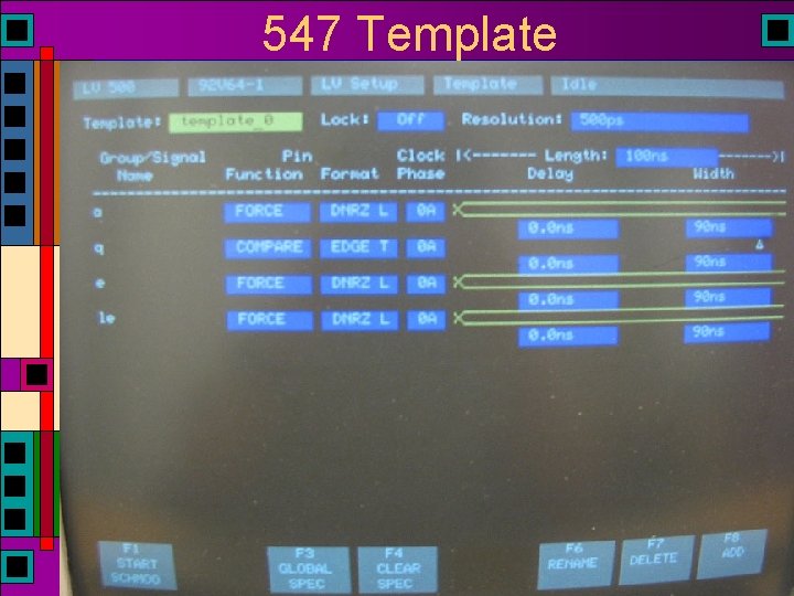
Templates 4 Defines timing of tests 4 When to force data? 4 When to compare data 4 When to ignore data? 4 Set up using a “clock phase” 4 Bad name – really a timing waveform 4 Defines when things happen in each tester cycle 4 You can define up to four clock phases per quadrant
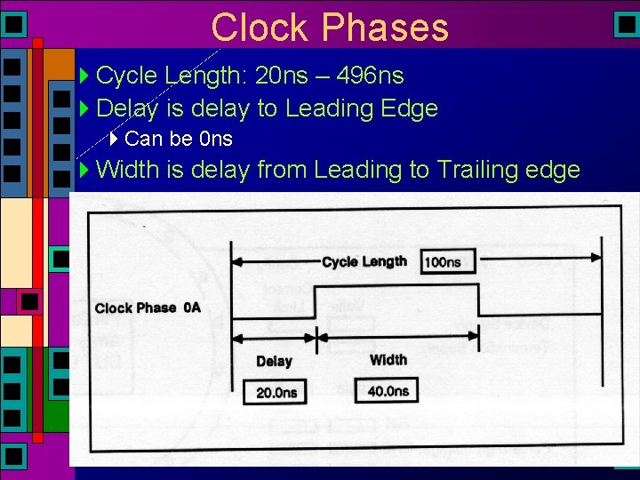
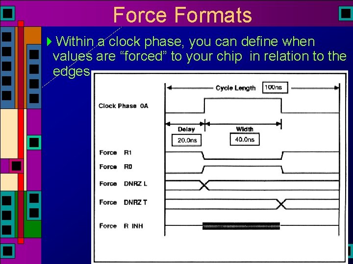
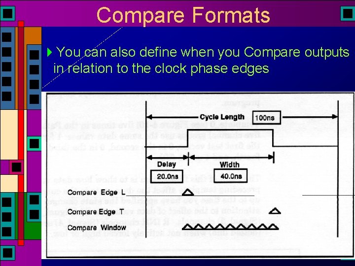
Clock Phases 4 Cycle Length: 20 ns – 496 ns 4 Delay is delay to Leading Edge 4 Can be 0 ns 4 Width is delay from Leading to Trailing edge
DUT Card Quadrants Each quadrant has up to four timing waveforms you can use to control signal timing (called “Clock Phases” in LV 500 -speak)
Force Formats 4 Within a clock phase, you can define when values are “forced” to your chip in relation to the edges
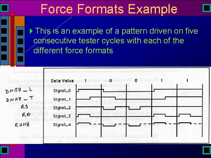
Force Formats Example 4 This is an example of a pattern driven on five consecutive tester cycles with each of the different force formats
Compare Formats 4 You can also define when you Compare outputs in relation to the clock phase edges
Template Menu
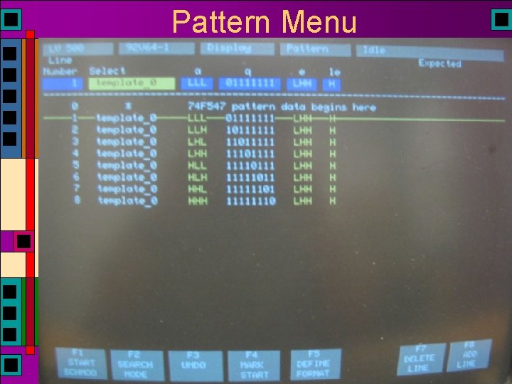
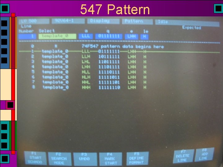
Pattern Menu 4 Defines data vectors for each tester cycle 4 Data for each signal is defined in the data vector 4 Some of those signals are “Force”, some are “Compare” and some are “Mask” 4 These are set in the templates 4 Assign a template to each vector 4 On each tester cycle, the next vector, with that vector’s template, is applied to the DUT and compared
Pattern Menu
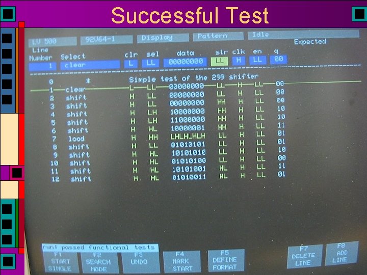
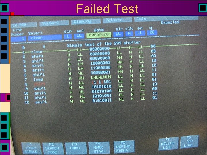
Pattern Display 4 The Pattern screen is where you see the results of your test 4 Before the test you can see all the vectors (and their templates) that you will be using 4 After running the test you see the same display with any errors highlighted in red 4 Red means that the output of the DUT didn’t match the expected output vector 4 You run the test with F 1 -Start (the F 1 function key)
Successful Test
Failed Test
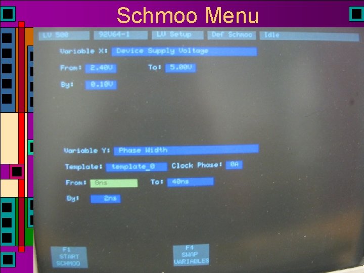
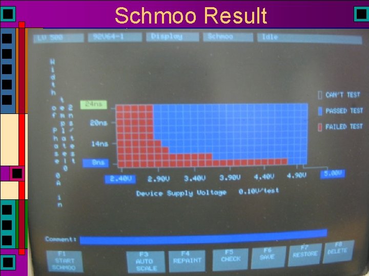
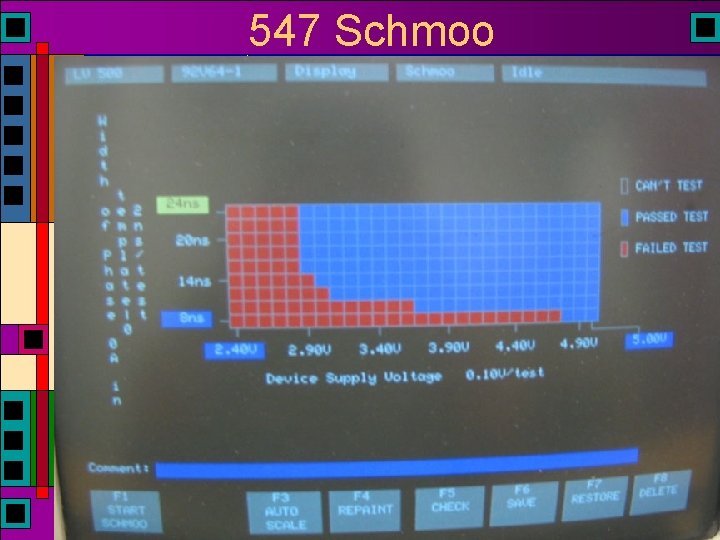
Schmoo Menu 4 After you have your basic test working, you can run a Schmoo test 4 Repeat the test while changing 1 or 2 variables 4 Variables can be things like VDD voltage, delay time, cycle time. Compare voltage, etc. 4 Generates a graph showing where the part worked or didn’t work
Schmoo Menu
Schmoo Result
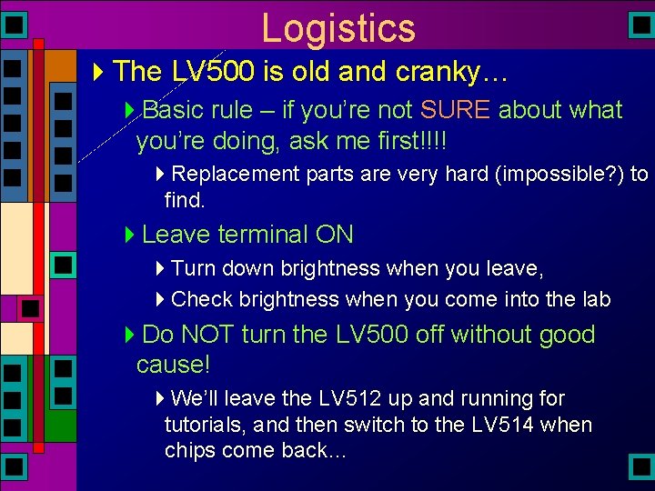
Logistics 4 The LV 500 is old and cranky… 4 Basic rule – if you’re not SURE about what you’re doing, ask me first!!!! 4 Replacement parts are very hard (impossible? ) to find. 4 Leave terminal ON 4 Turn down brightness when you leave, 4 Check brightness when you come into the lab 4 Do NOT turn the LV 500 off without good cause! 4 We’ll leave the LV 512 up and running for tutorials, and then switch to the LV 514 when chips come back…
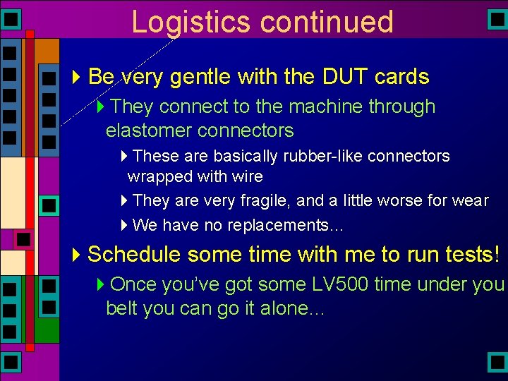
Logistics continued 4 Be very gentle with the DUT cards 4 They connect to the machine through elastomer connectors 4 These are basically rubber-like connectors wrapped with wire 4 They are very fragile, and a little worse for wear 4 We have no replacements… 4 Schedule some time with me to run tests! 4 Once you’ve got some LV 500 time under you belt you can go it alone…
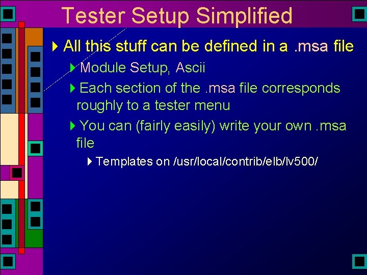
Tester Setup Simplified 4 All this stuff can be defined in a. msa file 4 Module Setup, Ascii 4 Each section of the. msa file corresponds roughly to a tester menu 4 You can (fairly easily) write your own. msa file 4 Templates on /usr/local/contrib/elb/lv 500/
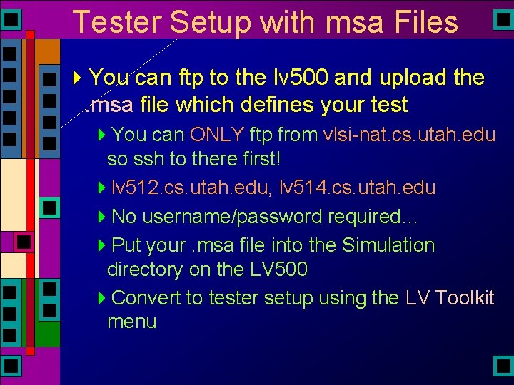
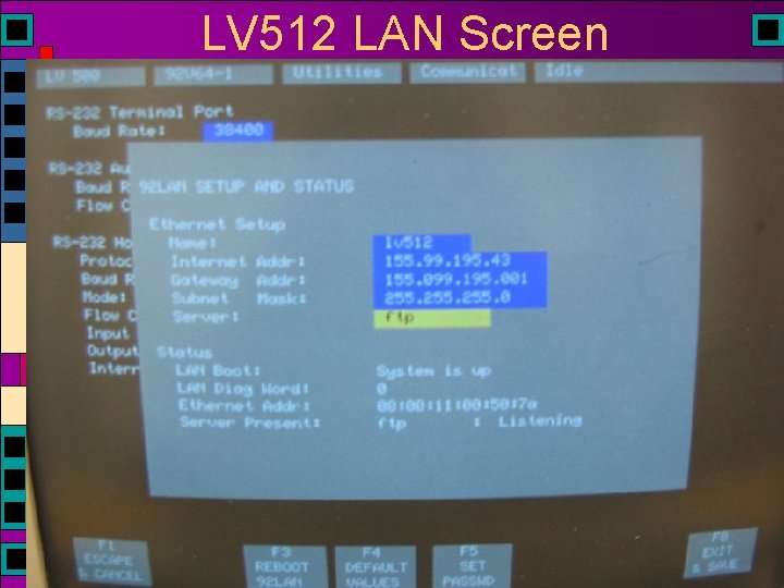
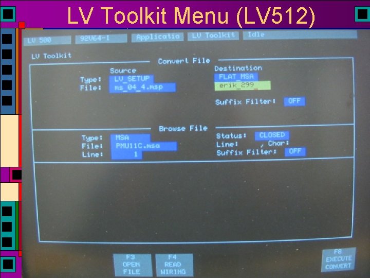
Tester Setup with msa Files 4 You can ftp to the lv 500 and upload the. msa file which defines your test 4 You can ONLY ftp from vlsi-nat. cs. utah. edu so ssh to there first! 4 lv 512. cs. utah. edu, lv 514. cs. utah. edu 4 No username/password required… 4 Put your. msa file into the Simulation directory on the LV 500 4 Convert to tester setup using the LV Toolkit menu
LV 512 LAN Screen
LV Toolkit Menu (LV 512)
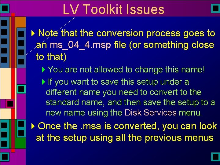
LV Toolkit Issues 4 Note that the conversion process goes to an ms_04_4. msp file (or something close to that) 4 You are not allowed to change this name! 4 If you want to save this setup under a different name you need to convert to the standard name, and then save the setup to a new name using the Disk Services menu. 4 Once the. msa is converted, you can look at the setup using all the previous menus
Running Tests 4 The. msa conversion is a great first step 4 But, after that’s running you may want to change things or try new things 4 Like Schmoo, or changing parameters 4 You can change the data using the menus shown earlier 4 You can also save the changed tests into new. msa files 4 And you can retrieve those new. msa files using FTP if you like
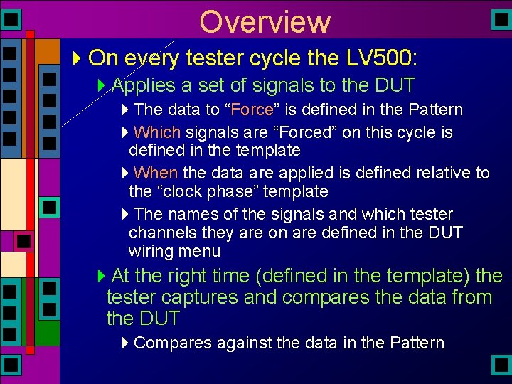
Overview 4 On every tester cycle the LV 500: 4 Applies a set of signals to the DUT 4 The data to “Force” is defined in the Pattern 4 Which signals are “Forced” on this cycle is defined in the template 4 When the data are applied is defined relative to the “clock phase” template 4 The names of the signals and which tester channels they are on are defined in the DUT wiring menu 4 At the right time (defined in the template) the tester captures and compares the data from the DUT 4 Compares against the data in the Pattern
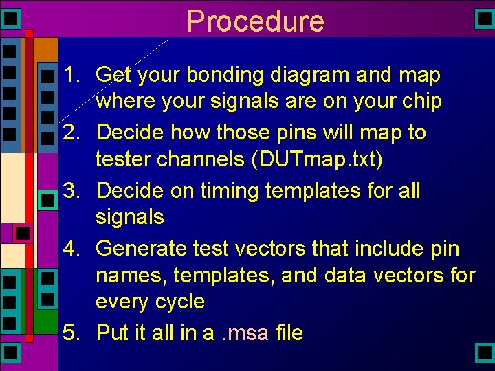
Procedure 1. Get your bonding diagram and map where your signals are on your chip 2. Decide how those pins will map to tester channels (DUTmap. txt) 3. Decide on timing templates for all signals 4. Generate test vectors that include pin names, templates, and data vectors for every cycle 5. Put it all in a. msa file
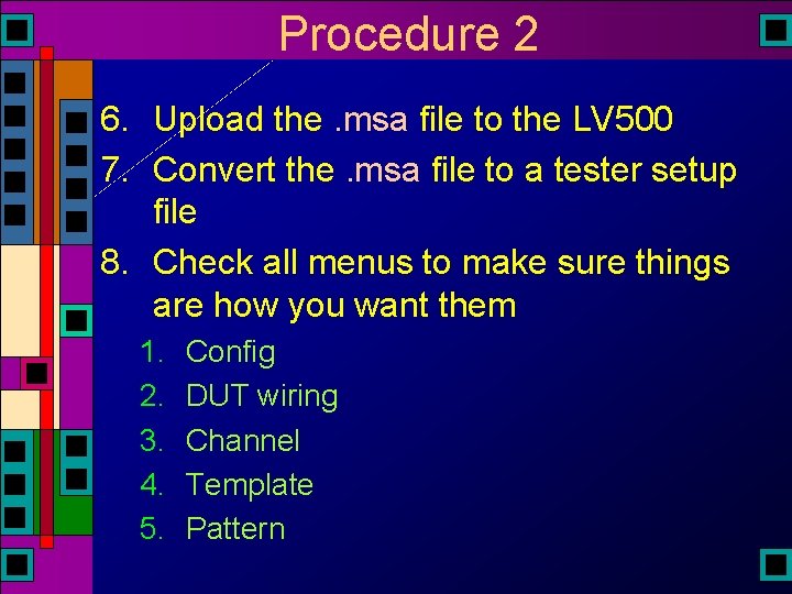
Procedure 2 6. Upload the. msa file to the LV 500 7. Convert the. msa file to a tester setup file 8. Check all menus to make sure things are how you want them 1. 2. 3. 4. 5. Config DUT wiring Channel Template Pattern
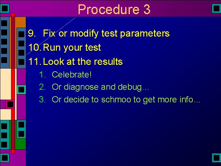
Procedure 3 9. Fix or modify test parameters 10. Run your test 11. Look at the results 1. Celebrate! 2. Or diagnose and debug… 3. Or decide to schmoo to get more info…
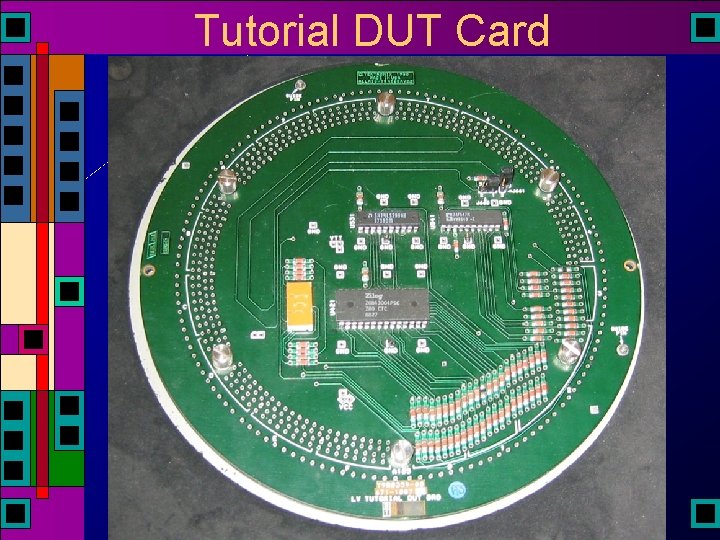
Tutorial DUT Card
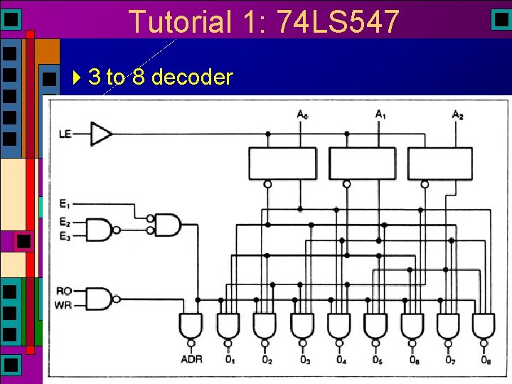
Tutorial 1: 74 LS 547 43 to 8 decoder
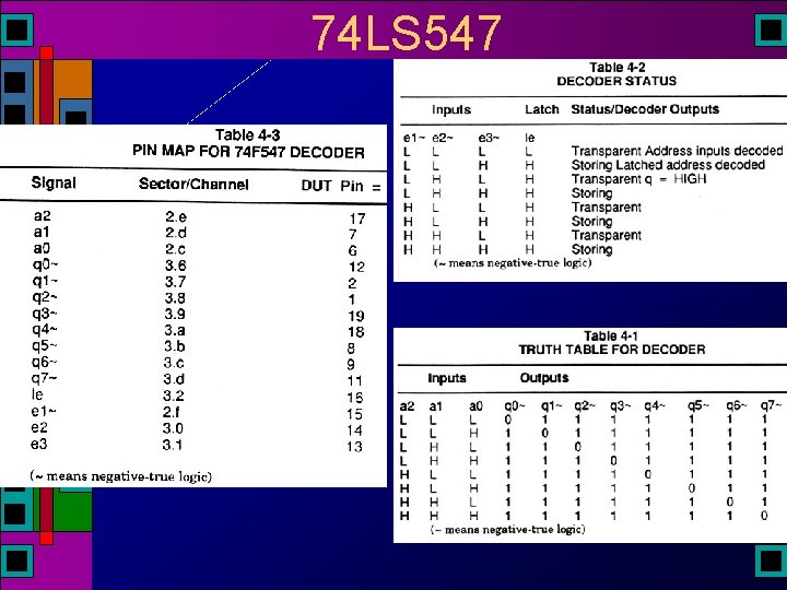
74 LS 547
547 DUT Wiring
547 Template
547 Pattern
547 Schmoo
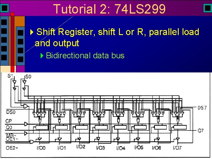
Tutorial 2: 74 LS 299 4 Shift Register, shift L or R, parallel load and output 4 Bidirectional data bus
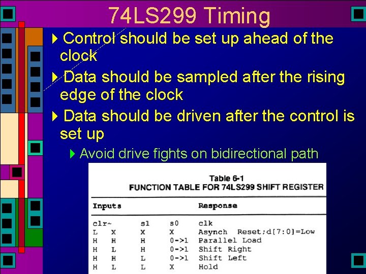
74 LS 299 Timing 4 Control should be set up ahead of the clock 4 Data should be sampled after the rising edge of the clock 4 Data should be driven after the control is set up 4 Avoid drive fights on bidirectional path
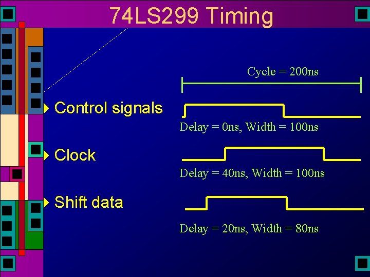
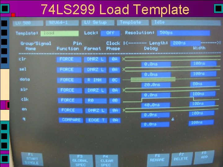
74 LS 299 Timing Cycle = 200 ns 4 Control signals Delay = 0 ns, Width = 100 ns 4 Clock Delay = 40 ns, Width = 100 ns 4 Shift data Delay = 20 ns, Width = 80 ns
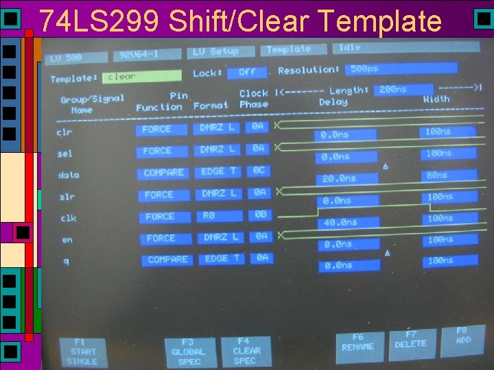
74 LS 299 Shift/Clear Template
74 LS 299 Load Template
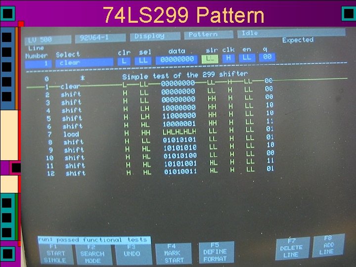
74 LS 299 Pattern