TESTING CMOS TESTING Levels of Testing Early detection


, to")


: - Three approaches • Adhoc Testing • Scan based testing")


")

 – System Level Test Technique")
 adjacent to each component pin")
- Slides: 30
TESTING
CMOS TESTING
Levels of Testing Early detection of faults reduce manufacturing costs.
TESTS FUNCTIONALITY TESTS MANUFACTURING TESTS
MANUFACTURING DEFECTS Defects in Si substrate, Photolithographic defects, Mask contamination & scratches, Process variations, Oxide defects Effects of Defects: Ø Ø Ø Layer to layer shorts Discontinuous wires - opens Thinox short to substrate or well Nodes shorted to power or ground Nodes shorted to each other Inputs floating / outputs disconnected.
Failures in CMOS
Physical defect in NOR gate fabrication Its electrical fault model
MANUFACTURING TEST PRINCIPLES FAULT MODELS STUCK AT FAULTS STUCK AT 1 MODEL STUCK AT 0 MODEL SHORT CIRCUIT AND OPEN CIRCUIT FAULTS STUCK OPEN MODEL SHORTED MODEL
MANUFACTURING TEST PRINCIPLES Testability - The ability for a Device Under Test (DUT), to be better observed and controlled easily from its external environment Controllability: The controllability of an internal circuit node within a chip is a measure with which the Test Engineer can establish a specific signal value at that node. Observability: Measure of the ease with which one can determine the signal value at any internal logic node in the circuit by controlling its primary input and observing the primary output. % Fault Coverage: (Number of faults detected when SA 0 + Number of faults detected when SA 1) / Total number of nodes in circuit
TESTING Combinational Logic Testing Exhaustive Testing Sensitized Path Testing
Combinational Logic Testing
Sensitized Path Testing : - D-Algorithm for ATPG In exhaustive testing, many patterns do not occur during the application of the circuit. So instead of spending a huge amount of time searching for faults everywhere, the possible faults are first enumerated and a set of appropriate vectors are then generated. This is called "single-path sensitization" and it is based on "fault oriented testing".
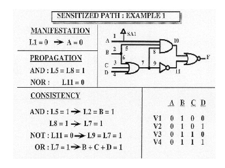
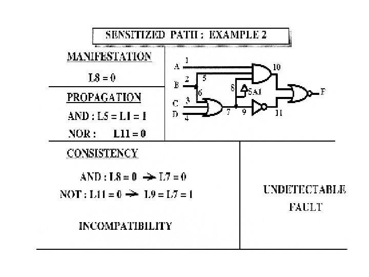
Sensitized Path Testing Select a path from the site of a fault, connecting the faulty node to the primary output. This path is called sensitized path. The process is composed of three steps : • Manifestation : gate inputs, at the site of the fault, are specified as to generate the opposite value of the faulty value (0 for SA 1, 1 for SA 0). • Propagation : inputs of the other gates are determined so as to propagate the fault signal along the specified path to the primary output of the circuit. This is done by setting these inputs to "1" for AND/NAND gates and "0" for OR/NOR gates. • Consistency : or justification. This final step helps finding the primary input pattern that will realize all the necessary input values. This is done by tracing backward from the gate inputs to the primary inputs of the logic in order to receive the test patterns.
Design Strategies for Test All "design for test" methods ensure that a design has enough observability and controllability to provide for a complete and efficient testing. When a node has difficult access from primary inputs or outputs (pads of the circuit), a very efficient method is to add internal pads in between the two blocks eg. to control block B 2 and observe block B 1 with a probe.
Design for Testability (DFT): - Three approaches • Adhoc Testing • Scan based testing • Self Test and Built In Self Test (BIST) Ad – hoc Testing Involves Partitioning Large sequential circuits Adding Test Points Adding Multiplexers Providing for easy state reset
ADHOC TESTING TECHNIQUES
ADHOC TESTING TECHNIQUES
ADHOC TESTING TECHNIQUES
ADHOC TESTING TECHNIQUES
ADHOC TESTING TECHNIQUES When a clock signal is gated with any data signal, for example a load signal coming from a tester, a skew or any other hazard on that signal can cause an error on the output of logic.
ADHOC TESTING TECHNIQUES
Disadvantages of ad-hoc DFT methods: 1. Experts and tools not always available. 2. Test generation is often manual with no guarantee of high fault coverage. 3. Design iterations may be necessary. Scan Based Design Technique - Advantages 1. Simple read/write access to all or subset of storage elements in a design. 2. Direct control of storage elements to an arbitrary value (0 or 1). 3. Direct observation of the state of storage elements and hence the internal state of the circuit. 4. Enhanced controllability and observability.
Scan Based Techniques
The method of testing a circuit with the scan path is as follows: 1. 2. 3. 4. 5. Set test mode signal, flip-flops accept data from input scan-in Verify the scan path by shifting in and out test data Set the shift register to an initial state Apply a test pattern to the primary inputs of the circuit Set normal mode, the circuit settles and can monitor the primary outputs of the circuit 6. Activate the circuit clock for one cycle 7. Return to test mode 8. Scan out the contents of the registers, simultaneously scan in the next pattern
Self Test Techniques 1. Signature Analysis and BILBO Uses Pseudo random Sequence generator (PRSG) to generate input signals for a section of combinational circuit and then uses a signature analyser to observe the output signals PRSG Combinational Circuit Signature Analyzer 2. Memory Self Test 3. IDDQ Testing – Used for testing bridging faults in CMOS
Chip Level Test Techniques 1. Logic structures such as datapaths use partial serial scan or parallel scan 2. Random logic tested via full serial scan or parallel scan
Boundary Scan Test (BST) – System Level Test Technique
BST consists in placing a scan path (shift register) adjacent to each component pin and to interconnect the cells in order to form a chain around the border of the circuit. The BST circuits contained on one board are then connected together to form a single path through the board. The boundary scan path is provided with serial input and output pads and appropriate clock pads which make it possible to : 1. Test the interconnections between the various chip 2. Deliver test data to the chips on board for self-testing 3. Test the chips themselves with internal self-test Advantages of Boundary scan techniques: 1. No need for complex testers in PCB testing 2. Test engineers work is simplified and more efficient 3. Time to spend on test pattern generation and application is reduced 4. Fault coverage is greatly increased.