Test and DFT Requirements for a Complex Si
- Slides: 30

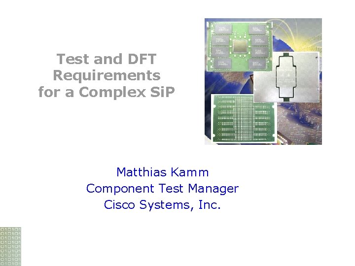
Test and DFT Requirements for a Complex Si. P Matthias Kamm Component Test Manager Cisco Systems, Inc.

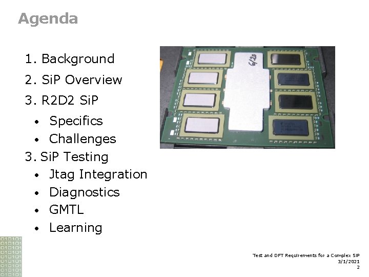
Agenda 1. Background 2. Si. P Overview 3. R 2 D 2 Si. P Specifics • Challenges 3. Si. P Testing • Jtag Integration • Diagnostics • GMTL • Learning • Test and DFT Requirements for a Complex Si. P 3/1/2021 2

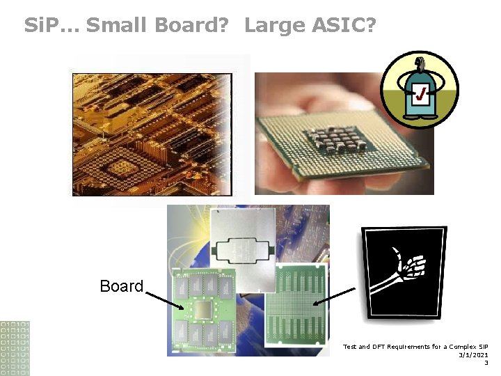
Si. P… Small Board? Large ASIC? Board ASIC Test and DFT Requirements for a Complex Si. P 3/1/2021 3

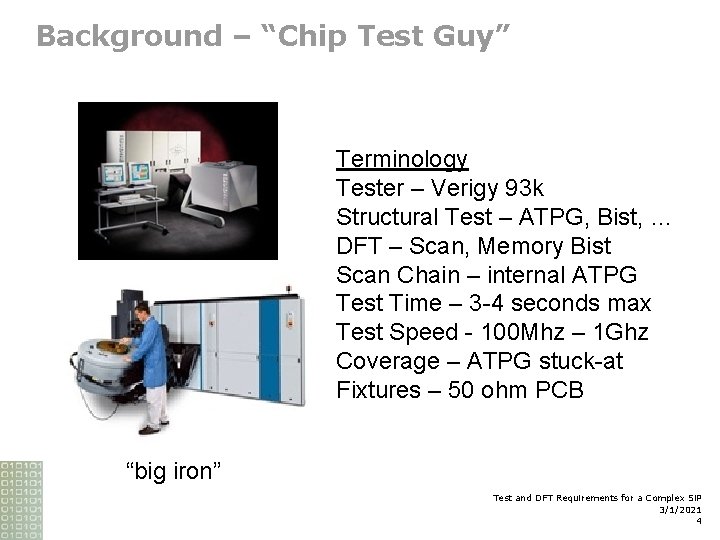
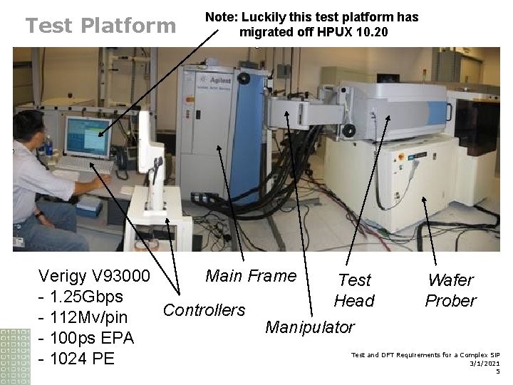
Background – “Chip Test Guy” Terminology Tester – Verigy 93 k Structural Test – ATPG, Bist, … DFT – Scan, Memory Bist Scan Chain – internal ATPG Test Time – 3 -4 seconds max Test Speed - 100 Mhz – 1 Ghz Coverage – ATPG stuck-at Fixtures – 50 ohm PCB “big iron” Test and DFT Requirements for a Complex Si. P 3/1/2021 4

Test Platform Note: Luckily this test platform has migrated off HPUX 10. 20 Verigy V 93000 Main Frame Test - 1. 25 Gbps Head Controllers - 112 Mv/pin Manipulator - 100 ps EPA - 1024 PE Wafer Prober Test and DFT Requirements for a Complex Si. P 3/1/2021 5

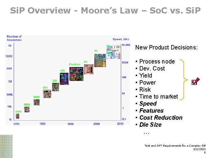
Si. P Overview - Moore’s Law – So. C vs. Si. P New Product Decisions: • Process node • Dev. Cost • Yield • Power • Risk • Time to market • Speed • Features • Cost Reduction • Die Size … Test and DFT Requirements for a Complex Si. P 3/1/2021 6

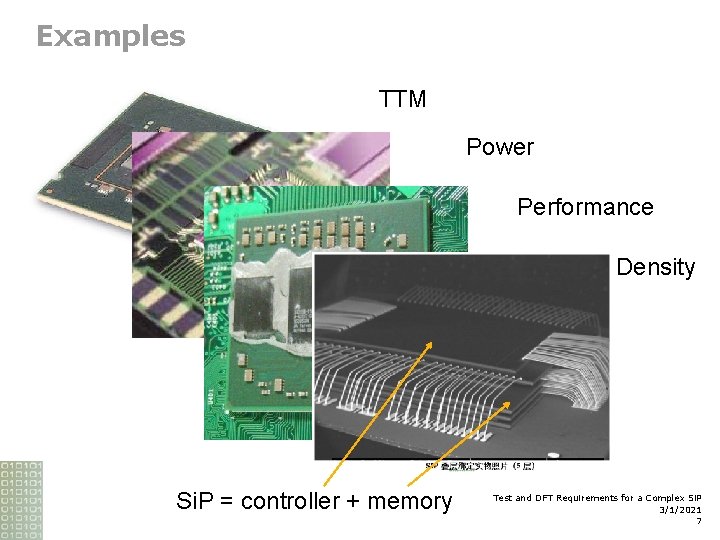
Examples TTM Power Performance Density Si. P = controller + memory Test and DFT Requirements for a Complex Si. P 3/1/2021 7

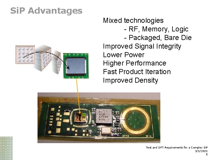
Si. P Advantages Mixed technologies - RF, Memory, Logic - Packaged, Bare Die Improved Signal Integrity Lower Power Higher Performance Fast Product Iteration Improved Density Test and DFT Requirements for a Complex Si. P 3/1/2021 8

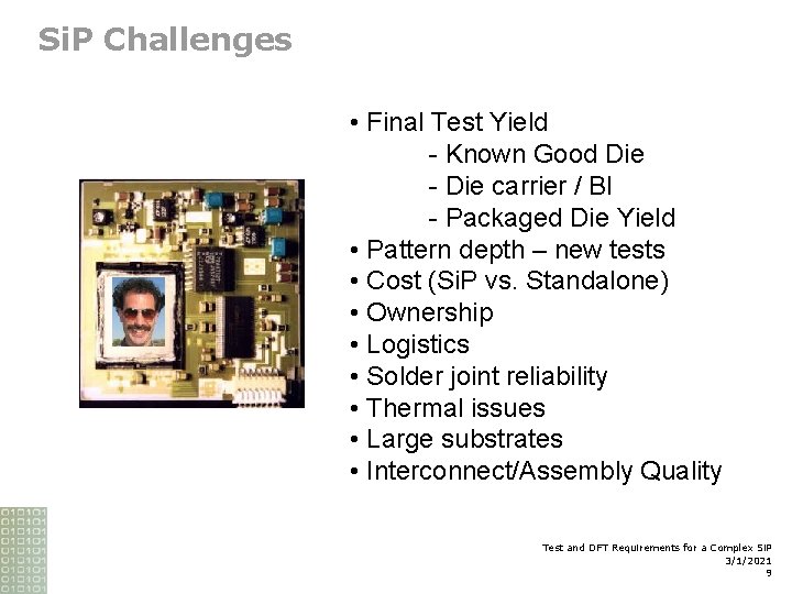
Si. P Challenges • Final Test Yield - Known Good Die - Die carrier / BI - Packaged Die Yield • Pattern depth – new tests • Cost (Si. P vs. Standalone) • Ownership • Logistics • Solder joint reliability • Thermal issues • Large substrates • Interconnect/Assembly Quality Test and DFT Requirements for a Complex Si. P 3/1/2021 9

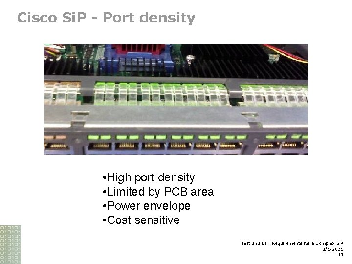
Cisco Si. P - Port density • High port density • Limited by PCB area • Power envelope • Cost sensitive Test and DFT Requirements for a Complex Si. P 3/1/2021 10

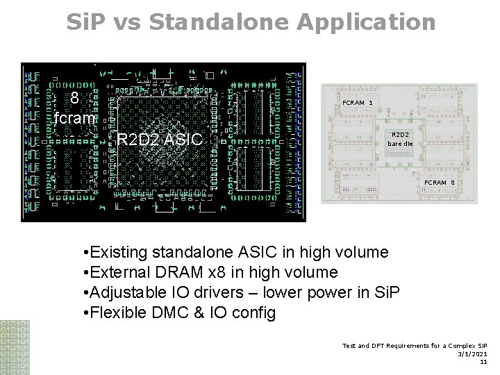
Si. P vs Standalone Application 8 fcram FCRAM 1 Module: R 2 D 2 ASIC Area: 3 signal layers 10 layers total no terminations 72 x 55 mm R 2 D 2 bare die FCRAM 8 • Existing standalone ASIC in high volume • External DRAM x 8 in high volume • Adjustable IO drivers – lower power in Si. P • Flexible DMC & IO config Test and DFT Requirements for a Complex Si. P 3/1/2021 11

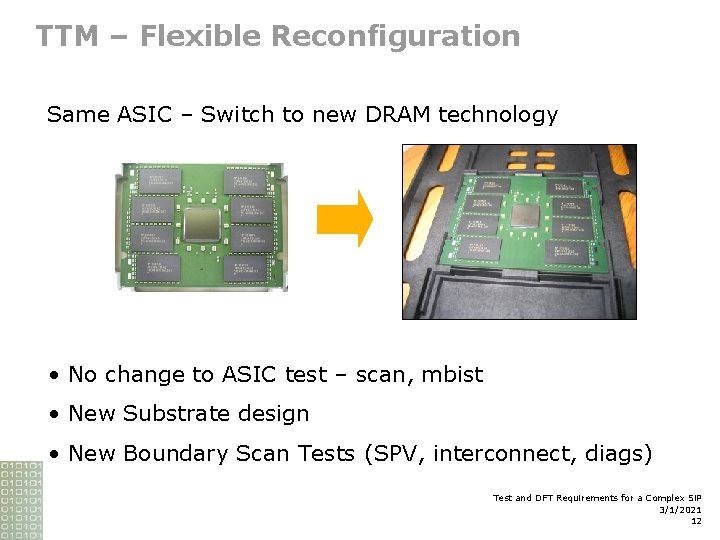
TTM – Flexible Reconfiguration Same ASIC – Switch to new DRAM technology • No change to ASIC test – scan, mbist • New Substrate design • New Boundary Scan Tests (SPV, interconnect, diags) Test and DFT Requirements for a Complex Si. P 3/1/2021 12

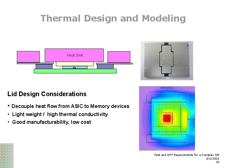
Thermal Design and Modeling Heat Sink die Lid Design Considerations • Decouple heat flow from ASIC to Memory devices • Light weight / high thermal conductivity • Good manufacturability, low cost Test and DFT Requirements for a Complex Si. P 3/1/2021 13

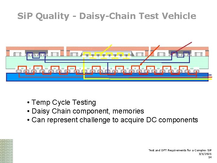
Si. P Quality - Daisy-Chain Test Vehicle L 1 L 3 L 2 • Temp Cycle Testing • Daisy Chain component, memories • Can represent challenge to acquire DC components Test and DFT Requirements for a Complex Si. P 3/1/2021 14

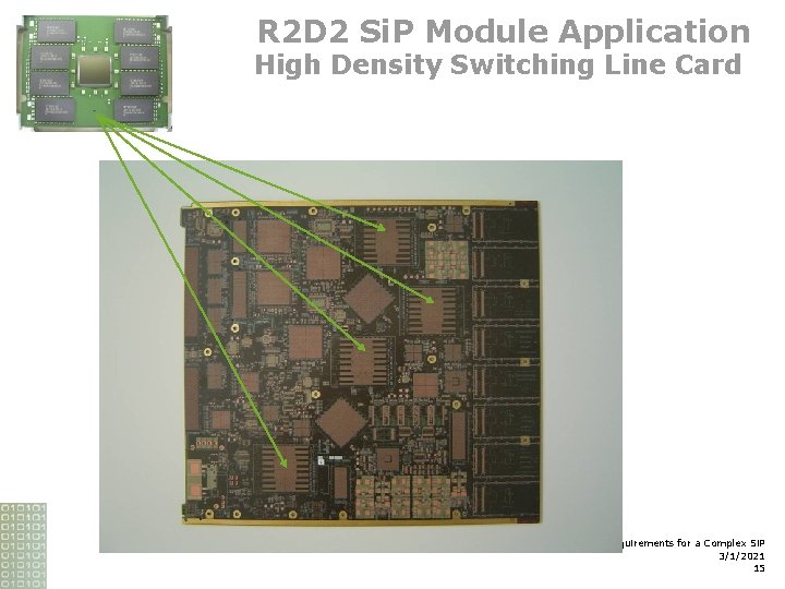
R 2 D 2 Si. P Module Application High Density Switching Line Card Test and DFT Requirements for a Complex Si. P 3/1/2021 15

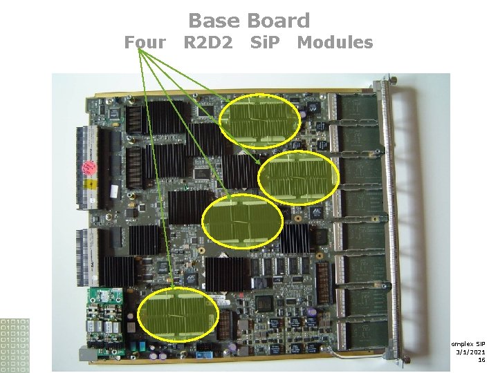
Four Base Board R 2 D 2 Si. P Modules Test and DFT Requirements for a Complex Si. P 3/1/2021 16

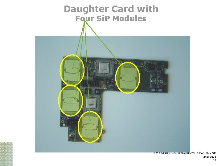
Daughter Card with Four Si. P Modules Test and DFT Requirements for a Complex Si. P 3/1/2021 17

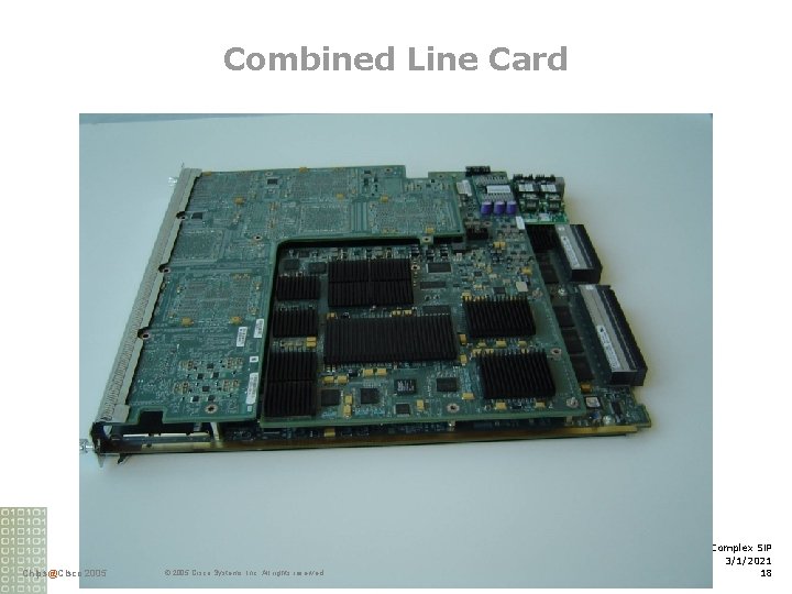
Combined Line Card Chips@Cisco 2005 © 2005 Cisco Systems, Inc. All rights reserved. Test and DFT Requirements for a Complex Si. P 3/1/2021 18

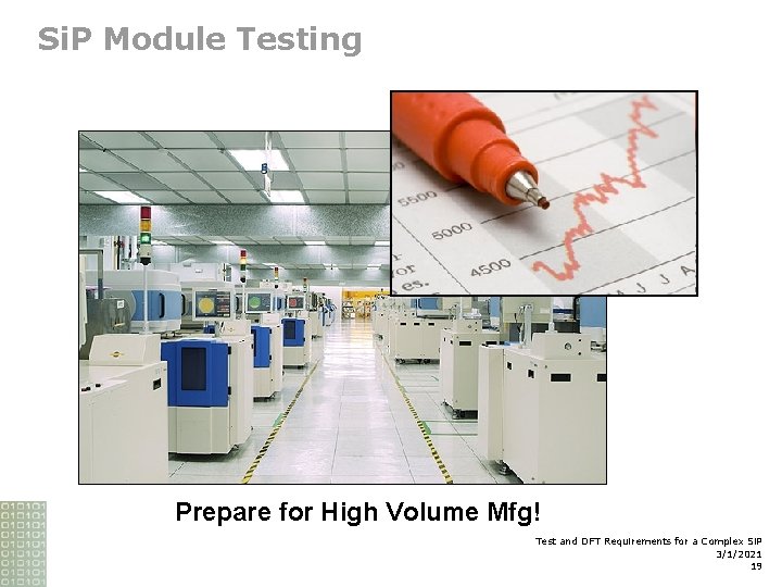
Si. P Module Testing Prepare for High Volume Mfg! Test and DFT Requirements for a Complex Si. P 3/1/2021 19

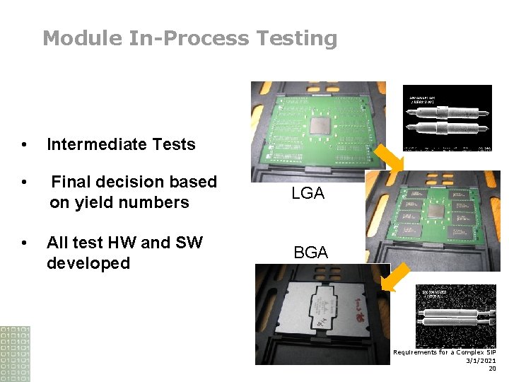
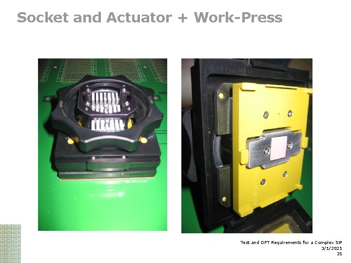
Module In-Process Testing • Intermediate Tests • Final decision based on yield numbers LGA • All test HW and SW developed BGA Test and DFT Requirements for a Complex Si. P 3/1/2021 20

Socket and Actuator + Work-Press Test and DFT Requirements for a Complex Si. P 3/1/2021 21

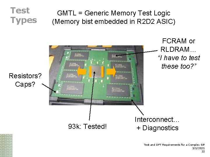
Test Types GMTL = Generic Memory Test Logic (Memory bist embedded in R 2 D 2 ASIC) FCRAM or RLDRAM… “I have to test these too? ” Resistors? Caps? 93 k: Tested! Interconnect… + Diagnostics Test and DFT Requirements for a Complex Si. P 3/1/2021 22

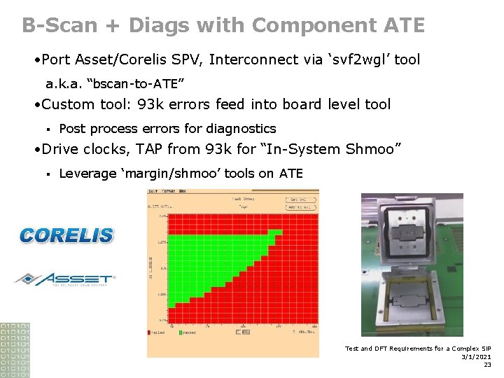
B-Scan + Diags with Component ATE • Port Asset/Corelis SPV, Interconnect via ‘svf 2 wgl’ tool a. k. a. “bscan-to-ATE” • Custom tool: 93 k errors feed into board level tool § Post process errors for diagnostics • Drive clocks, TAP from 93 k for “In-System Shmoo” § Leverage ‘margin/shmoo’ tools on ATE Test and DFT Requirements for a Complex Si. P 3/1/2021 23

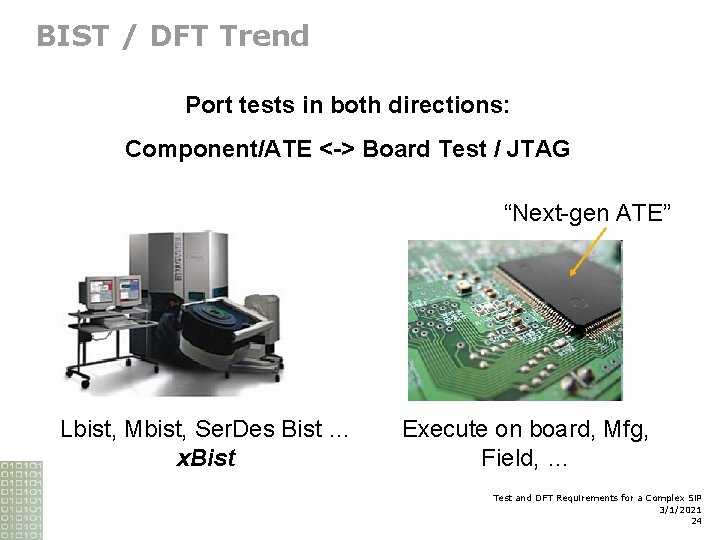
BIST / DFT Trend Port tests in both directions: Component/ATE <-> Board Test / JTAG “Next-gen ATE” Lbist, Mbist, Ser. Des Bist … x. Bist Execute on board, Mfg, Field, … Test and DFT Requirements for a Complex Si. P 3/1/2021 24

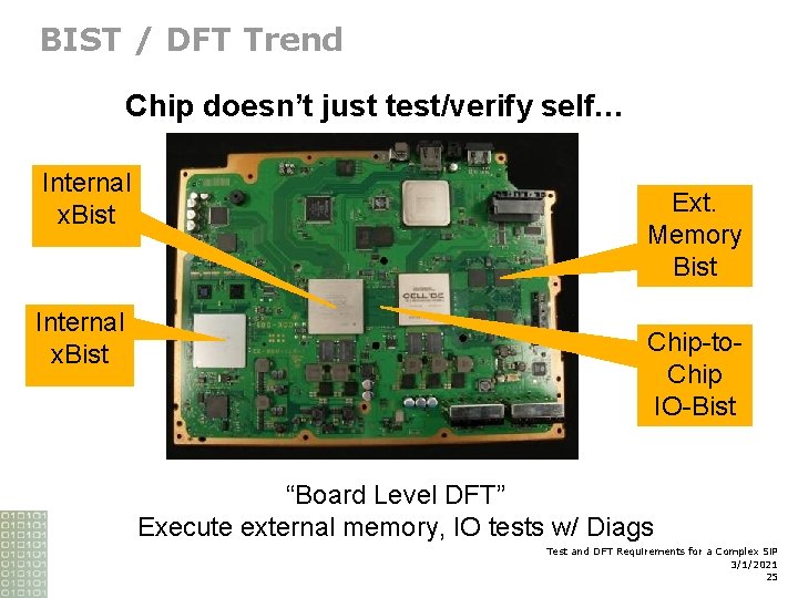
BIST / DFT Trend Chip doesn’t just test/verify self… Internal x. Bist Ext. Memory Bist Chip-to. Chip IO-Bist “Board Level DFT” Execute external memory, IO tests w/ Diags Test and DFT Requirements for a Complex Si. P 3/1/2021 25

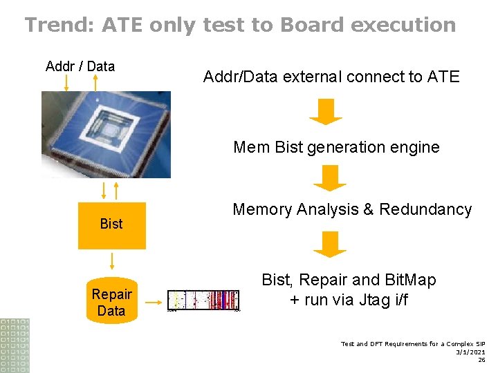
Trend: ATE only test to Board execution Addr / Data Addr/Data external connect to ATE Mem Bist generation engine Bist Repair Data Memory Analysis & Redundancy Bist, Repair and Bit. Map + run via Jtag i/f Test and DFT Requirements for a Complex Si. P 3/1/2021 26

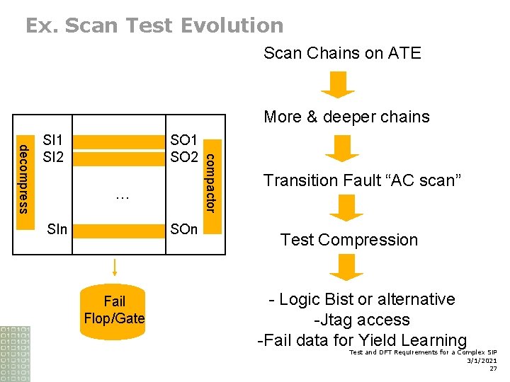
Ex. Scan Test Evolution Scan Chains on ATE More & deeper chains SO 1 SO 2 … SIn SOn Fail Flop/Gate compactor decompress SI 1 SI 2 Transition Fault “AC scan” Test Compression - Logic Bist or alternative -Jtag access -Fail data for Yield Learning Test and DFT Requirements for a Complex Si. P 3/1/2021 27

Si. P… Small Board? Large ASIC? Both! Test and DFT Requirements for a Complex Si. P 3/1/2021 28

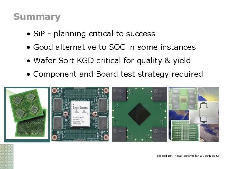
Summary • Si. P - planning critical to success • Good alternative to SOC in some instances • Wafer Sort KGD critical for quality & yield • Component and Board test strategy required Test and DFT Requirements for a Complex Si. P

Questions? matthias@cisco. com Test and DFT Requirements for a Complex Si. P 3/1/2021 30