TeraPixel APS for CALICE Progress meeting 6 th
![Diode Sum: Other Circuits Forked source follower [JC] Number of pmos Vdd Static current Diode Sum: Other Circuits Forked source follower [JC] Number of pmos Vdd Static current](https://slidetodoc.com/presentation_image/7bf18ecca15b9872b22803bd4976903e/image-10.jpg)
- Slides: 14

Tera-Pixel APS for CALICE Progress meeting, 6 th June 2006 Jamie Crooks, Microelectronics/RAL

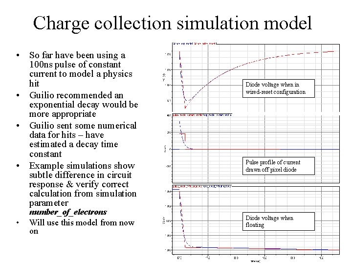
Charge collection simulation model • So far have been using a 100 ns pulse of constant current to model a physics hit • Guilio recommended an exponential decay would be more appropriate • Guilio sent some numerical data for hits – have estimated a decay time constant • Example simulations show subtle difference in circuit response & verify correct calculation from simulation parameter • number_of_electrons Will use this model from now on Diode voltage when in wired-reset configuration Pulse profile of current drawn off pixel diode Diode voltage when floating

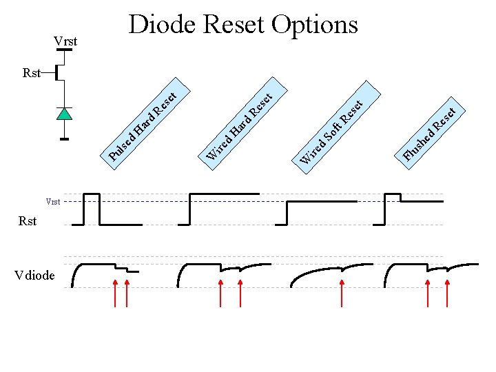
Vrst Rst Vdiode us Fl d t se t Re Re ft rd Ha d ar H So he d ire W lse d Pu Vrst Diode Reset Options Rst

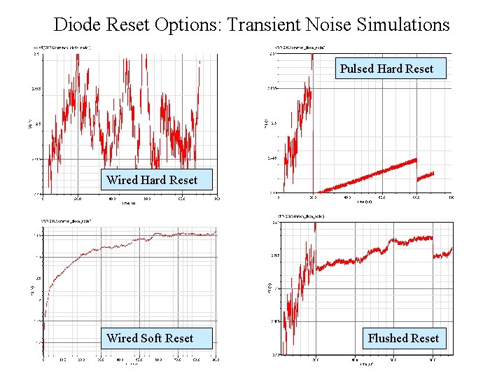
Diode Reset Options: Transient Noise Simulations Pulsed Hard Reset Wired Soft Reset Flushed Reset

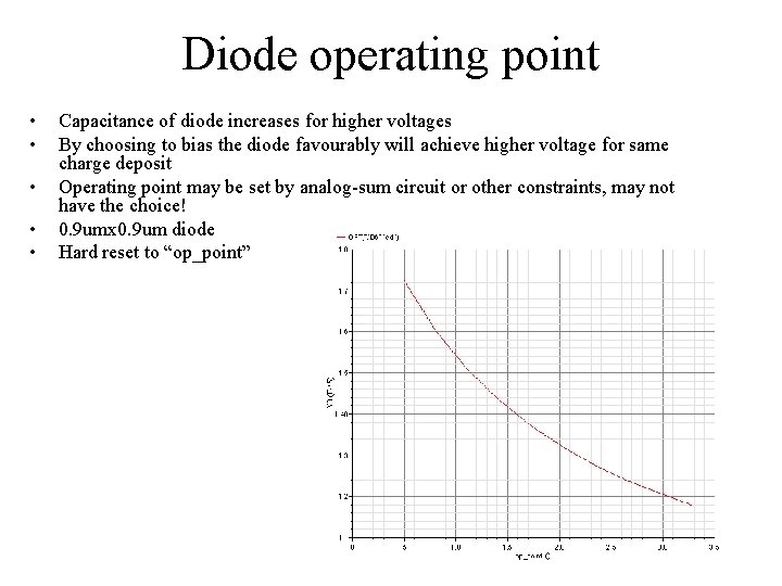
Diode operating point • • • Capacitance of diode increases for higher voltages By choosing to bias the diode favourably will achieve higher voltage for same charge deposit Operating point may be set by analog-sum circuit or other constraints, may not have the choice! 0. 9 umx 0. 9 um diode Hard reset to “op_point”

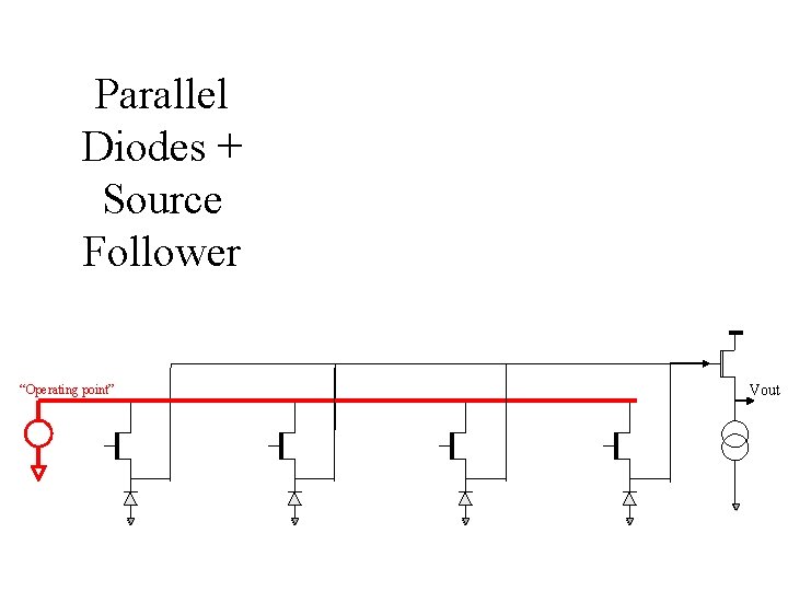
Parallel Diodes + Source Follower “Operating point” Vout

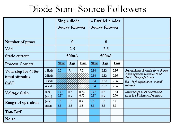
Diode Sum: Source Followers Single diode Source follower 4 Parallel diodes Source follower 0 0 2. 5 500 n. A Number of pmos Vdd Static current Slow Typ Fast Slow Typ 8. 0 7. 4 7. 0 2. 34 2. 32 2. 36 2 diode 2. 34 2. 32 2. 36 3 diode 2. 34 2. 32 2. 36 4 diode 2. 34 2. 32 2. 36 Expect identical results since charge summing node is common to all diodes: The perfect sum! But – high capacitance small voltages Lower range could be achieved using low Vt devices if required Process Corners Fast Vout step for 450 einput stimulus (m. V) 1 diode Voltage Gain (min) (max) 0. 77 0. 87 0. 8 0. 9 0. 84 0. 90 Range of operation (min) (max) 1. 0 3. 3 0. 8 3. 3 Ton/Toff Noise

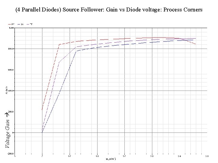
Voltage Gain (4 Parallel Diodes) Source Follower: Gain vs Diode voltage: Process Corners

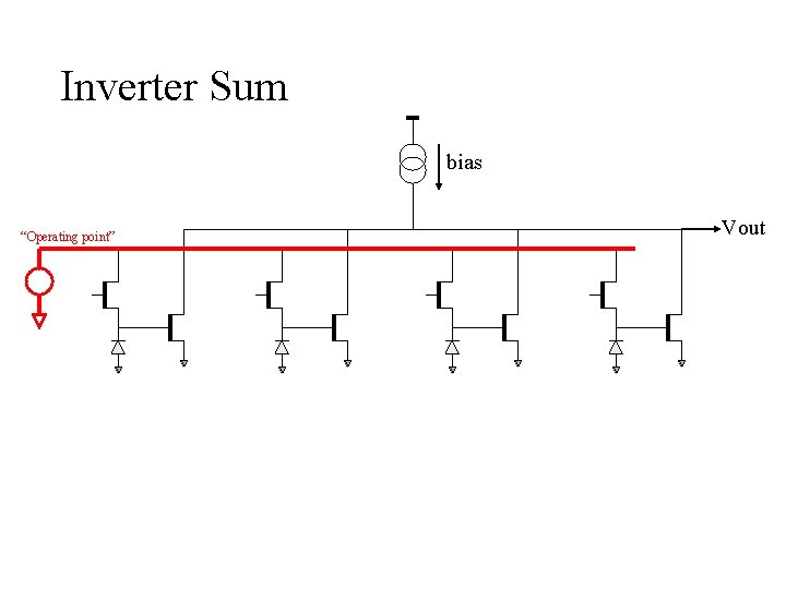
Inverter Sum bias “Operating point” Vout
![Diode Sum Other Circuits Forked source follower JC Number of pmos Vdd Static current Diode Sum: Other Circuits Forked source follower [JC] Number of pmos Vdd Static current](https://slidetodoc.com/presentation_image/7bf18ecca15b9872b22803bd4976903e/image-10.jpg)
Diode Sum: Other Circuits Forked source follower [JC] Number of pmos Vdd Static current Process Corners Inverter sum [RT] 0 1 2. 5 500 n. A Slow Typ Fast Vout step for 450 einput stimulus (m. V) 1 diode 4. 23 4. 40 2 diode 4. 68 4. 77 3 diode 4. 84 4. 90 4 diode 4. 92 5. 0 4. 97 Voltage Gain (min) (max) 0. 185 0. 244 0. 190 0. 252 0. 196 0. 255 Range of operation (min) (max) Nmos amplifier [Dorokhov/mimosa 15] 0 <3 u. A Not current limited!

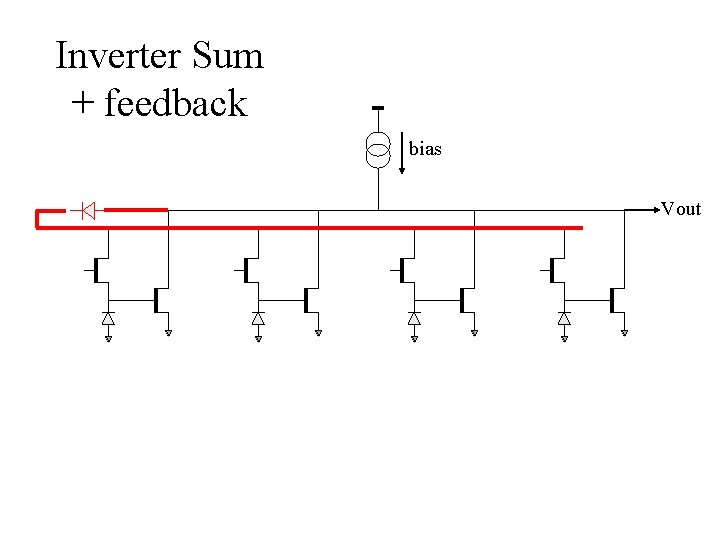
Inverter Sum + feedback bias Vout

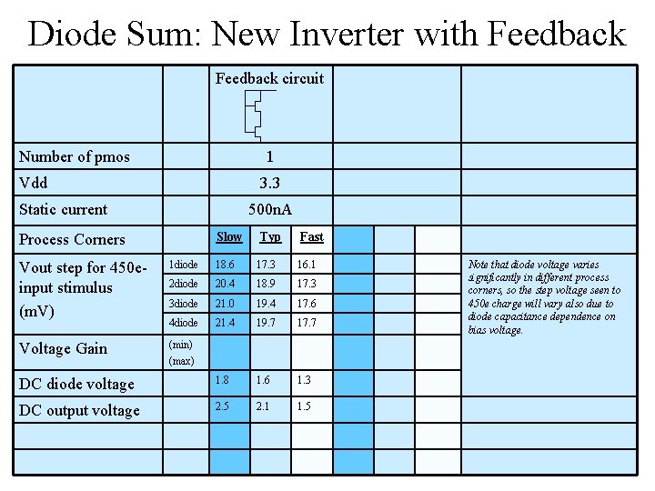
Diode Sum: New Inverter with Feedback circuit Number of pmos 1 Vdd 3. 3 Static current 500 n. A Process Corners Slow Typ Fast Vout step for 450 einput stimulus (m. V) 1 diode 18. 6 17. 3 16. 1 2 diode 20. 4 18. 9 17. 3 3 diode 21. 0 19. 4 17. 6 4 diode 21. 4 19. 7 17. 7 Voltage Gain (min) (max) DC diode voltage 1. 8 1. 6 1. 3 DC output voltage 2. 5 2. 1 1. 5 Note that diode voltage varies significantly in different process corners, so the step voltage seen to 450 e charge will vary also due to diode capacitance dependence on bias voltage.

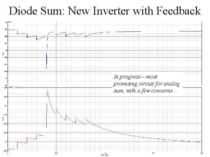
Diode Sum: New Inverter with Feedback In progress – most promising circuit for analog sum, with a few concerns…

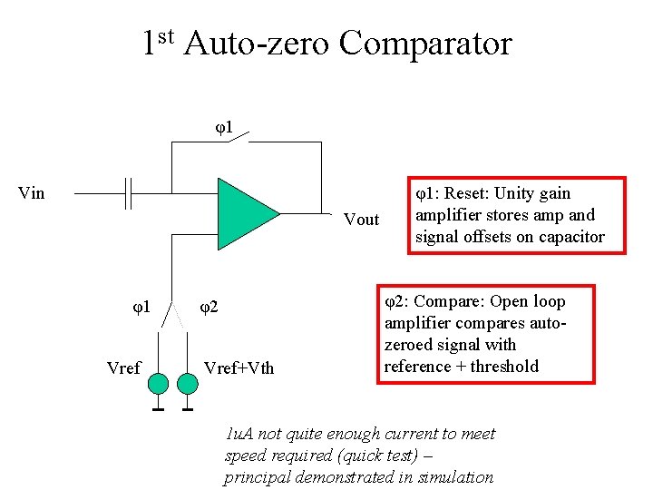
1 st Auto-zero Comparator φ1 Vin Vout φ1 Vref φ2 Vref+Vth φ1: Reset: Unity gain amplifier stores amp and signal offsets on capacitor φ2: Compare: Open loop amplifier compares autozeroed signal with reference + threshold 1 u. A not quite enough current to meet speed required (quick test) – principal demonstrated in simulation