
Technische Universitt Berlin Microwave Engineering Design of Microwave
Technische Universität Berlin Microwave Engineering Design of Microwave Power Amplifier with ADS Technische Universität Berlin Fachgebiet Mikrowellentechnik Daniel Gruner, Ahmed Sayed, Ahmed Al Tanany, Khaled Bathich, Henrique Portela, Amin Hamidian, Georg Boeck Gruner, ADS User Meeting 09 1
Technische Universität Berlin Microwave Engineering Outline • Introduction • PA Overview • ADS Design Flow • Power Amplifier Design Transistor Characterization Hybrid Broadband Power Amplifier Hybrid Doherty Power Amplifier Hybrid Switch Mode Power Amplifier Monolithic 6 GHz Power Amplifier Monolithic 24 / 60 GHz Power Amplifier • Summary and Conclusion Gruner, ADS User Meeting 09 2
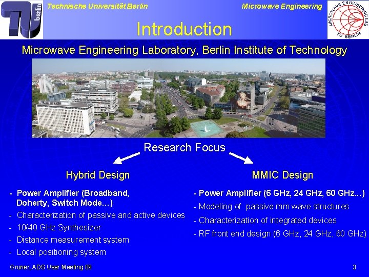
Technische Universität Berlin Microwave Engineering Introduction Microwave Engineering Laboratory, Berlin Institute of Technology Research Focus Hybrid Design - Power Amplifier (Broadband, Doherty, Switch Mode…) - Characterization of passive and active devices - 10/40 GHz Synthesizer - Distance measurement system - Local positioning system Gruner, ADS User Meeting 09 MMIC Design - Power Amplifier (6 GHz, 24 GHz, 60 GHz…) - Modeling of passive mm wave structures - Characterization of integrated devices - RF front end design (6 GHz, 24 GHz, 60 GHz) 3
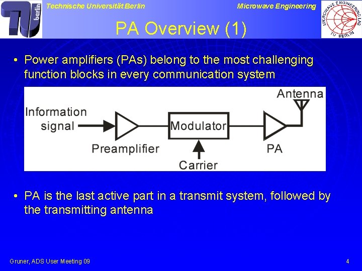
Technische Universität Berlin Microwave Engineering PA Overview (1) • Power amplifiers (PAs) belong to the most challenging function blocks in every communication system • PA is the last active part in a transmit system, followed by the transmitting antenna Gruner, ADS User Meeting 09 4
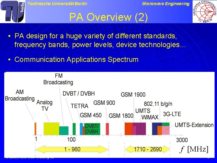
Technische Universität Berlin Microwave Engineering PA Overview (2) • PA design for a huge variety of different standards, frequency bands, power levels, device technologies… • Communication Applications Spectrum f [MHz] Gruner, ADS User Meeting 09 5
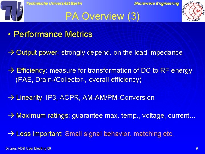
Technische Universität Berlin Microwave Engineering PA Overview (3) • Performance Metrics Output power: strongly depend. on the load impedance Efficiency: measure for transformation of DC to RF energy (PAE, Drain-/Collector-, overall efficiency) Linearity: IP 3, ACPR, AM-AM/PM-Conversion Maximum ratings: guarantee max. temp. , voltage, current… Less important: Small signal behavior, matching etc. Gruner, ADS User Meeting 09 6

Technische Universität Berlin Microwave Engineering PA Overview (4) • Fundamental PA categories Linear PA - Classes A, B, AB, C Switch Mode PA - Classes D, D-1, E, F, F-1, S, etc. Combinations, extensions, smart transmitters - Power Combining, Doherty, Chireix, LINC, etc. Gruner, ADS User Meeting 09 7
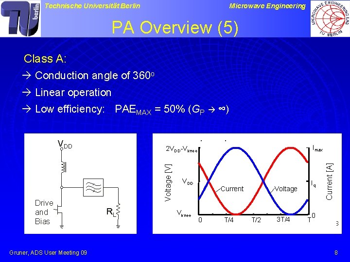
Technische Universität Berlin Microwave Engineering PA Overview (5) Class A: Conduction angle of 360 o Linear operation Low efficiency: PAEMAX = 50% (GP ∞) Gruner, ADS User Meeting 09 Voltage [V] Drive and Bias I 2 VDD-Vknee DS RL Vp VDD Vknee IDS Load line Imax Bias point I Imax. Current /2 0 VGST/4 0 Current [A] VDD q Voltage T/2 3 T/4 VDD T 0 VDS 8
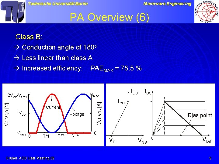
Technische Universität Berlin Microwave Engineering PA Overview (6) Class B: Conduction angle of 180 o Less linear than class A Increased efficiency: PAEMAX = 78. 5 % VDD Voltage T/4 Gruner, ADS User Meeting 09 T/2 3 T/4 T IDS Imax Current [A] Voltage [V] Current Vknee 0 IDS Imax 2 VDD-Vknee Bias point 0 VP VGS 0 VDS 9
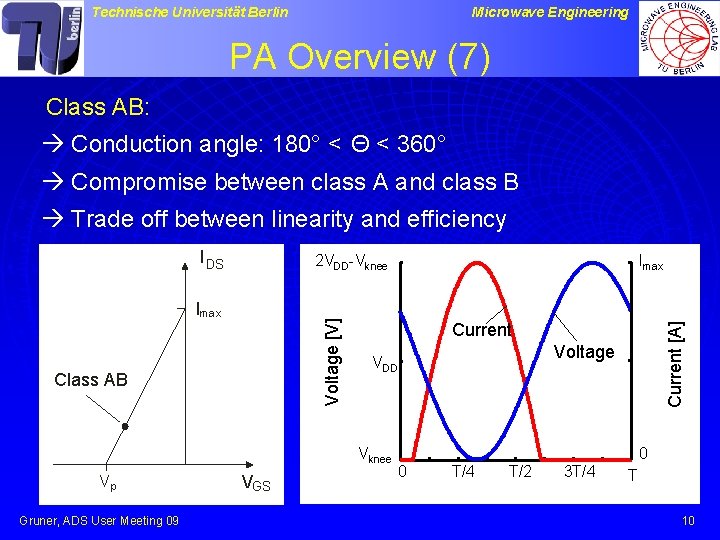
Technische Universität Berlin Microwave Engineering PA Overview (7) Class AB: Conduction angle: 180° < Θ < 360° Compromise between class A and class B Trade off between linearity and efficiency 2 VDD-Vknee Voltage [V] Imax Class AB Gruner, ADS User Meeting 09 VGS Imax Current Voltage VDD Vknee Vp Current [A] I DS 0 0 T/4 T/2 3 T/4 T 10
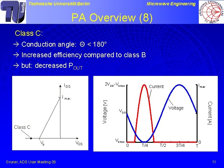
Technische Universität Berlin Microwave Engineering PA Overview (8) Class C: Conduction angle: Θ < 180° Increased efficiency compared to class B but: decreased POUT 2 VDD-Vknee I DS Imax Current [A] Voltage [V] I max Voltage VDD Class C Vp Gruner, ADS User Meeting 09 VGS Vknee 0 T/4 T/2 3 T/4 T 0 11
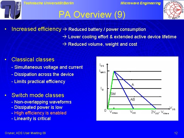
Technische Universität Berlin Microwave Engineering PA Overview (9) • Increased efficiency Reduced battery / power consumption Lower cooling effort & extended active device lifetime Reduced volume, weight and cost • Classical classes - Simultaneous voltage and current - Dissipation across the device IDS IMAX - Limits practical efficiency A IQ • Switch mode classes - Non-overlapping waveforms - Dissipated power is low - High efficiency is enabled - Linearity is critical Gruner, ADS User Meeting 09 SM AB 0 V Knee VDD 2 VDD- VKnee VDS 12
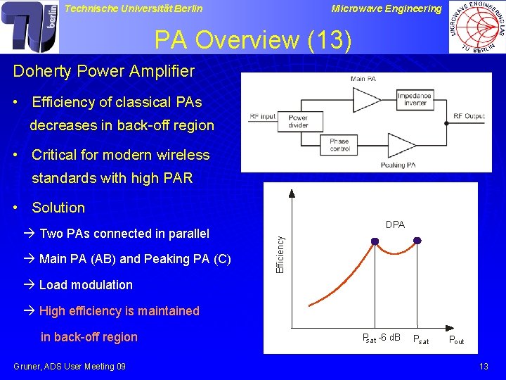
Technische Universität Berlin Microwave Engineering PA Overview (13) Doherty Power Amplifier • Efficiency of classical PAs decreases in back-off region • Critical for modern wireless standards with high PAR • Solution Main PA (AB) and Peaking PA (C) Efficiency Two PAs connected in parallel DPA Load modulation High efficiency is maintained in back-off region Gruner, ADS User Meeting 09 P -6 d. B sat Pout 13
P S ct a a R S ni edssci m u m d i ul D v e a el R e C sas t ti Si o gi t gnor nun c t u r e s art Technische Universität Berlin Microwave Engineering ADS Design Flow Gruner, ADS User Meeting 09 14
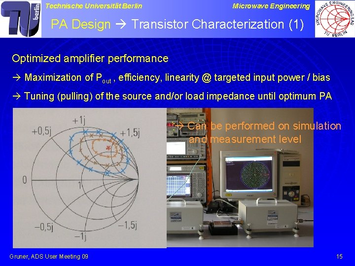
Technische Universität Berlin Microwave Engineering PA Design Transistor Characterization (1) Optimized amplifier performance Maximization of Pout , efficiency, linearity @ targeted input power / bias Tuning (pulling) of the source and/or load impedance until optimum PA Can be performed on simulation and measurement level Gruner, ADS User Meeting 09 15
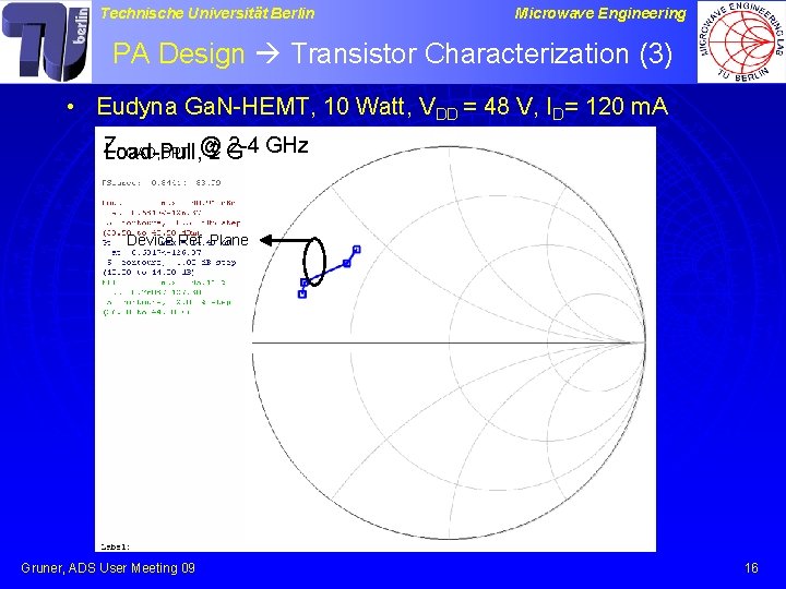
Technische Universität Berlin Microwave Engineering PA Design Transistor Characterization (3) • Eudyna Ga. N-HEMT, 10 Watt, VDD = 48 V, ID= 120 m. A Z LOAD, OPT @ 2 -4 GHz Load-Pull, 2 GHz Device Ref. Plane Gruner, ADS User Meeting 09 16
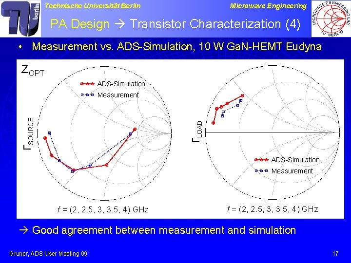
Technische Universität Berlin Microwave Engineering PA Design Transistor Characterization (4) • Measurement vs. ADS-Simulation, 10 W Ga. N-HEMT Eudyna ZOPT ADS-Simulation ΓLOAD ΓSOURCE Measurement ADS-Simulation Measurement f = (2, 2. 5, 3, 3. 5, 4) GHz Good agreement between measurement and simulation Gruner, ADS User Meeting 09 17
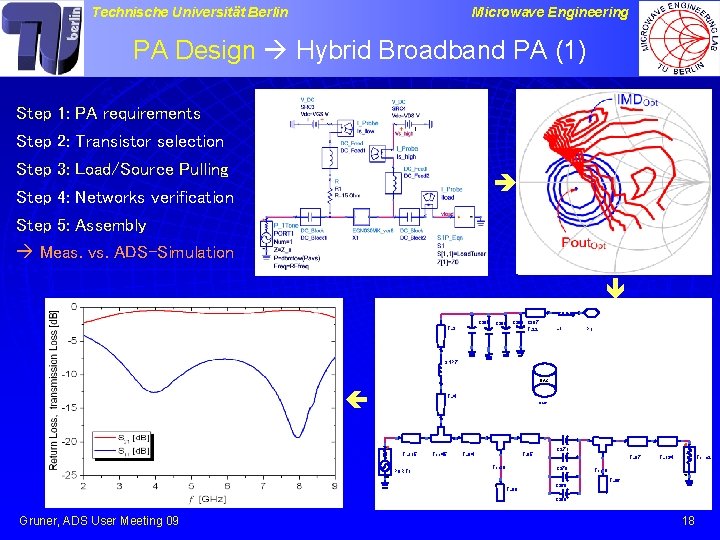
Technische Universität Berlin Microwave Engineering PA Design Hybrid Broadband PA (1) Step 1: PA requirements Step 2: Transistor selection Step 3: Load/Source Pulling Step 4: Networks verification Step 5: Assembly Meas. vs. ADS-Simulation Pout contours C 305 TL 3 C 306 C 308 C 307 TL 22 L 1 P 1 SNP 7 DAC TL 4 DAC 1 TL 115 PORT 1 Tee 45 TL 94 TL 95 Tee 39 C 271 TL 97 C 270 TL 98 C 269 Term 2 TL 134 Tee 38 TL 96 C 298 Gruner, ADS User Meeting 09 18
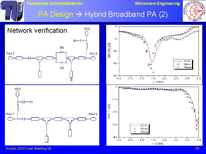
Technische Universität Berlin Microwave Engineering PA Design Hybrid Broadband PA (2) Network verification Gruner, ADS User Meeting 09 19
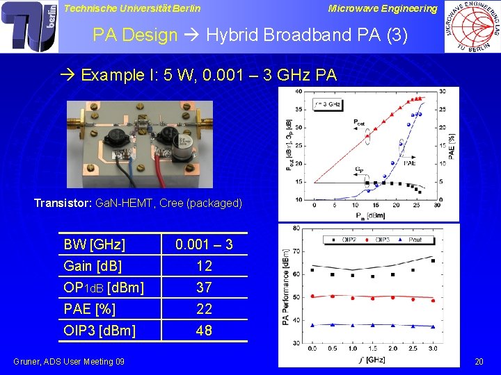
Technische Universität Berlin Microwave Engineering PA Design Hybrid Broadband PA (3) Example I: 5 W, 0. 001 – 3 GHz PA Transistor: Ga. N-HEMT, Cree (packaged) BW [GHz] 0. 001 – 3 Gain [d. B] 12 OP 1 d. B [d. Bm] 37 PAE [%] 22 OIP 3 [d. Bm] 48 Gruner, ADS User Meeting 09 20
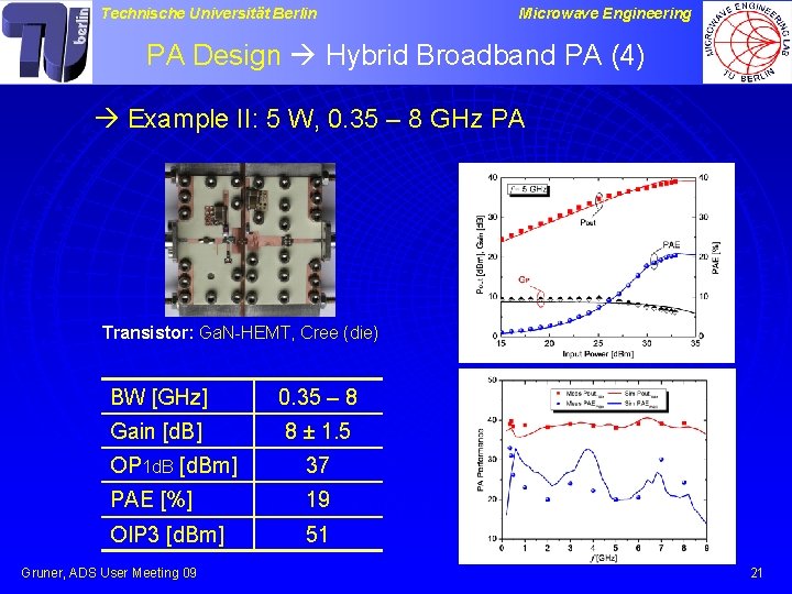
Technische Universität Berlin Microwave Engineering PA Design Hybrid Broadband PA (4) Example II: 5 W, 0. 35 – 8 GHz PA Transistor: Ga. N-HEMT, Cree (die) BW [GHz] 0. 35 – 8 Gain [d. B] 8 ± 1. 5 OP 1 d. B [d. Bm] 37 PAE [%] 19 OIP 3 [d. Bm] 51 Gruner, ADS User Meeting 09 21
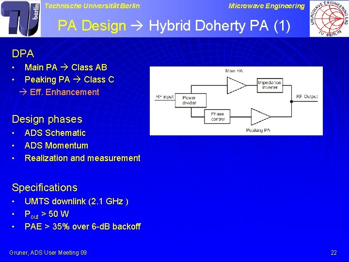
Technische Universität Berlin Microwave Engineering PA Design Hybrid Doherty PA (1) DPA • Main PA Class AB • Peaking PA Class C Eff. Enhancement Design phases • • • ADS Schematic ADS Momentum Realization and measurement Specifications • • • UMTS downlink (2. 1 GHz ) Pout > 50 W PAE > 35% over 6 -d. B backoff Gruner, ADS User Meeting 09 22
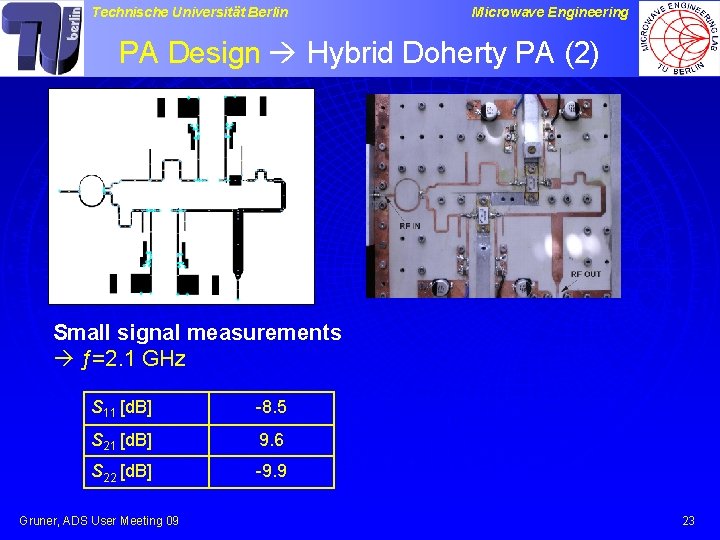
Technische Universität Berlin Microwave Engineering PA Design Hybrid Doherty PA (2) Small signal measurements ƒ=2. 1 GHz S 11 [d. B] -8. 5 S 21 [d. B] 9. 6 S 22 [d. B] -9. 9 Gruner, ADS User Meeting 09 23
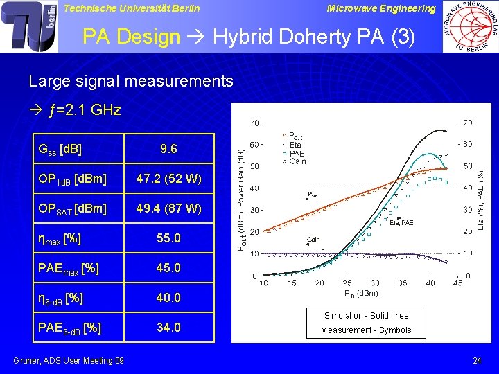
Technische Universität Berlin Microwave Engineering PA Design Hybrid Doherty PA (3) Large signal measurements ƒ=2. 1 GHz Gss [d. B] 9. 6 OP 1 d. B [d. Bm] 47. 2 (52 W) OPSAT [d. Bm] 49. 4 (87 W) ηmax [%] 55. 0 PAEmax [%] 45. 0 η 6 -d. B [%] 40. 0 Simulation - Solid lines PAE 6 -d. B [%] Gruner, ADS User Meeting 09 34. 0 Measurement - Symbols 24
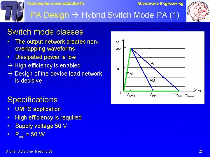
Technische Universität Berlin Microwave Engineering PA Design Hybrid Switch Mode PA (1) Switch mode classes • The output network creates nonoverlapping waveforms • Dissipated power is low High efficiency is enabled Design of the device load network is decisive Specifications • • IDS IMAX A IQ SM AB 0 V Knee VDD 2 VDD- VKnee VDS UMTS application High efficiency is required Supply voltage 50 V Pout = 50 W Gruner, ADS User Meeting 09 25
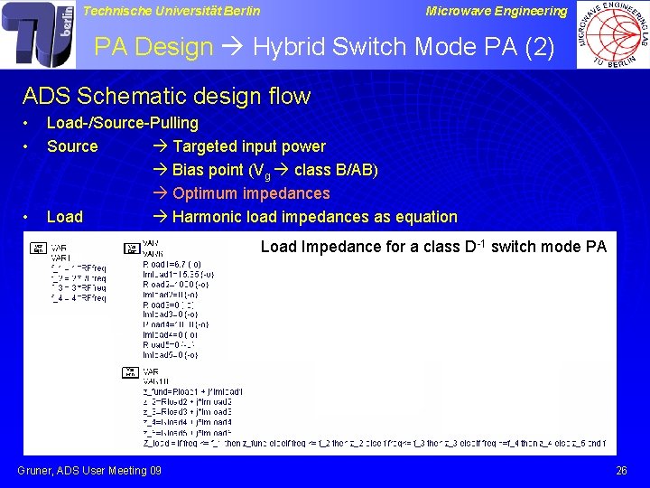
Technische Universität Berlin Microwave Engineering PA Design Hybrid Switch Mode PA (2) ADS Schematic design flow • • • Load-/Source-Pulling Source Targeted input power Bias point (Vg class B/AB) Optimum impedances Load Harmonic load impedances as equation Load Impedance for a class D-1 switch mode PA Gruner, ADS User Meeting 09 26
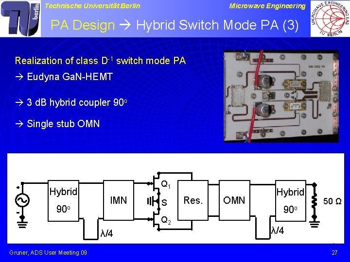
Technische Universität Berlin Microwave Engineering PA Design Hybrid Switch Mode PA (3) Realization of class D-1 switch mode PA Eudyna Ga. N-HEMT 3 d. B hybrid coupler 90 o Single stub OMN Hybrid 90 o Q 1 IMN S S Q 2 λ/4 Gruner, ADS User Meeting 09 S Res. OMN Hybrid 90 o R 50 Ω λ/4 27
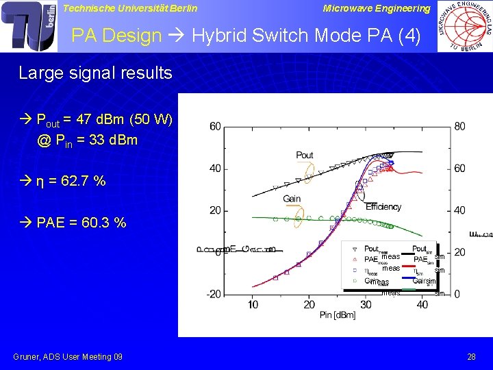
Technische Universität Berlin Microwave Engineering PA Design Hybrid Switch Mode PA (4) Large signal results Pout = 47 d. Bm (50 W) @ Pin = 33 d. Bm η = 62. 7 % PAE = 60. 3 % meas sim meas Gruner, ADS User Meeting 09 sim 28

Technische Universität Berlin Microwave Engineering PA Design Monolithic 6 GHz PA (1) Development of a fully integrated 6 GHz PA • Applications 6 GHz Wireless LAN Vehicular environments (IEEE P 802. 11 p) • Linear power amplifier Class AB operation Push-Pull topology Low supply voltage Si. Ge HBT technology Gruner, ADS User Meeting 09 29
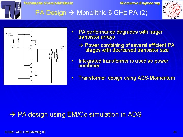
Technische Universität Berlin Microwave Engineering PA Design Monolithic 6 GHz PA (2) • PA performance degrades with larger transistor arrays Power combining of several efficient PA stages with decreased transistor size • Integrated transformer is used as power combiner • Transformer design using ADS-Momentum PA design using EM/Co simulation in ADS Gruner, ADS User Meeting 09 30
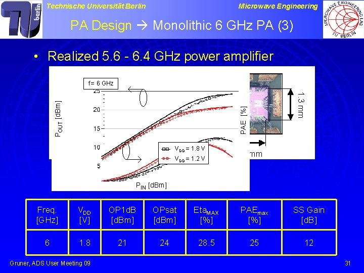
Technische Universität Berlin Microwave Engineering PA Design Monolithic 6 GHz PA (3) • Realized 5. 6 - 6. 4 GHz power amplifier PAE [%] 1. 3 mm POUT [d. Bm] f = 6 GHz VDD = 1. 8 V VDD = 1. 2 V 1. 6 mm PIN [d. Bm] Freq. [GHz] VDD [V] OP 1 d. B [d. Bm] OPsat [d. Bm] Eta. MAX [%] PAEmax [%] SS Gain [d. B] 6 1. 8 21 24 28. 5 25 12 Gruner, ADS User Meeting 09 31

Technische Universität Berlin Microwave Engineering PA Design Monolithic 24 / 60 GHz PA (1) • 24 GHz ISM band Industrial, scientific and medical applications • Targets Gain > 13. 5 d. B OP 1 d. B > 11 d. Bm PAE > 15 % Gruner, ADS User Meeting 09 32
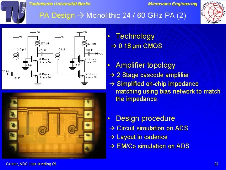
Technische Universität Berlin Microwave Engineering PA Design Monolithic 24 / 60 GHz PA (2) • Technology 0. 18 μm CMOS Vbias RFin • Amplifier topology 2 Stage cascode amplifier Simplified on-chip impedance matching using bias network to match the impedance. • Design procedure Circuit simulation on ADS Layout in cadence EM/Co simulation on ADS Gruner, ADS User Meeting 09 33
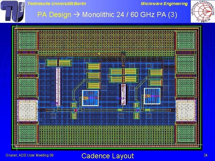
Technische Universität Berlin Microwave Engineering PA Design Monolithic 24 / 60 GHz PA (3) Gruner, ADS User Meeting 09 Cadence Layout 34
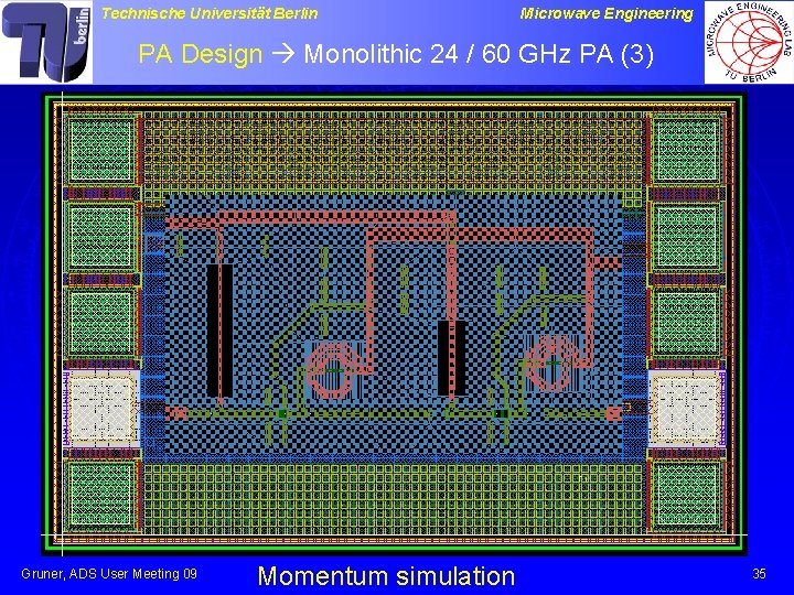
Technische Universität Berlin Microwave Engineering PA Design Monolithic 24 / 60 GHz PA (3) Gruner, ADS User Meeting 09 Momentum simulation 35
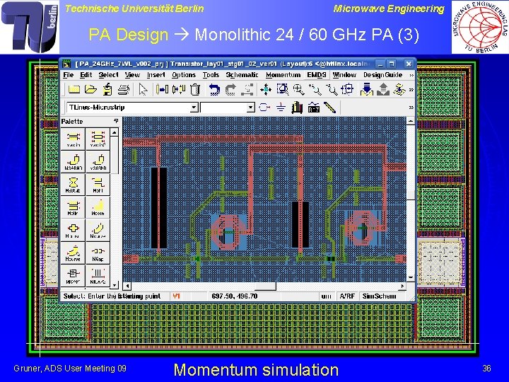
Technische Universität Berlin Microwave Engineering PA Design Monolithic 24 / 60 GHz PA (3) Gruner, ADS User Meeting 09 Momentum simulation 36
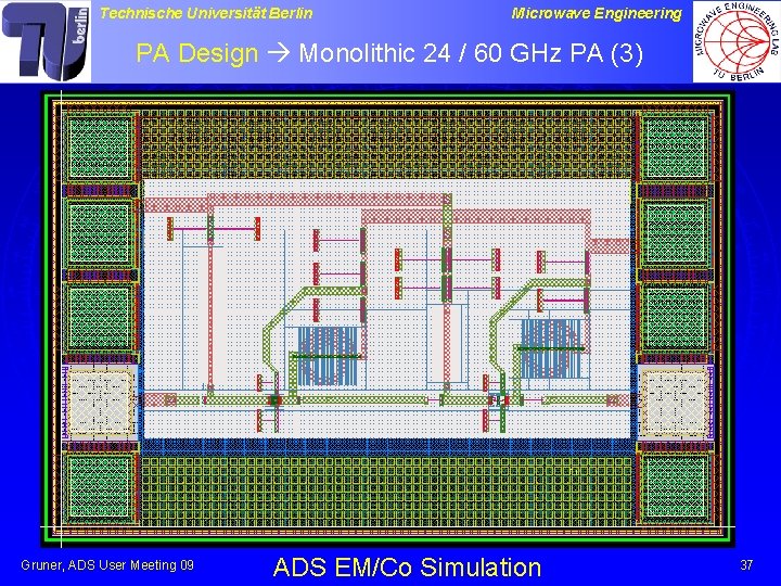
Technische Universität Berlin Microwave Engineering PA Design Monolithic 24 / 60 GHz PA (3) Gruner, ADS User Meeting 09 ADS EM/Co Simulation 37
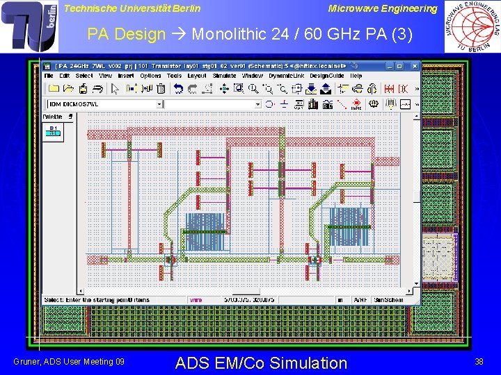
Technische Universität Berlin Microwave Engineering PA Design Monolithic 24 / 60 GHz PA (3) Gruner, ADS User Meeting 09 ADS EM/Co Simulation 38
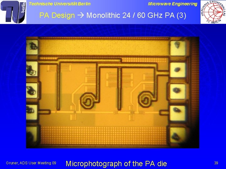
Technische Universität Berlin Microwave Engineering PA Design Monolithic 24 / 60 GHz PA (3) Gruner, ADS User Meeting 09 Microphotograph of the PA die 39
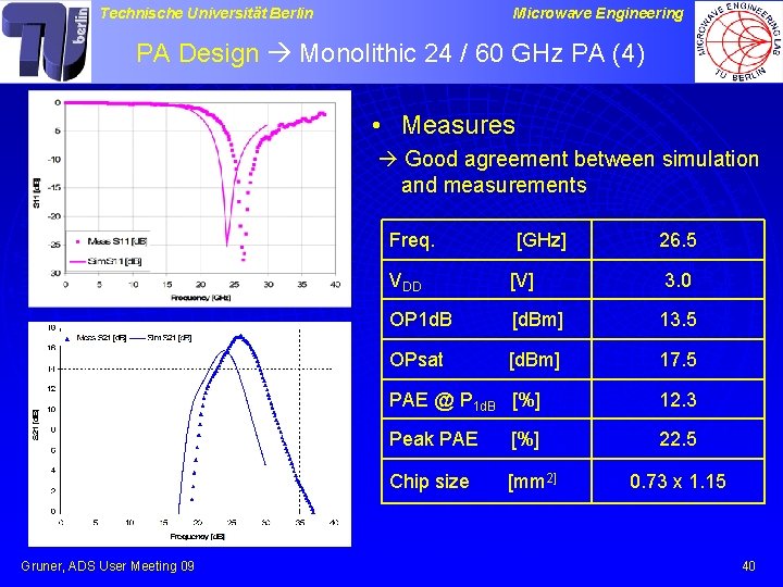
Technische Universität Berlin Microwave Engineering PA Design Monolithic 24 / 60 GHz PA (4) • Measures Good agreement between simulation and measurements Freq. [GHz] 26. 5 VDD [V] 3. 0 OP 1 d. B [d. Bm] 13. 5 OPsat [d. Bm] 17. 5 PAE @ P 1 d. B [%] 12. 3 Peak PAE [%] 22. 5 Chip size [mm 2] Gruner, ADS User Meeting 09 0. 73 x 1. 15 40
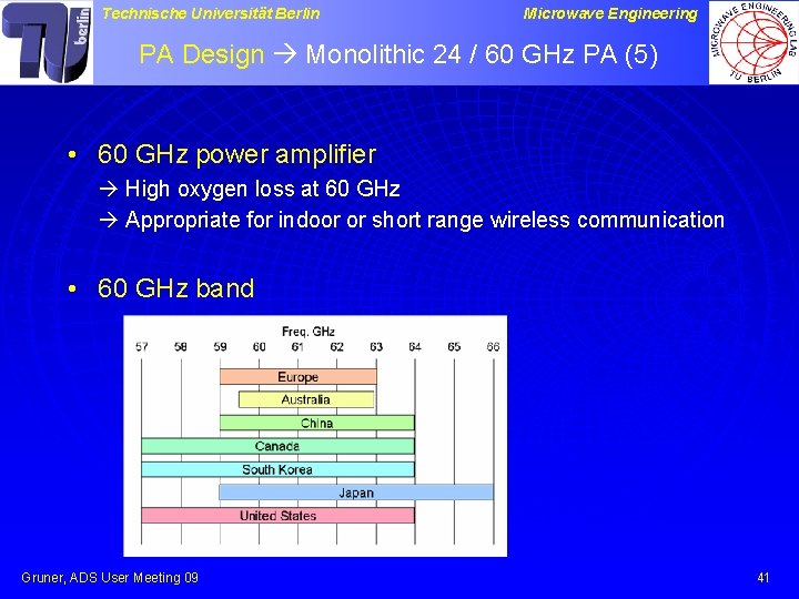
Technische Universität Berlin Microwave Engineering PA Design Monolithic 24 / 60 GHz PA (5) • 60 GHz power amplifier High oxygen loss at 60 GHz Appropriate for indoor or short range wireless communication • 60 GHz band Gruner, ADS User Meeting 09 41
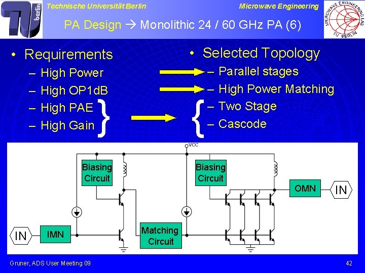
Technische Universität Berlin Microwave Engineering PA Design Monolithic 24 / 60 GHz PA (6) • Selected Topology • Requirements High Power High OP 1 d. B High PAE High Gain } } – – Biasing Circuit – – Parallel stages High Power Matching Two Stage Cascode Biasing Circuit OMN IN IMN Gruner, ADS User Meeting 09 IN Matching Circuit 42
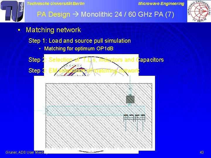
Technische Universität Berlin Microwave Engineering PA Design Monolithic 24 / 60 GHz PA (7) • Matching network Step 1: Load and source pull simulation • Matching for optimum OP 1 d. B Step 2: Selection of T. L. s, Inductors and Capacitors Step 3: EM simulation of matching network ZOpt 50 Ω ZOpt Gruner, ADS User Meeting 09 43
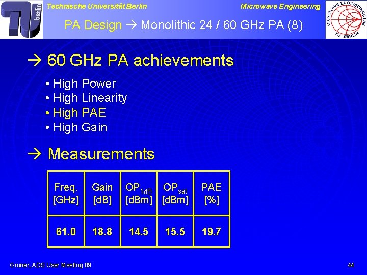
Technische Universität Berlin Microwave Engineering PA Design Monolithic 24 / 60 GHz PA (8) 60 GHz PA achievements • High Power • High Linearity • High PAE • High Gain Measurements Freq. [GHz] 61. 0 Gruner, ADS User Meeting 09 Gain OP 1 d. B OPsat [d. B] [d. Bm] PAE [%] 18. 8 19. 7 14. 5 15. 5 44
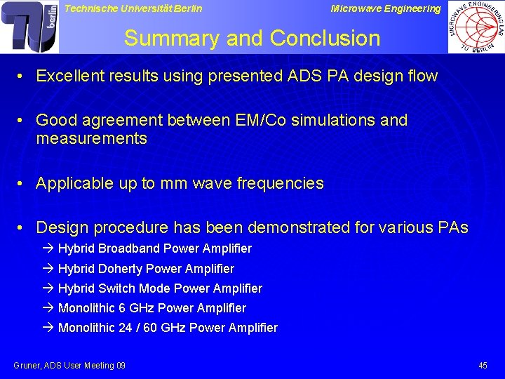
Technische Universität Berlin Microwave Engineering Summary and Conclusion • Excellent results using presented ADS PA design flow • Good agreement between EM/Co simulations and measurements • Applicable up to mm wave frequencies • Design procedure has been demonstrated for various PAs Hybrid Broadband Power Amplifier Hybrid Doherty Power Amplifier Hybrid Switch Mode Power Amplifier Monolithic 6 GHz Power Amplifier Monolithic 24 / 60 GHz Power Amplifier Gruner, ADS User Meeting 09 45

Technische Universität Berlin Microwave Engineering Summary and Conclusion Thanks Gruner, ADS User Meeting 09 46
- Slides: 46