Techniques for Test Power Reduction in Leading Edge
![Overview[1] Test power consumption is 3 x – 5 x the functional power Can Overview[1] Test power consumption is 3 x – 5 x the functional power Can](https://slidetodoc.com/presentation_image/42db62c24ac18d92f522e52a641a65d8/image-3.jpg)
![Compression Structure[2] 7 Compression Structure[2] 7](https://slidetodoc.com/presentation_image/42db62c24ac18d92f522e52a641a65d8/image-7.jpg)
![Channel Masking- Types [3] • Types Wide 0, Wide 1, Wide 2 • CUT Channel Masking- Types [3] • Types Wide 0, Wide 1, Wide 2 • CUT](https://slidetodoc.com/presentation_image/42db62c24ac18d92f522e52a641a65d8/image-13.jpg)
![Fill Techniques in Cadence ET[4] Toggle activity during scan test is high Reduce toggle Fill Techniques in Cadence ET[4] Toggle activity during scan test is high Reduce toggle](https://slidetodoc.com/presentation_image/42db62c24ac18d92f522e52a641a65d8/image-15.jpg)

![Synopsys Prime. Time-PX [5]- Fullscan mode Sequential Switching Power (in m. W) Repeat Pattern Synopsys Prime. Time-PX [5]- Fullscan mode Sequential Switching Power (in m. W) Repeat Pattern](https://slidetodoc.com/presentation_image/42db62c24ac18d92f522e52a641a65d8/image-21.jpg)
- Slides: 33

Techniques for Test Power Reduction in Leading Edge IP Using Cadence Encounter Test -ATPG: By Praveen Venkataramani 1

Objective To reduce dynamic power during test in scan based designs To obtain test vector sequences with minimum switching and pattern count without any loss in test coverage 2
![Overview1 Test power consumption is 3 x 5 x the functional power Can Overview[1] Test power consumption is 3 x – 5 x the functional power Can](https://slidetodoc.com/presentation_image/42db62c24ac18d92f522e52a641a65d8/image-3.jpg)
Overview[1] Test power consumption is 3 x – 5 x the functional power Can cause false failures due to IR drop as a result of high switching in scan test Shift Power Cause High toggle during shift Fix Reduction in overall toggle activity- Use fill techniques Capture Power Cause Toggle Activity due to circuit response Fix Using clock gating technique – Functional clock is gated from areas that are not required for functional operation at that time 3 3

Experimental Setup 45 nm Cortex A 8 ARM IP Functional clock - 600 MHz Flop Count – 130, 000 Clock Domains – 5 (only 1 Domain with 97%of flops is used for the experiments) Launch on Capture Length of Scan chains FULSCAN – 8 chains Average chain length : 17281 flip flops Longest chain length : 17344 flip flops Compression- 904 chains Average chain length: 152 flip flops Longest chain length: 155 flip flops Tool Used – Cadence Encounter Test (Cadence ET) Default setting Compaction Effort – Ultimate Fill – Random fill All Flops switch at capture 4

Vector Compression 5

Vector Compression Multiple chips are tested on an automated test equipment (ATE). Number of available scan channels(ports) from ATE is small compared to the ports in the CUT Available storage in ATE for test vectors Need for decompress and compress the test vectors used for test 6
![Compression Structure2 7 Compression Structure[2] 7](https://slidetodoc.com/presentation_image/42db62c24ac18d92f522e52a641a65d8/image-7.jpg)
Compression Structure[2] 7

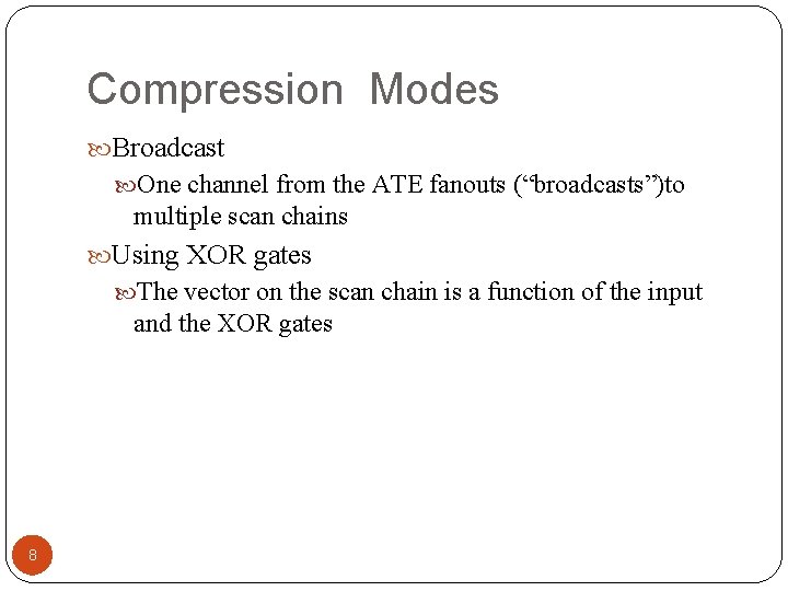
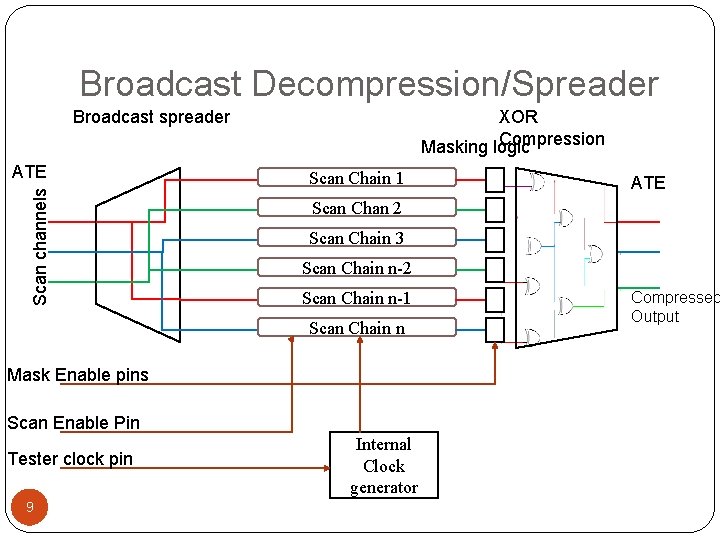
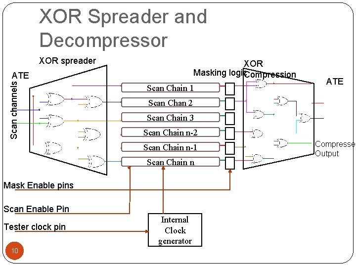
Compression Modes Broadcast One channel from the ATE fanouts (“broadcasts”)to multiple scan chains Using XOR gates The vector on the scan chain is a function of the input and the XOR gates 8

Broadcast Decompression/Spreader Broadcast spreader Scan channels ATE XOR Compression Masking logic Scan Chain 1 Scan Chan 2 Scan Chain 3 Scan Chain n-2 Scan Chain n-1 Scan Chain n Mask Enable pins Scan Enable Pin Tester clock pin 9 ATE Internal Clock generator Compressed Output

XOR Spreader and Decompressor XOR spreader Scan channels ATE XOR Masking logic. Compression Scan Chain 1 Scan Chan 2 Scan Chain 3 Scan Chain n-2 Scan Chain n-1 Scan Chain n Mask Enable pins Scan Enable Pin Tester clock pin 10 ATE Internal Clock generator Compressed Output

Channel Masking 11

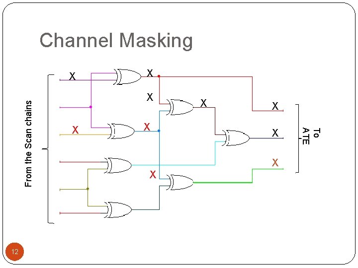
Channel Masking 12 X X X X X To ATE From the Scan chains X
![Channel Masking Types 3 Types Wide 0 Wide 1 Wide 2 CUT Channel Masking- Types [3] • Types Wide 0, Wide 1, Wide 2 • CUT](https://slidetodoc.com/presentation_image/42db62c24ac18d92f522e52a641a65d8/image-13.jpg)
Channel Masking- Types [3] • Types Wide 0, Wide 1, Wide 2 • CUT uses Wide 2 Mask logic • Contains 2 Mask registers R 0 and R 1 • Mask register is pre-loaded before scan out. • Sets the ‘X’ to value in the Mask bit • Prevents output 13 data from corruption

Scan Shift Toggle Reduction 14
![Fill Techniques in Cadence ET4 Toggle activity during scan test is high Reduce toggle Fill Techniques in Cadence ET[4] Toggle activity during scan test is high Reduce toggle](https://slidetodoc.com/presentation_image/42db62c24ac18d92f522e52a641a65d8/image-15.jpg)
Fill Techniques in Cadence ET[4] Toggle activity during scan test is high Reduce toggle activity using fill techniques Random Repeat ‘ 0’ or ‘ 1’ Method 1: explicitly specify the fill technique Method 2: specify the allowed percentage toggle activity Method 3: Dual fill, combination of repeat and random fill. 15

Filling of “Don’t-care” Bits- Fullscan Mode (Cadence ET®) 16

Filling of “Don’t-care” Bits- Fullscan Mode (Cadence ET®) 17

Average Toggle Activity during scan shift in Fullscan Mode 18

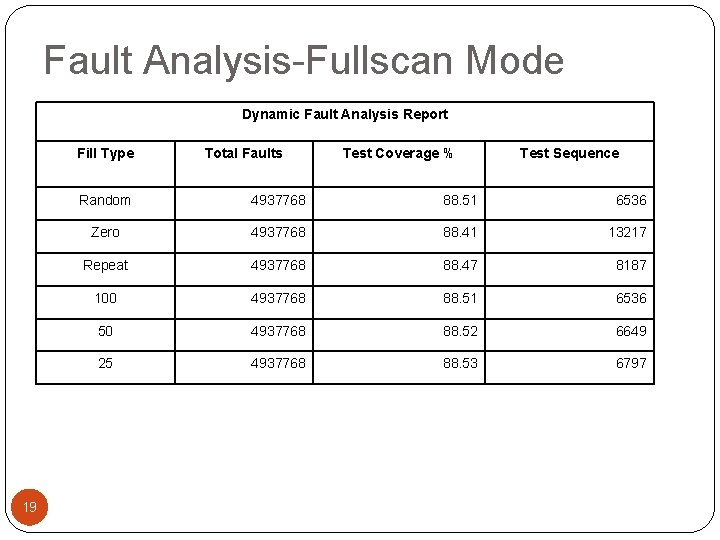
Fault Analysis-Fullscan Mode Dynamic Fault Analysis Report Fill Type 19 Total Faults Test Coverage % Test Sequence Random 4937768 88. 51 6536 Zero 4937768 88. 41 13217 Repeat 4937768 88. 47 8187 100 4937768 88. 51 6536 50 4937768 88. 52 6649 25 4937768 88. 53 6797

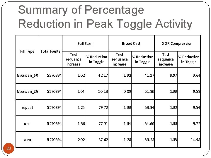
Summary of Percentage Reduction in Peak Toggle Activity Full Scan Fill Type 20 Total Faults Test sequence increase Broad Cast % Reduction in Toggle Test sequence increase XOR Compression % Reduction in Toggle Test sequence increase % Reduction in Toggle Maxscan_50 5270394 1. 02 42. 17 1. 02 41. 17 0. 97 0. 64 Maxscan_25 5270394 1. 04 50. 13 0. 89 51. 30 1. 00 9. 53 repeat 5270394 1. 25 79. 72 1. 00 53. 94 1. 02 9. 54 one 5270394 1. 36 77. 01 1. 04 54. 60 1. 03 9. 72 zero 5270394 2. 02 87. 62 1. 28 53. 23 1. 35 14. 98
![Synopsys Prime TimePX 5 Fullscan mode Sequential Switching Power in m W Repeat Pattern Synopsys Prime. Time-PX [5]- Fullscan mode Sequential Switching Power (in m. W) Repeat Pattern](https://slidetodoc.com/presentation_image/42db62c24ac18d92f522e52a641a65d8/image-21.jpg)
Synopsys Prime. Time-PX [5]- Fullscan mode Sequential Switching Power (in m. W) Repeat Pattern Random 21 Initial % Reduction Final % Reduction 3 0. 0281 0. 0166 40. 9 0. 0167 40. 5 4 0. 0293 0. 0176 39. 9 0. 0174 39. 9 5 0. 0286 0. 0176 38. 4 0. 0174 39. 5

IR Drop Analysis 22

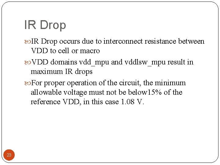
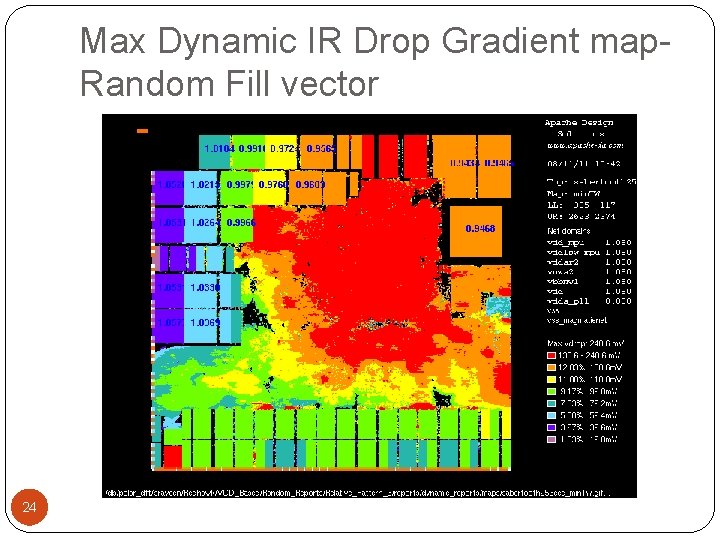
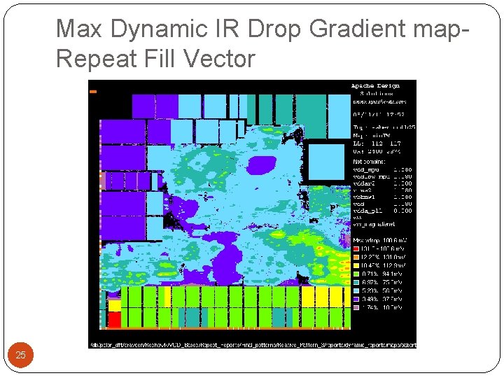
IR Drop occurs due to interconnect resistance between VDD to cell or macro VDD domains vdd_mpu and vddlsw_mpu result in maximum IR drops For properation of the circuit, the minimum allowable voltage must not be below 15% of the reference VDD, in this case 1. 08 V. 23

Max Dynamic IR Drop Gradient map. Random Fill vector 24

Max Dynamic IR Drop Gradient map. Repeat Fill Vector 25

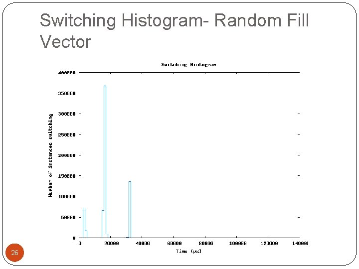
Switching Histogram- Random Fill Vector 26

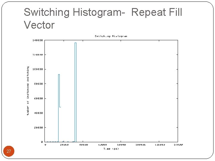
Switching Histogram- Repeat Fill Vector 27

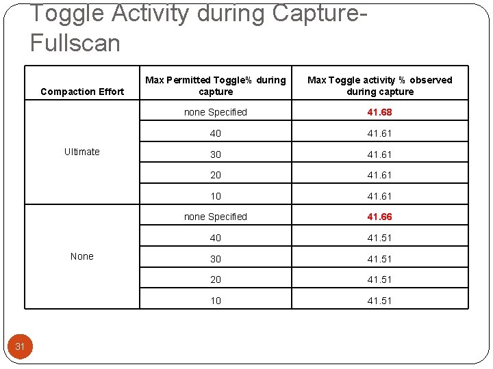
Scan Capture Toggle Reduction Reason for toggle during scan capture What is clock gating? Results from Cadence ET 28

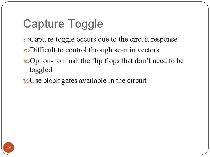
Capture Toggle Capture toggle occurs due to the circuit response Difficult to control through scan in vectors Option- to mask the flip flops that don’t need to be toggled Use clock gates available in the circuit 29

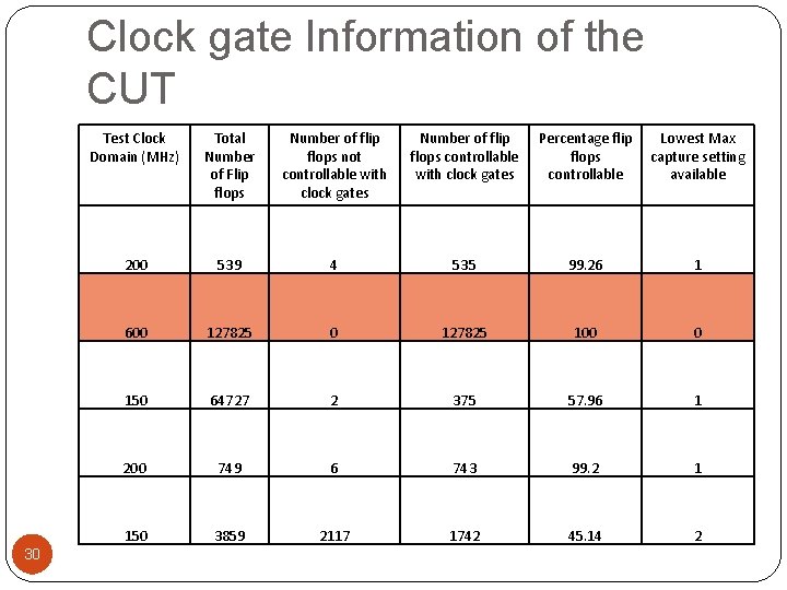
Clock gate Information of the CUT 30 Test Clock Domain (MHz) Total Number of Flip flops Number of flip flops not controllable with clock gates Number of flip flops controllable with clock gates Percentage flip flops controllable Lowest Max capture setting available 200 539 4 535 99. 26 1 600 127825 100 0 150 64727 2 375 57. 96 1 200 749 6 743 99. 2 1 150 3859 2117 1742 45. 14 2

Toggle Activity during Capture. Fullscan Compaction Effort Ultimate None 31 Max Permitted Toggle% during capture Max Toggle activity % observed during capture none Specified 41. 68 40 41. 61 30 41. 61 20 41. 61 10 41. 61 none Specified 41. 66 40 41. 51 30 41. 51 20 41. 51 10 41. 51

Future work Pattern Generation and analysis for reduction in toggle activity during scan capture. Use the generated vector on ATE to test the CUT 32

1. 33 References Ravi, S. , "Power-aware test: Challenges and solutions, " Test Conference, 2007. ITC 2007. IEEE International , vol. , no. , pp. 1 -10, 21 -26 Oct. 2007 doi: 10. 1109/TEST. 2007. 4437660 2. http: //www. cadence. com/rl/Resources/conference_papers/3. 7 Presentation. pdf 3. Vivek Chickermane, Brian Foutz, and Brion Keller. 2004. Channel Masking Synthesis for Efficient On-Chip Test Compression. In Proceedings of the International Test Conference on International Test Conference (ITC '04). IEEE Computer Society, Washington, DC, USA, 452 -461. 4. Encounter Test Low Power user guide 5. Synopsys Prime. Time PX user guide 6. Apache Redhawk user guide 7. “The Power of RTL Clock-gating”, by Mitch Dale, http: //chipdesignmag. com/display. php? article. Id=915