Teaching Digital Logic courses with Altera Technology Tutorial
![Simple Project SW[0] KEY[1] LED[9] 12 Input Reset_N Clock … 10 -bit Shift Register Simple Project SW[0] KEY[1] LED[9] 12 Input Reset_N Clock … 10 -bit Shift Register](https://slidetodoc.com/presentation_image_h2/89d54e8a65552fdb5b4df86b7e20a290/image-12.jpg)
![Step 8: See your design work on the board Press the KEY[0] to clock Step 8: See your design work on the board Press the KEY[0] to clock](https://slidetodoc.com/presentation_image_h2/89d54e8a65552fdb5b4df86b7e20a290/image-18.jpg)
![Circuit Diagram KEY[0] FSM Fast Clock Divider Slow enable Clock 10 -bit Shift Register Circuit Diagram KEY[0] FSM Fast Clock Divider Slow enable Clock 10 -bit Shift Register](https://slidetodoc.com/presentation_image_h2/89d54e8a65552fdb5b4df86b7e20a290/image-22.jpg)

![Signal. Tap II Operation USB-Blaster cable KEY[0] KEY[1] Signal. Tap Module FSM enable Clock Signal. Tap II Operation USB-Blaster cable KEY[0] KEY[1] Signal. Tap Module FSM enable Clock](https://slidetodoc.com/presentation_image_h2/89d54e8a65552fdb5b4df86b7e20a290/image-31.jpg)
![Lab 4: Counters Suggested solution Part 1 assign Enable_0 = SW[1]; Toggle. FF (Enable_0, Lab 4: Counters Suggested solution Part 1 assign Enable_0 = SW[1]; Toggle. FF (Enable_0,](https://slidetodoc.com/presentation_image_h2/89d54e8a65552fdb5b4df86b7e20a290/image-47.jpg)
- Slides: 49

Teaching Digital Logic courses with Altera Technology Tutorial #1

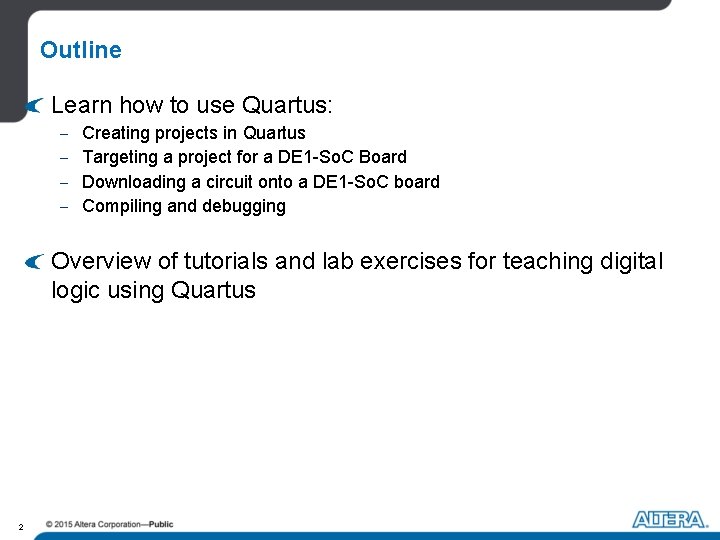
Outline Learn how to use Quartus: - Creating projects in Quartus Targeting a project for a DE 1 -So. C Board Downloading a circuit onto a DE 1 -So. C board Compiling and debugging Overview of tutorials and lab exercises for teaching digital logic using Quartus 2

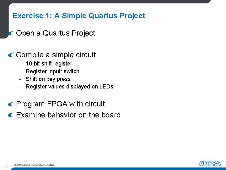
Exercise 1: A Simple Quartus Project Open a Quartus Project Compile a simple circuit - 10 -bit shift register Register input: switch Shift on key press Register values displayed on LEDs Program FPGA with circuit Examine behavior on the board 3

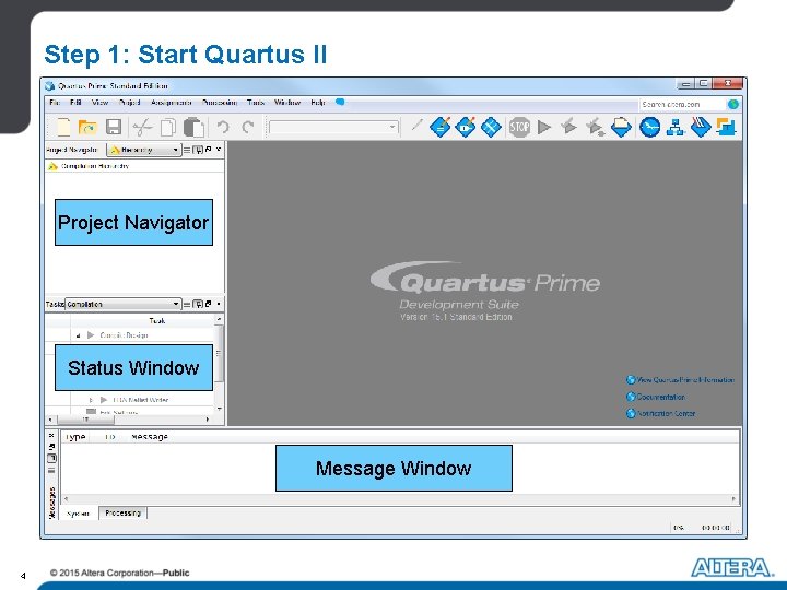
Step 1: Start Quartus II Project Navigator Status Window Message Window 4

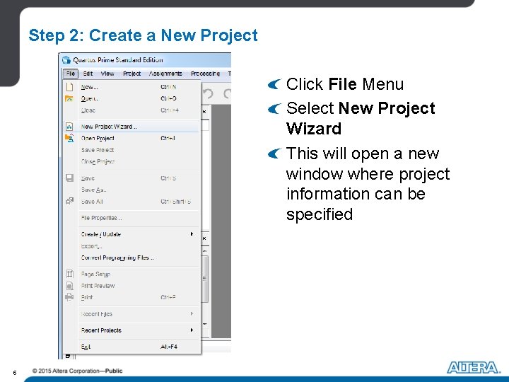
Step 2: Create a New Project Click File Menu Select New Project Wizard This will open a new window where project information can be specified 5

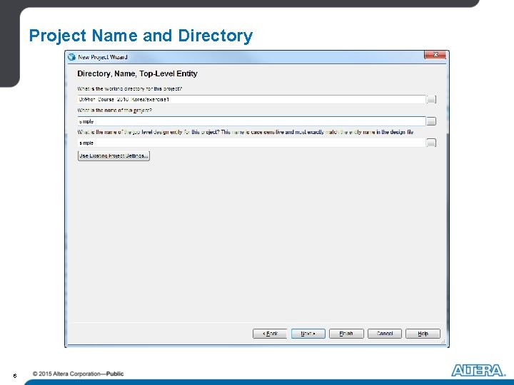
Project Name and Directory 6

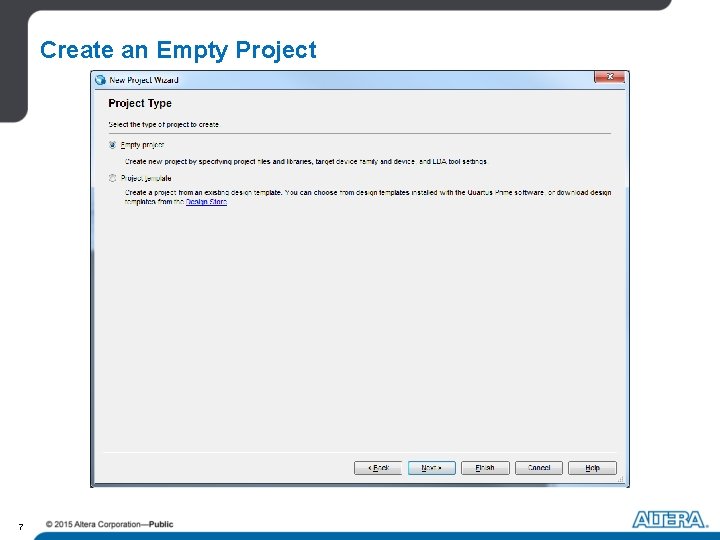
Create an Empty Project 7

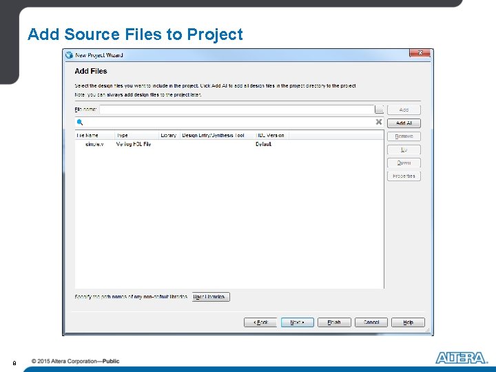
Add Source Files to Project 8

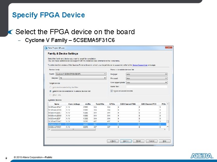
Specify FPGA Device Select the FPGA device on the board - Cyclone V Family – 5 CSEMA 5 F 31 C 6 9

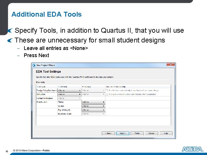
Additional EDA Tools Specify Tools, in addition to Quartus II, that you will use These are unnecessary for small student designs - Leave all entries as <None> - Press Next 10

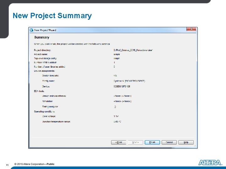
New Project Summary 11
![Simple Project SW0 KEY1 LED9 12 Input ResetN Clock 10 bit Shift Register Simple Project SW[0] KEY[1] LED[9] 12 Input Reset_N Clock … 10 -bit Shift Register](https://slidetodoc.com/presentation_image_h2/89d54e8a65552fdb5b4df86b7e20a290/image-12.jpg)
Simple Project SW[0] KEY[1] LED[9] 12 Input Reset_N Clock … 10 -bit Shift Register LED[2] LED[1] LED[0]

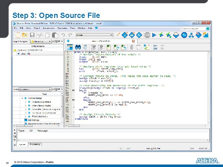
Step 3: Open Source File 13

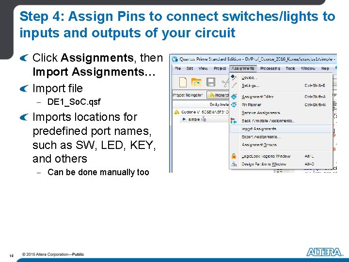
Step 4: Assign Pins to connect switches/lights to inputs and outputs of your circuit Click Assignments, then Import Assignments… Import file - DE 1_So. C. qsf Imports locations for predefined port names, such as SW, LED, KEY, and others - Can be done manually too 14

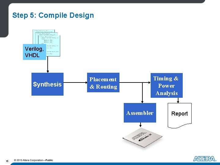
Step 5: Compile Design Verilog, VHDL Synthesis Placement & Routing Timing & Power Analysis Assembler 15 Report

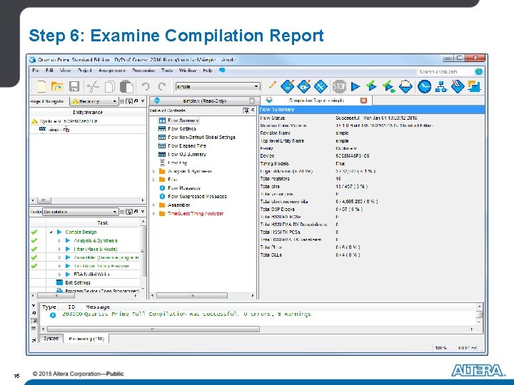
Step 6: Examine Compilation Report 16

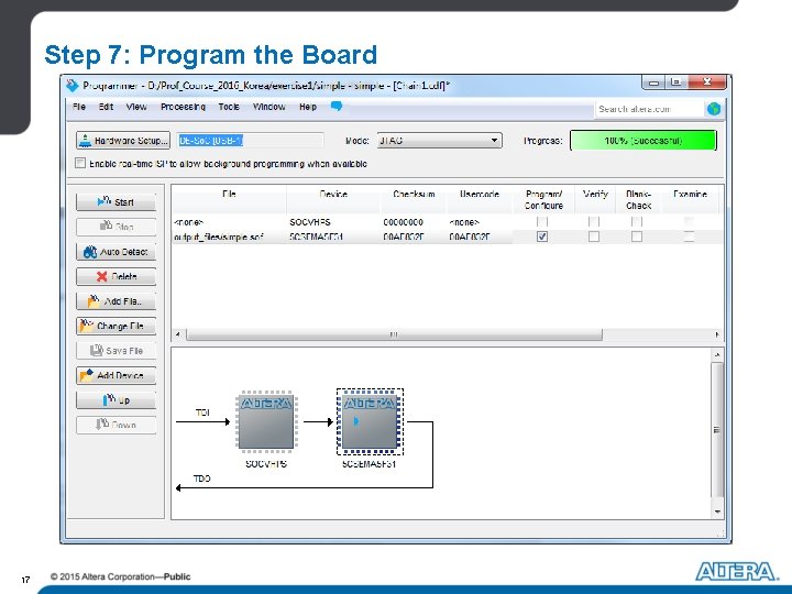
Step 7: Program the Board 17
![Step 8 See your design work on the board Press the KEY0 to clock Step 8: See your design work on the board Press the KEY[0] to clock](https://slidetodoc.com/presentation_image_h2/89d54e8a65552fdb5b4df86b7e20a290/image-18.jpg)
Step 8: See your design work on the board Press the KEY[0] to clock the circuit SW[0] is the input to the shift register Reset the shift register using KEY[1] SW[0] KEY[1] KEY[0] Input Reset_N Clock 10 -bit Shift Register Red LEDs 18

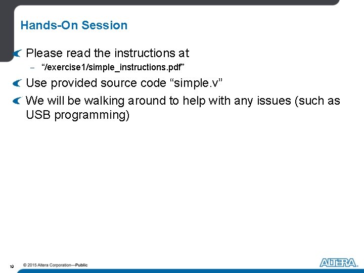
Hands-On Session Please read the instructions at - “/exercise 1/simple_instructions. pdf” Use provided source code “simple. v” We will be walking around to help with any issues (such as USB programming) 19

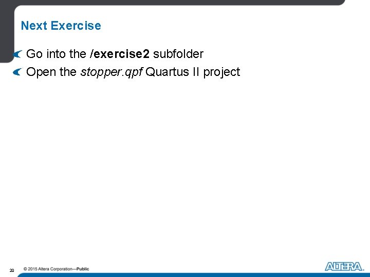
Next Exercise Go into the /exercise 2 subfolder Open the stopper. qpf Quartus II project 20

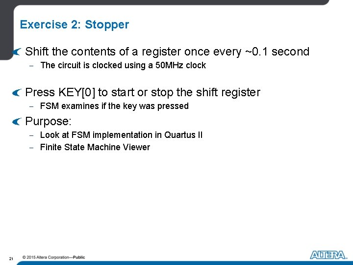
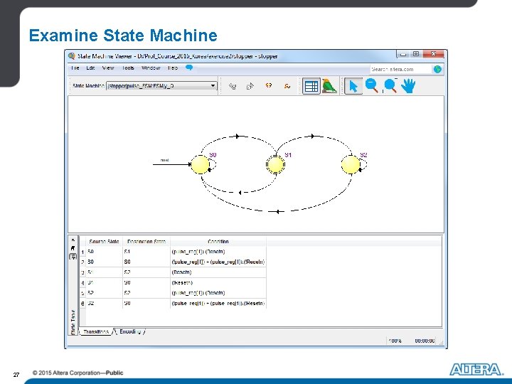
Exercise 2: Stopper Shift the contents of a register once every ~0. 1 second - The circuit is clocked using a 50 MHz clock Press KEY[0] to start or stop the shift register - FSM examines if the key was pressed Purpose: - Look at FSM implementation in Quartus II - Finite State Machine Viewer 21
![Circuit Diagram KEY0 FSM Fast Clock Divider Slow enable Clock 10 bit Shift Register Circuit Diagram KEY[0] FSM Fast Clock Divider Slow enable Clock 10 -bit Shift Register](https://slidetodoc.com/presentation_image_h2/89d54e8a65552fdb5b4df86b7e20a290/image-22.jpg)
Circuit Diagram KEY[0] FSM Fast Clock Divider Slow enable Clock 10 -bit Shift Register Red LEDs 22

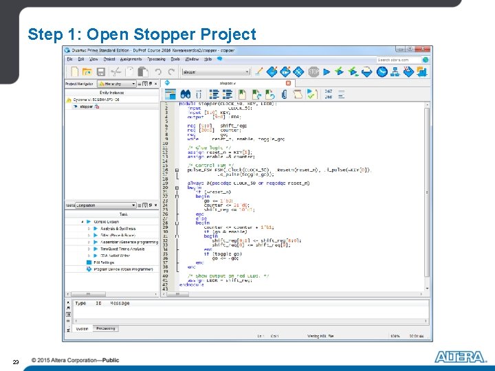
Step 1: Open Stopper Project 23

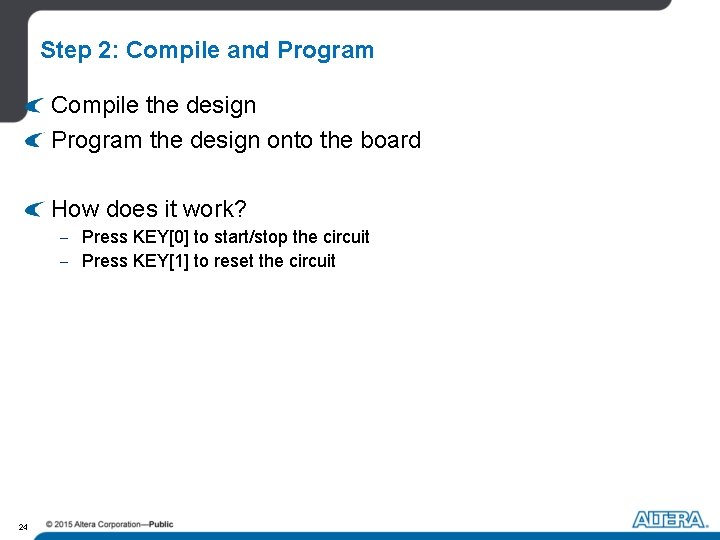
Step 2: Compile and Program Compile the design Program the design onto the board How does it work? - Press KEY[0] to start/stop the circuit - Press KEY[1] to reset the circuit 24

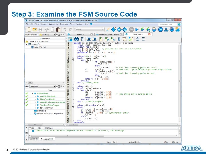
Step 3: Examine the FSM Source Code 25

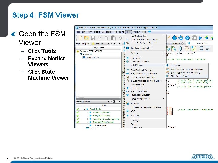
Step 4: FSM Viewer Open the FSM Viewer - Click Tools - Expand Netlist Viewers - Click State Machine Viewer 26

Examine State Machine 27

Hands-On Session Please read the instructions at - “/exercise 2/stopper_instructions. pdf” Use provided project “stopper. qpf” 28

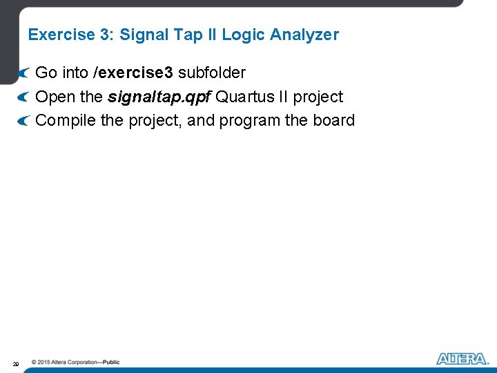
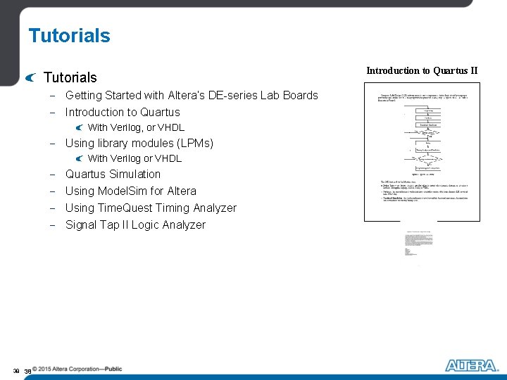
Exercise 3: Signal Tap II Logic Analyzer Go into /exercise 3 subfolder Open the signaltap. qpf Quartus II project Compile the project, and program the board 29

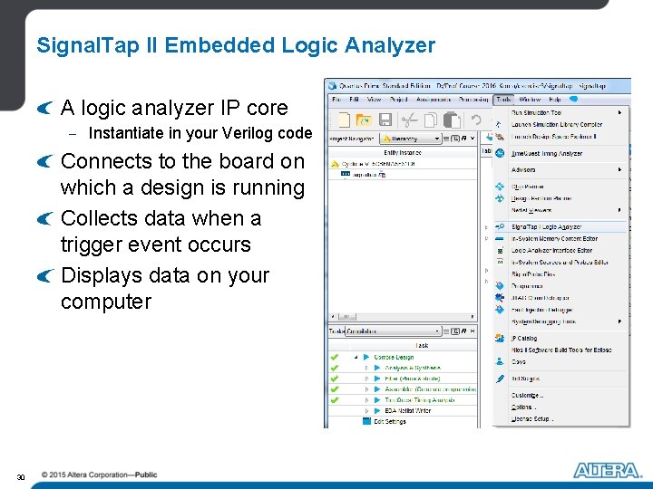
Signal. Tap II Embedded Logic Analyzer A logic analyzer IP core - Instantiate in your Verilog code Connects to the board on which a design is running Collects data when a trigger event occurs Displays data on your computer 30
![Signal Tap II Operation USBBlaster cable KEY0 KEY1 Signal Tap Module FSM enable Clock Signal. Tap II Operation USB-Blaster cable KEY[0] KEY[1] Signal. Tap Module FSM enable Clock](https://slidetodoc.com/presentation_image_h2/89d54e8a65552fdb5b4df86b7e20a290/image-31.jpg)
Signal. Tap II Operation USB-Blaster cable KEY[0] KEY[1] Signal. Tap Module FSM enable Clock 10 -bit Shift Register Clock FPGA Red LEDs 31

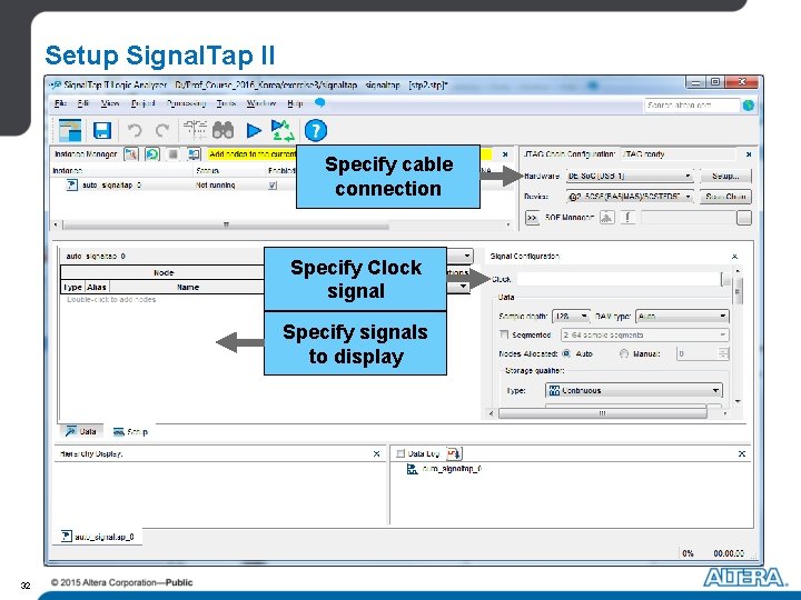
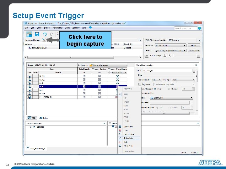
Setup Signal. Tap II Specify cable connection Specify Clock signal Specify signals to display 32

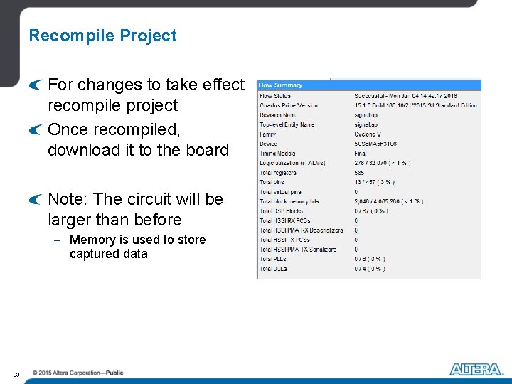
Recompile Project For changes to take effect recompile project Once recompiled, download it to the board Note: The circuit will be larger than before - Memory is used to store captured data 33

Setup Event Trigger Click here to begin capture 34

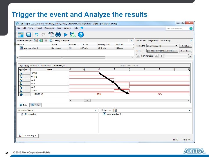
Trigger the event and Analyze the results 35

Hands-On Session Please read the instructions at - “/exercise 3/signtaltap_instructions. pdf” Use provided project “signaltap. qpf” 36

Summary of Tutorial #1 Learned how to - 37 Use Quartus II CAD Software Compile projects in Quartus II Target design onto DE 1 -So. C View results of compilation Use Signal. Tap II

Tutorials - Getting Started with Altera’s DE-series Lab Boards - Introduction to Quartus With Verilog, or VHDL - Using library modules (LPMs) With Verilog or VHDL - Quartus Simulation - Using Model. Sim for Altera - Using Time. Quest Timing Analyzer - Signal Tap II Logic Analyzer 38 38 Introduction to Quartus II

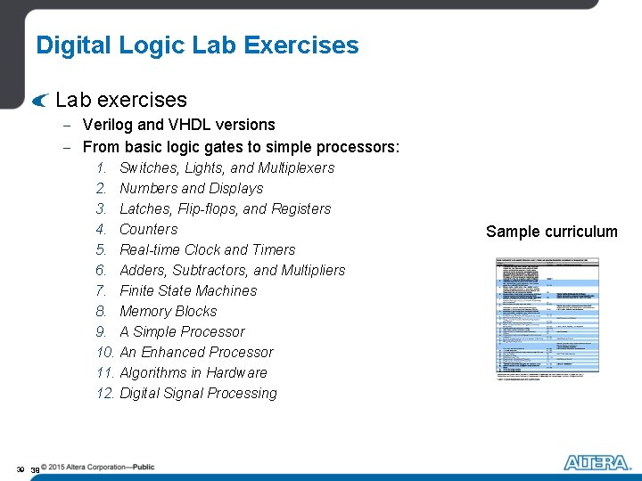
Digital Logic Lab Exercises Lab exercises - Verilog and VHDL versions - From basic logic gates to simple processors: 1. Switches, Lights, and Multiplexers 2. Numbers and Displays 3. Latches, Flip-flops, and Registers 4. Counters 5. Real-time Clock and Timers 6. Adders, Subtractors, and Multipliers 7. Finite State Machines 8. Memory Blocks 9. A Simple Processor 10. An Enhanced Processor 11. Algorithms in Hardware 12. Digital Signal Processing 39 39 Sample curriculum

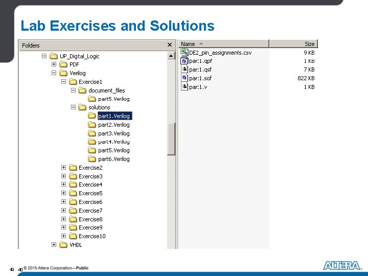
Lab Exercises and Solutions Exercises and complete solutions on U. P. web site - Password protected (Professors/Lecturers) - Includes all Quartus II projects - Includes all figures and source text (allows Instructors to add their own material) 40 40

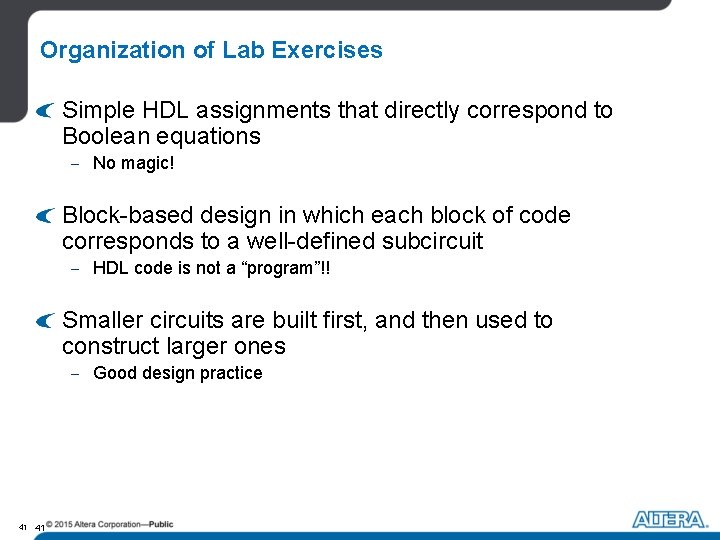
Organization of Lab Exercises Simple HDL assignments that directly correspond to Boolean equations - No magic! Block-based design in which each block of code corresponds to a well-defined subcircuit - HDL code is not a “program”!! Smaller circuits are built first, and then used to construct larger ones - Good design practice 41 41

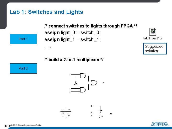
Lab 1: Switches and Lights /* connect switches to lights through FPGA */ Part 1 assign light_0 = switch_0; assign light_1 = switch_1; . . . /* build a 2 -to-1 multiplexer */ Part 2 42 42 Suggested solution

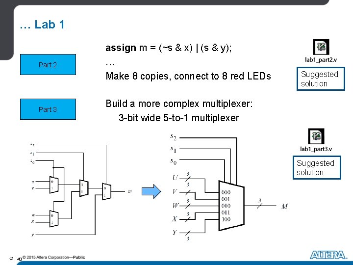
… Lab 1 Part 2 Part 3 assign m = (~s & x) | (s & y); … Make 8 copies, connect to 8 red LEDs Suggested solution Build a more complex multiplexer: 3 -bit wide 5 -to-1 multiplexer Suggested solution 43 43

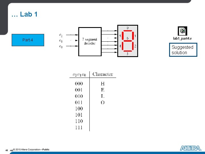
… Lab 1 Part 4 Suggested solution 44 44

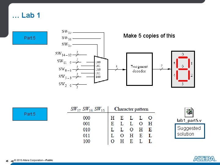
… Lab 1 Part 5 Make 5 copies of this Part 5 Suggested solution 45 45

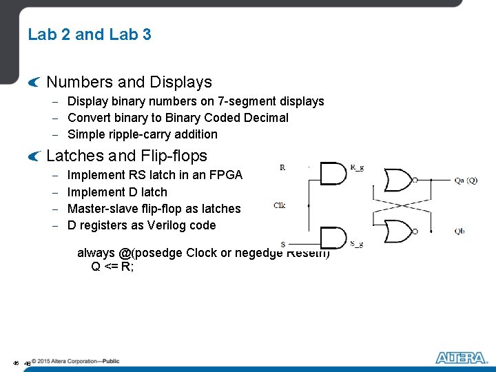
Lab 2 and Lab 3 Numbers and Displays - Display binary numbers on 7 -segment displays - Convert binary to Binary Coded Decimal - Simple ripple-carry addition Latches and Flip-flops - Implement RS latch in an FPGA Implement D latch Master-slave flip-flop as latches D registers as Verilog code always @(posedge Clock or negedge Resetn) Q <= R; 46 46
![Lab 4 Counters Suggested solution Part 1 assign Enable0 SW1 Toggle FF Enable0 Lab 4: Counters Suggested solution Part 1 assign Enable_0 = SW[1]; Toggle. FF (Enable_0,](https://slidetodoc.com/presentation_image_h2/89d54e8a65552fdb5b4df86b7e20a290/image-47.jpg)
Lab 4: Counters Suggested solution Part 1 assign Enable_0 = SW[1]; Toggle. FF (Enable_0, Clock, Clear, Count_0); assign Enable_1 = Count_0 & Enable_0; Toggle. FF (Enable_1, Clock, Clear, Count_1); . . .

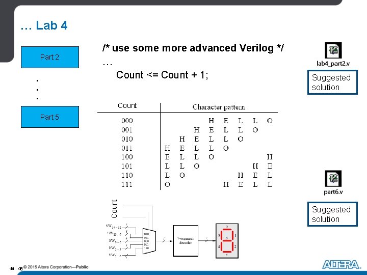
… Lab 4 Part 2 . . . /* use some more advanced Verilog */ … Count <= Count + 1; Suggested solution Count Part 5 48 48 Suggested solution

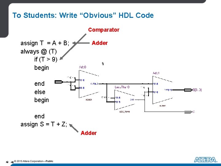
To Students: Write “Obvious” HDL Code Comparator Adder assign T = A + B; always @ (T) if (T > 9) begin Z = 6; C = 1; end else Multiplexer that selects begin constants Z = 0; C = 0; end assign S = T + Z; Adder 49 49