TCT measurements with CHESS1 chip I Mandi Joef
- Slides: 11

TCT measurements with CHESS-1 chip I. Mandić, Jožef Stefan Institute 1

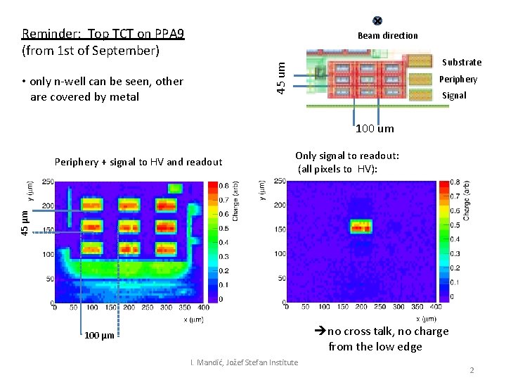
Reminder: Top TCT on PPA 9 (from 1 st of September) Beam direction 45 um Substrate • only n-well can be seen, other are covered by metal Periphery Signal 100 um Only signal to readout: (all pixels to HV): 45 μm Periphery + signal to HV and readout no cross talk, no charge from the low edge 100 μm I. Mandić, Jožef Stefan Institute 2

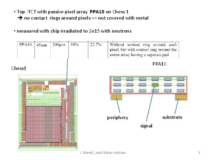
• Top -TCT with passive pixel array PPA 10 on Chess 1 no contact rings around pixels => not covered with metal • measured with chip irradiated to 2 e 15 with neutrons PPA 10 Chess 1 substrate periphery signal I. Mandić, Jožef Stefan Institute 3

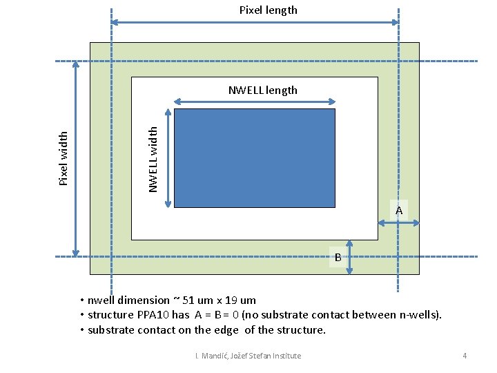
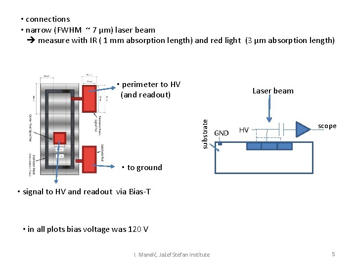
Pixel length NWELL width Pixel width NWELL length A B • nwell dimension ~ 51 um x 19 um • structure PPA 10 has A = B = 0 (no substrate contact between n-wells). • substrate contact on the edge of the structure. I. Mandić, Jožef Stefan Institute 4

• connections • narrow (FWHM ~ 7 μm) laser beam measure with IR ( 1 mm absorption length) and red light (3 μm absorption length) • perimeter to HV (and readout) substrate Laser beam GND HV scope • to ground • signal to HV and readout via Bias-T • in all plots bias voltage was 120 V I. Mandić, Jožef Stefan Institute 5

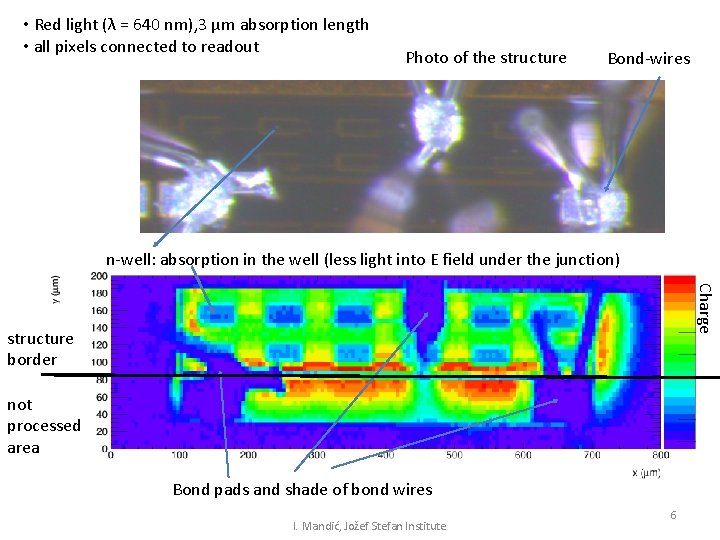
• Red light (λ = 640 nm), 3 μm absorption length • all pixels connected to readout Photo of the structure Bond-wires n-well: absorption in the well (less light into E field under the junction) Charge structure border not processed area Bond pads and shade of bond wires I. Mandić, Jožef Stefan Institute 6

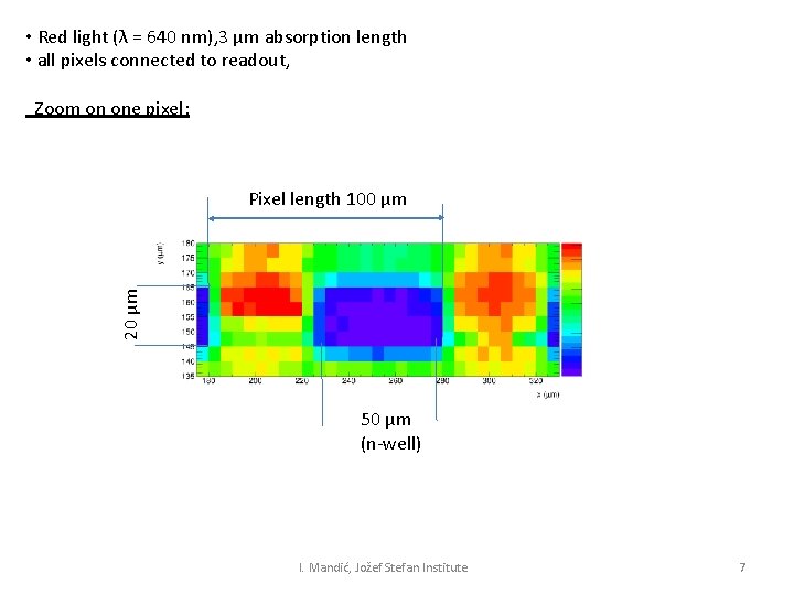
• Red light (λ = 640 nm), 3 μm absorption length • all pixels connected to readout, Zoom on one pixel: 20 μm Pixel length 100 μm 50 μm (n-well) I. Mandić, Jožef Stefan Institute 7

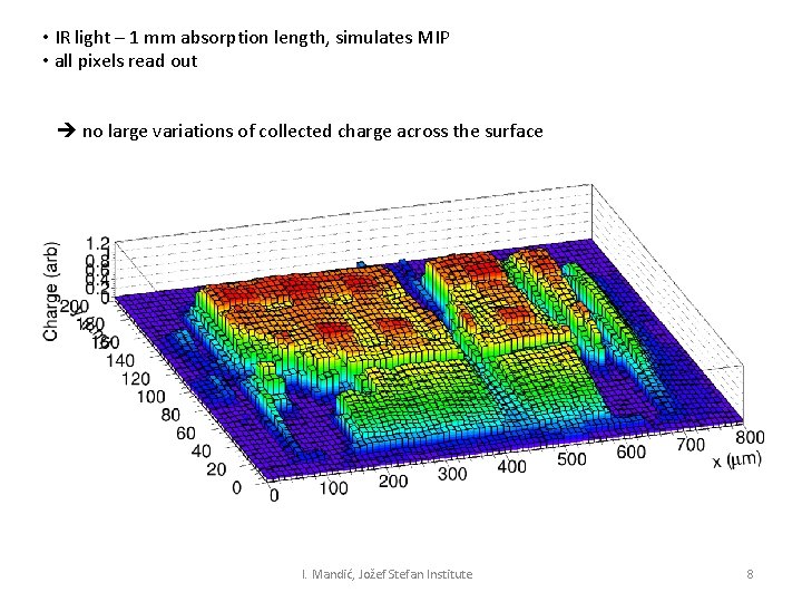
• IR light – 1 mm absorption length, simulates MIP • all pixels read out no large variations of collected charge across the surface I. Mandić, Jožef Stefan Institute 8

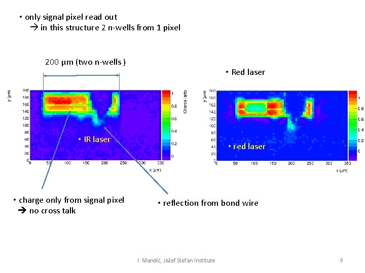
• only signal pixel read out in this structure 2 n-wells from 1 pixel 200 μm (two n-wells ) • Red laser • IR laser • charge only from signal pixel no cross talk • red laser • reflection from bond wire I. Mandić, Jožef Stefan Institute 9

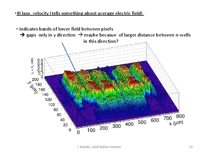
• IR lase, velocity (tells something about average electric field) • indicates bands of lower field between pixels gaps only in y direction maybe becasue of larger distance between n-wells in this direction? I. Mandić, Jožef Stefan Institute 10

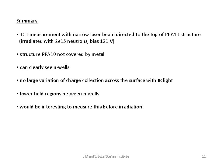
Summary • TCT measurement with narrow laser beam directed to the top of PPA 10 structure (irradiated with 2 e 15 neutrons, bias 120 V) • structure PPA 10 not covered by metal • can clearly see n-wells • no large variation of charge collection across the surface with IR light • lower field regions between n-wells • would be interesting to measure this before irradiation I. Mandić, Jožef Stefan Institute 11