
TCT for the characterization of silicon interfaces obtained
TCT for the characterization of silicon interfaces obtained by CMOS compatible wafer bonding Jacopo Bronuzzi, jacopo. bronuzzi@cern. ch Alessandro Mapelli 1, Michael Moll 1, Luciano Musa 1, Walter Snoeys 1, Petra Riedler 1, Eric Rouchouze 3, Catherine Charrier 3, Frank Fournel 3, Jean-Michel Sallese 2 1 Detector Technologies Group, EP Department, CERN, 2 Group of Electron Device Modeling an Technology, EDLAB, EPFL, 3 Silicon Platform, CEA-LETI 1 https: //ep-dt. web. cern. ch/ 2 http: //www. leti-cea. fr/cea-tech/leti/Pages/innovation-industrielle/innover-avec-le-Leti/LETI-3 S. aspx 3 https: //edlab. epfl. ch/ RD 50 – Workshop 20 November 2017
Outline • CMOS compatible wafer bonding • Bonded Monolithic Active Silicon Sensors • TCT for bonding interface characterization • Analytical modeling of TCT for bonding interface characterization • Fabrication of test structure for TCT bonding interface characterization • Electrical injection TCT • • Working principle Clean room fabrication of test structures Measurements setup description Measurements and proof of principle J. Bronuzzi - RD 50 Workshop 20 November 2017 2
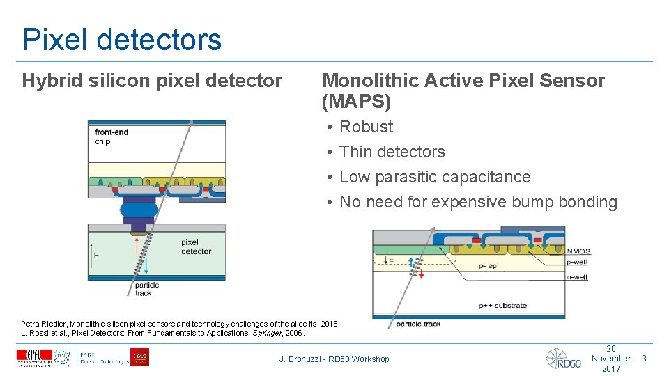
Pixel detectors Hybrid silicon pixel detector Monolithic Active Pixel Sensor (MAPS) • • Robust Thin detectors Low parasitic capacitance No need for expensive bump bonding Petra Riedler, Monolithic silicon pixel sensors and technology challenges of the alice its, 2015. L. Rossi et al. , Pixel Detectors: From Fundamentals to Applications, Springer, 2006. J. Bronuzzi - RD 50 Workshop 20 November 2017 3
Fabrication of monolithic pixel detectors Sensor driven Electronics driven • Low resistivity silicon • High performance electronics • Low performance sensing (small depletion region) • High resistivity silicon • Difficult electronics design • High performance sensing (large depletion region) L. Rossi et al. , Pixel Detectors: From Fundamentals to Applications, Springer, 2006. J. Bronuzzi - RD 50 Workshop 20 November 2017 4
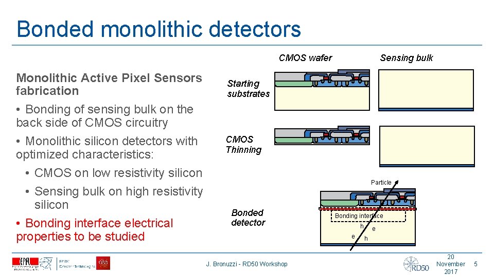
Bonded monolithic detectors CMOS wafer Monolithic Active Pixel Sensors fabrication • Bonding of sensing bulk on the back side of CMOS circuitry • Monolithic silicon detectors with optimized characteristics: • CMOS on low resistivity silicon • Sensing bulk on high resistivity silicon • Bonding interface electrical properties to be studied Sensing bulk Starting substrates CMOS Thinning Particle Bonded detector Bonding interface h e J. Bronuzzi - RD 50 Workshop e h 20 November 2017 5
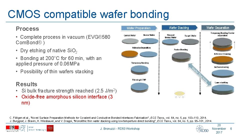
CMOS compatible wafer bonding Process • Complete process in vacuum (EVG® 580 Com. Bond® ) • Dry etching of native Si. O 2 • Bonding at 200°C for 60 min, with an applied pressure of 0. 06 MPa • Possibility of thin wafers stacking Results • Si bulk fracture strength reached (2. 5 J/m 2) • Oxide-free amorphous silicon interface (3 nm) C. Flötgen et al. , “Novel Surface Preparation Methods for Covalent and Conductive Bonded Interfaces Fabrication”, ECS Trans. , vol. 64, no. 5, pp. 103– 110, 2014. J. Burggraf, J. Bravin, H. Wiesbauer, and V. Dragoi, “Monolithic thin wafer stacking using low temperture direct bonding”, ECS Trans. , vol. 64, no. 5, pp. 95– 101, 2014. J. Bronuzzi - RD 50 Workshop 20 November 2017 6
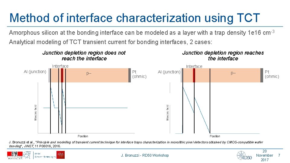
Method of interface characterization using TCT Amorphous silicon at the bonding interface can be modeled as a layer with a trap density 1 e 16 cm-3 Analytical modeling of TCT transient current for bonding interfaces, 2 cases: Junction depletion region does not reach the interface Junction depletion region reaches the interface Interface Al (junction) Interface p-- Pt (ohmic) Al (junction) Pt (ohmic) p-- J. Bronuzzi et al. , “Principle and modelling of transient current technique for interface traps characterization in monolithic pixel detectors obtained by CMOS-compatible wafer bonding”, JINST, 11 P 08016, 2016. J. Bronuzzi - RD 50 Workshop 20 November 2017 7

TCT for bonding interface traps Different applied voltage TCT current 0. 5 V Electric field 3 -5 -7 V interface not included in depletion region interface included in depletion region TCT current not affected by interface TCT current affected by interface J. Bronuzzi - RD 50 Workshop 20 November 2017 8

TCT for bonding interface traps Different traps type Acceptors Donors generate positive charge negative charge TCT current Acceptors and Donors Electric field Charge compensation Electric field decreased Electric field increases No discontinuity in electric field Not clear signature in TCT signal TCT current affected by interface Not clear signature in TCT signal J. Bronuzzi - RD 50 Workshop 20 November 2017 9
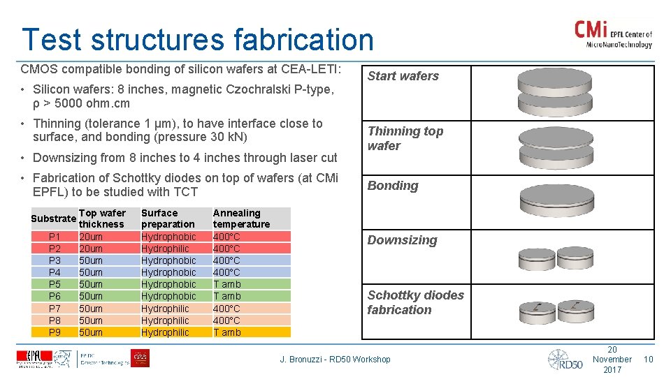
Test structures fabrication CMOS compatible bonding of silicon wafers at CEA-LETI: • Silicon wafers: 8 inches, magnetic Czochralski P-type, ρ > 5000 ohm. cm • Thinning (tolerance 1 µm), to have interface close to surface, and bonding (pressure 30 k. N) • Downsizing from 8 inches to 4 inches through laser cut • Fabrication of Schottky diodes on top of wafers (at CMi EPFL) to be studied with TCT Substrate P 1 P 2 P 3 P 4 P 5 P 6 P 7 P 8 P 9 Top wafer thickness 20 um 50 um 50 um Surface preparation Hydrophobic Hydrophilic Hydrophobic Hydrophilic Annealing temperature 400°C T amb 400°C T amb Start wafers Thinning top wafer Bonding Downsizing Schottky diodes fabrication J. Bronuzzi - RD 50 Workshop 20 November 2017 10
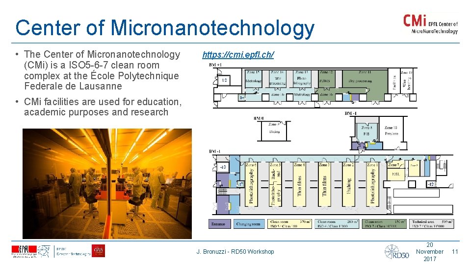
Center of Micronanotechnology • The Center of Micronanotechnology (CMi) is a ISO 5 -6 -7 clean room complex at the École Polytechnique Federale de Lausanne https: //cmi. epfl. ch/ • CMi facilities are used for education, academic purposes and research J. Bronuzzi - RD 50 Workshop 20 November 2017 11
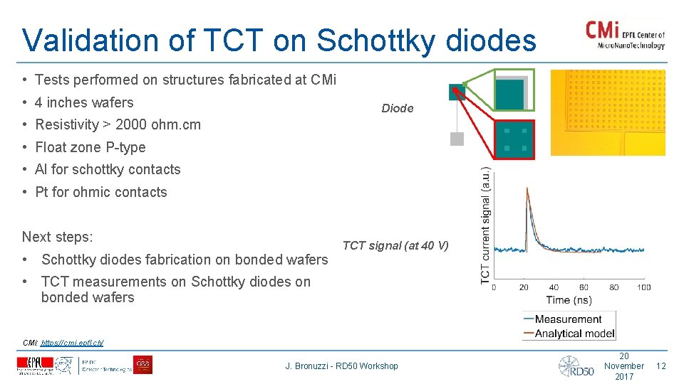
Validation of TCT on Schottky diodes • Tests performed on structures fabricated at CMi • 4 inches wafers Diode • Resistivity > 2000 ohm. cm • Float zone P-type • Al for schottky contacts • Pt for ohmic contacts Next steps: • Schottky diodes fabrication on bonded wafers TCT signal (at 40 V) • TCT measurements on Schottky diodes on bonded wafers CMi: https: //cmi. epfl. ch/ J. Bronuzzi - RD 50 Workshop 20 November 2017 12
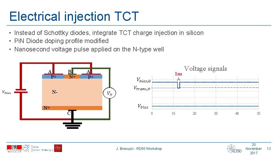
Electrical injection TCT • Instead of Schottky diodes, integrate TCT charge injection in silicon • Pi. N Diode doping profile modified • Nanosecond voltage pulse applied on the N-type well A P+ B N+ N+ 1 ns Voltage signals N- A P+ C 0 J. Bronuzzi - RD 50 Workshop 10 20 30 40 50 20 November 2017 13
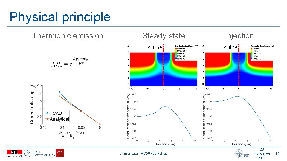
Physical principle Thermionic emission Steady state cutline Injection cutline J. Bronuzzi - RD 50 Workshop 20 November 2017 14
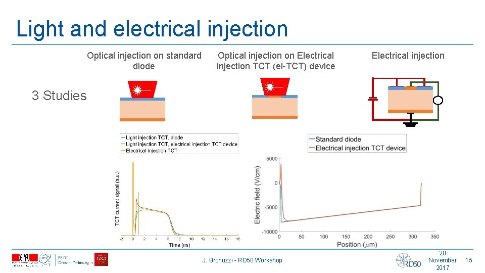
Light and electrical injection Optical injection on standard diode Optical injection on Electrical injection TCT (el-TCT) device Electrical injection 3 Studies J. Bronuzzi - RD 50 Workshop 20 November 2017 15
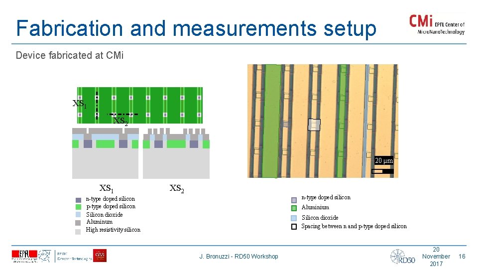
Fabrication and measurements setup Device fabricated at CMi XS 1 XS 2 20 µm XS 1 XS 2 n-type doped silicon p-type doped silicon Silicon dioxide Aluminum High resistivity silicon Aluminium Silicon dioxide Spacing between n and p-type doped silicon J. Bronuzzi - RD 50 Workshop 20 November 2017 16
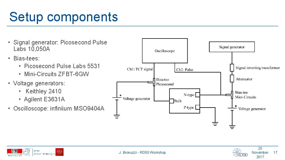
Setup components • Signal generator: Picosecond Pulse Labs 10, 050 A • Bias-tees: • Picosecond Pulse Labs 5531 • Mini-Circuits ZFBT-6 GW • Voltage generators: • Keithley 2410 • Agilent E 3631 A • Oscilloscope: infiniium MSO 9404 A J. Bronuzzi - RD 50 Workshop 20 November 2017 17
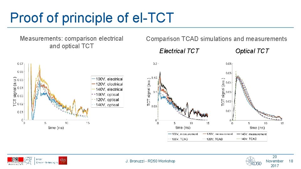
Proof of principle of el-TCT Measurements: comparison electrical and optical TCT Comparison TCAD simulations and measurements Electrical TCT J. Bronuzzi - RD 50 Workshop Optical TCT 20 November 2017 18
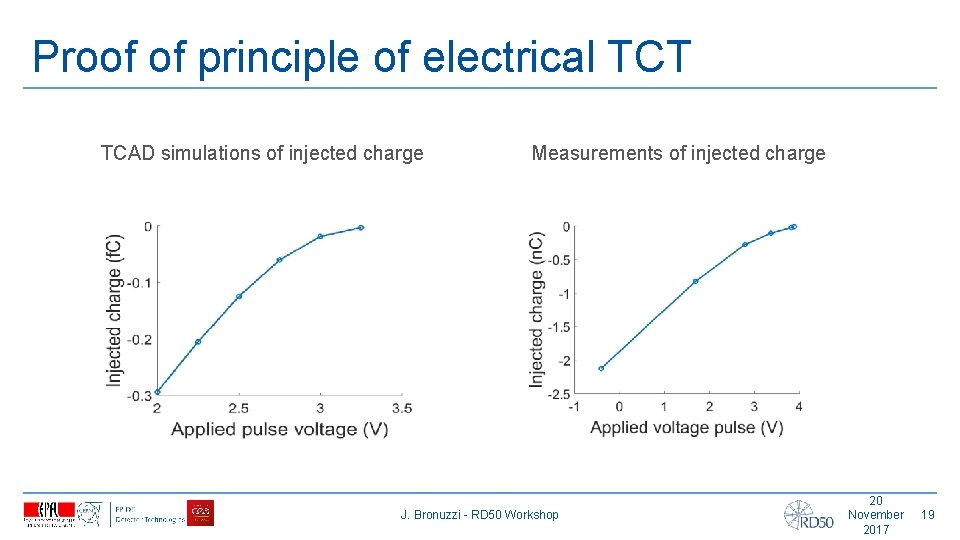
Proof of principle of electrical TCT TCAD simulations of injected charge Measurements of injected charge J. Bronuzzi - RD 50 Workshop 20 November 2017 19
Conclusions and outlook New manufacturing technique for monolithic silicon sensors is being investigated: • Characterization of bonding interface with TCT has been modeled • Fabrication of devices for TCT bonding interface characterization is in progress • Measurements will be performed at CERN in the early 2018 El-TCT has been developed: • The proof of principle has been demonstrated • Evaluation of el-TCT for online measurements of radiation induced damage in silicon samples at IRRAD proton facility in 2018 J. Bronuzzi - RD 50 Workshop 20 November 2017 20
Thank you for the attention Questions? J. Bronuzzi - RD 50 Workshop 20 November 2017 21
- Slides: 21