TCAD Simulation of irradiated Silicon radiation detector using

![Publications [1] M. Benoit, A. Lounis, and N. Dinu, “Simulation of charge multiplication and Publications [1] M. Benoit, A. Lounis, and N. Dinu, “Simulation of charge multiplication and](https://slidetodoc.com/presentation_image/2974204c244c30ffda699d3e6f071a6e/image-41.jpg)
- Slides: 46

TCAD Simulation of irradiated Silicon radiation detector using commercial simulation products Mathieu Benoit, CERN, PH-LCD 20 th RD 50 Workshop, May 31 st 2012 1

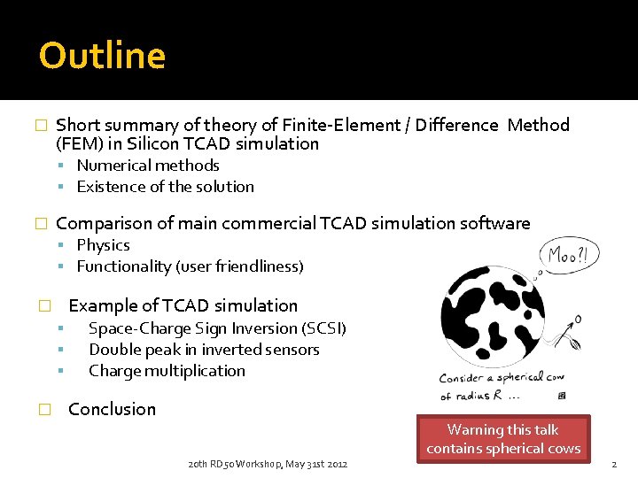
Outline � Short summary of theory of Finite-Element / Difference Method (FEM) in Silicon TCAD simulation Numerical methods Existence of the solution � Comparison of main commercial TCAD simulation software Physics Functionality (user friendliness) Example of TCAD simulation � � Space-Charge Sign Inversion (SCSI) Double peak in inverted sensors Charge multiplication Conclusion 20 th RD 50 Workshop, May 31 st 2012 Warning this talk contains spherical cows 2

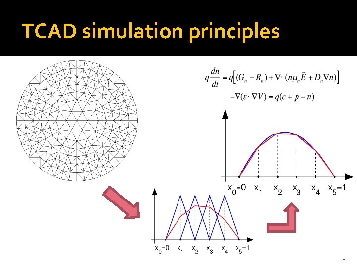
TCAD simulation principles 3

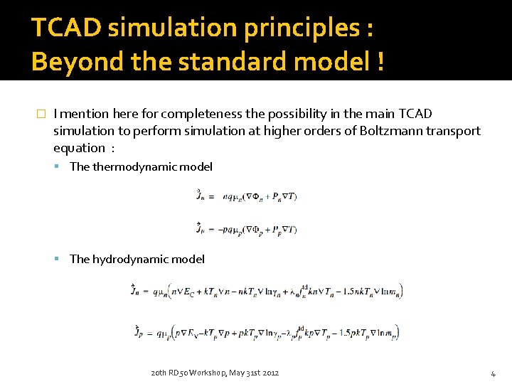
TCAD simulation principles : Beyond the standard model ! � I mention here for completeness the possibility in the main TCAD simulation to perform simulation at higher orders of Boltzmann transport equation : The thermodynamic model The hydrodynamic model 20 th RD 50 Workshop, May 31 st 2012 4

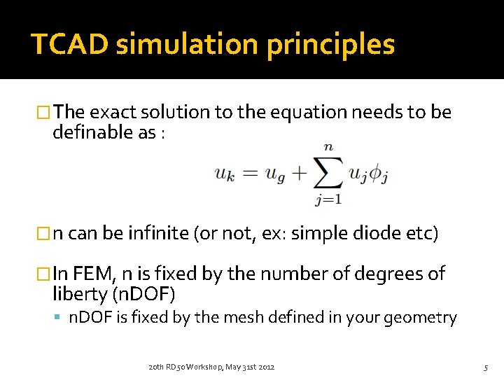
TCAD simulation principles �The exact solution to the equation needs to be definable as : �n can be infinite (or not, ex: simple diode etc) �In FEM, n is fixed by the number of degrees of liberty (n. DOF) n. DOF is fixed by the mesh defined in your geometry 20 th RD 50 Workshop, May 31 st 2012 5

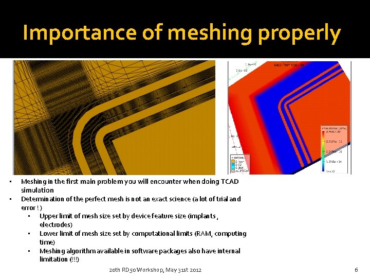
Importance of meshing properly • • Meshing in the first main problem you will encounter when doing TCAD simulation Determination of the perfect mesh is not an exact science (a lot of trial and error ! ) • Upper limit of mesh size set by device feature size (implants , electrodes) • Lower limit of mesh size set by computational limits (RAM, computing time) • Meshing algorithm available in software packages also have internal limitation (!!!) 20 th RD 50 Workshop, May 31 st 2012 6

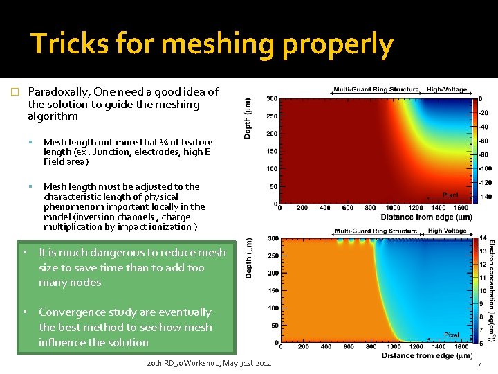
Tricks for meshing properly � Paradoxally, One need a good idea of the solution to guide the meshing algorithm Mesh length not more that ¼ of feature length (ex : Junction, electrodes, high E Field area) Mesh length must be adjusted to the characteristic length of physical phenom important locally in the model (inversion channels , charge multiplication by impact ionization ) • It is much dangerous to reduce mesh size to save time than to add too many nodes • Convergence study are eventually the best method to see how mesh influence the solution 20 th RD 50 Workshop, May 31 st 2012 7

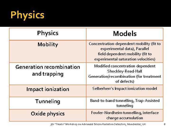
Physics Models Mobility Concentration-dependent mobility (fit to experimental data), Parallel field dependent mobility (fit to experimental saturation velocities) Generation recombination and trapping Modified concentration dependent Shockley-Read-Hall Generation/recombination (for treatment of defects) Impact ionization Selberherr’s Impact ionization model Tunneling Band-to-band tunnelling, Trap-Assisted tunneling Oxide physics Fowler-Nordheim tunnelling, interface charge accumulation 5 th "Trento" Workshop on Advanced Silicon Radiation Detectors, Manchester, UK 8

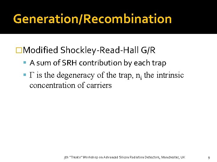
Generation/Recombination �Modified Shockley-Read-Hall G/R A sum of SRH contribution by each trap Γ is the degeneracy of the trap, ni the intrinsic concentration of carriers 5 th "Trento" Workshop on Advanced Silicon Radiation Detectors, Manchester, UK 9

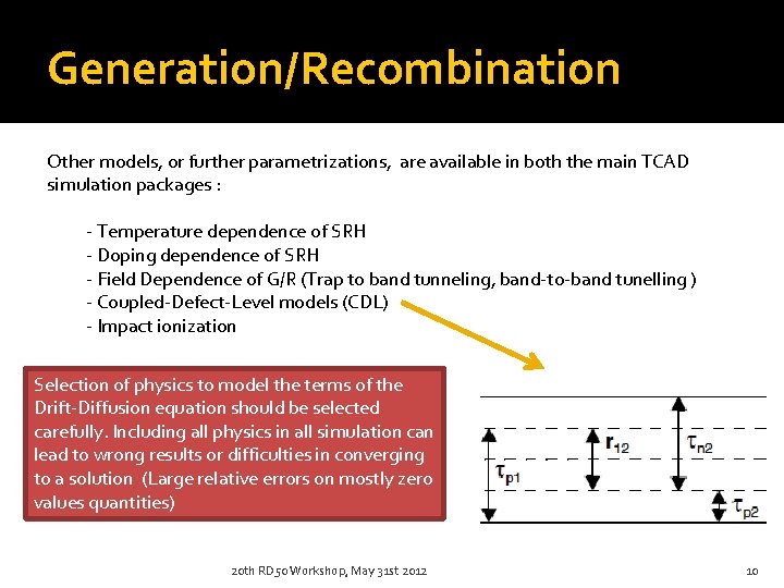
Generation/Recombination Other models, or further parametrizations, are available in both the main TCAD simulation packages : - Temperature dependence of SRH - Doping dependence of SRH - Field Dependence of G/R (Trap to band tunneling, band-to-band tunelling ) - Coupled-Defect-Level models (CDL) - Impact ionization Selection of physics to model the terms of the Drift-Diffusion equation should be selected carefully. Including all physics in all simulation can lead to wrong results or difficulties in converging to a solution (Large relative errors on mostly zero values quantities) 20 th RD 50 Workshop, May 31 st 2012 10

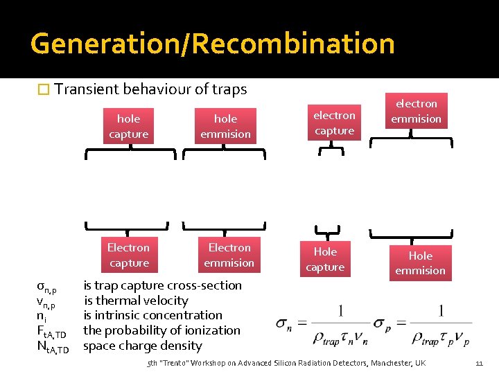
Generation/Recombination � Transient behaviour of traps hole capture Electron capture σn, p vn, p ni Ft. A, TD Nt. A, TD hole emmision Electron emmision is trap capture cross-section is thermal velocity is intrinsic concentration the probability of ionization space charge density electron capture Hole capture electron emmision Hole emmision 5 th "Trento" Workshop on Advanced Silicon Radiation Detectors, Manchester, UK 11

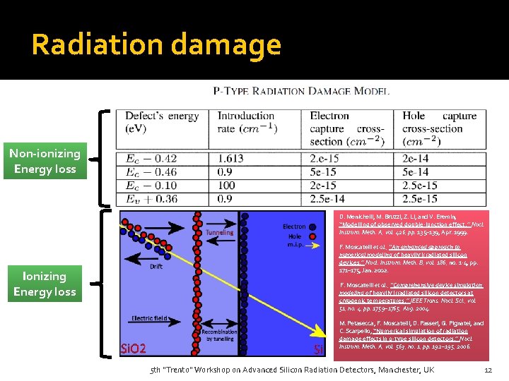
Radiation damage Non-ionizing Energy loss D. Menichelli, M. Bruzzi, Z. Li, and V. Eremin, “Modelling of observed double-junction effect, ” Nucl. Instrum. Meth. A, vol. 426, pp. 135– 139, Apr. 1999. Ionizing Energy loss F. Moscatelli et al. , “An enhanced approach to numerical modeling of heavily irradiated silicon devices, ” Nucl. Instrum. Meth. B, vol. 186, no. 1 -4, pp. 171– 175, Jan. 2002. F. Moscatelli et al. , “Comprehensive device simulation modeling of heavily irradiated silicon detectors at cryogenic temperatures, ” IEEE Trans. Nucl. Sci. , vol. 51, no. 4, pp. 1759– 1765, Aug. 2004. M. Petasecca, F. Moscatelli, D. Passeri, G. Pignatel, and C. Scarpello, “Numerical simulation of radiation damage effects in p-type silicon detectors, ” Nucl. Instrum. Meth. A, vol. 563, no. 1, pp. 192– 195, 2006. 5 th "Trento" Workshop on Advanced Silicon Radiation Detectors, Manchester, UK 12

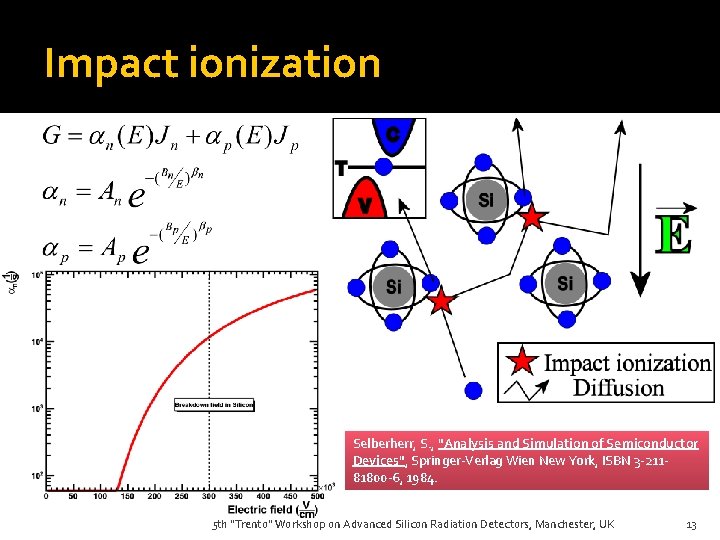
Impact ionization Selberherr, S. , "Analysis and Simulation of Semiconductor Devices", Springer-Verlag Wien New York, ISBN 3 -21181800 -6, 1984. 5 th "Trento" Workshop on Advanced Silicon Radiation Detectors, Manchester, UK 13

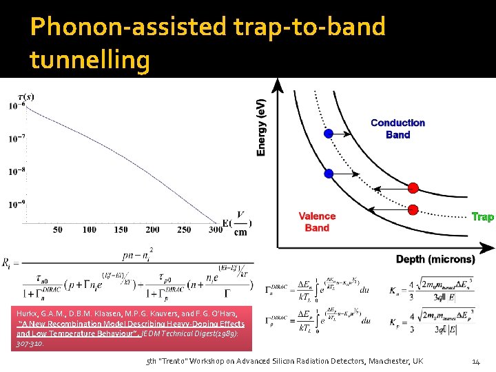
Phonon-assisted trap-to-band tunnelling Hurkx, G. A. M. , D. B. M. Klaasen, M. P. G. Knuvers, and F. G. O’Hara, “A New Recombination Model Describing Heavy-Doping Effects and Low Temperature Behaviour”, IEDM Technical Digest(1989): 307 -310. 5 th "Trento" Workshop on Advanced Silicon Radiation Detectors, Manchester, UK 14

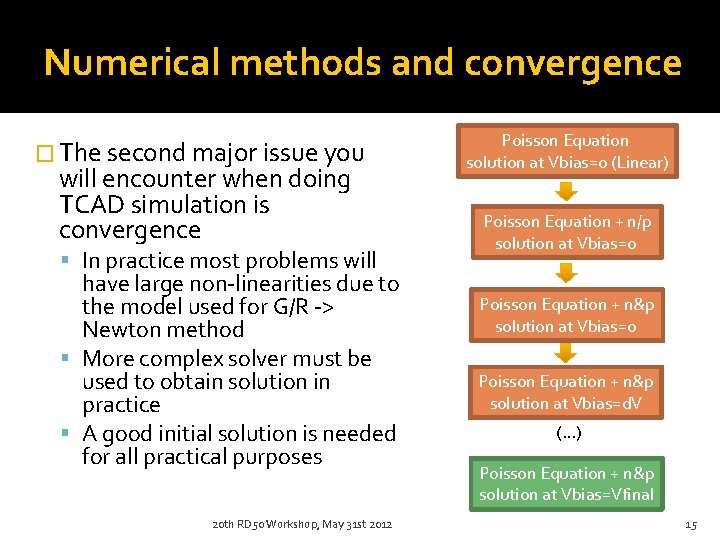
Numerical methods and convergence � The second major issue you will encounter when doing TCAD simulation is convergence In practice most problems will have large non-linearities due to the model used for G/R -> Newton method More complex solver must be used to obtain solution in practice A good initial solution is needed for all practical purposes 20 th RD 50 Workshop, May 31 st 2012 Poisson Equation solution at Vbias=0 (Linear) Poisson Equation + n/p solution at Vbias=0 Poisson Equation + n&p solution at Vbias=d. V (…) Poisson Equation + n&p solution at Vbias=Vfinal 15

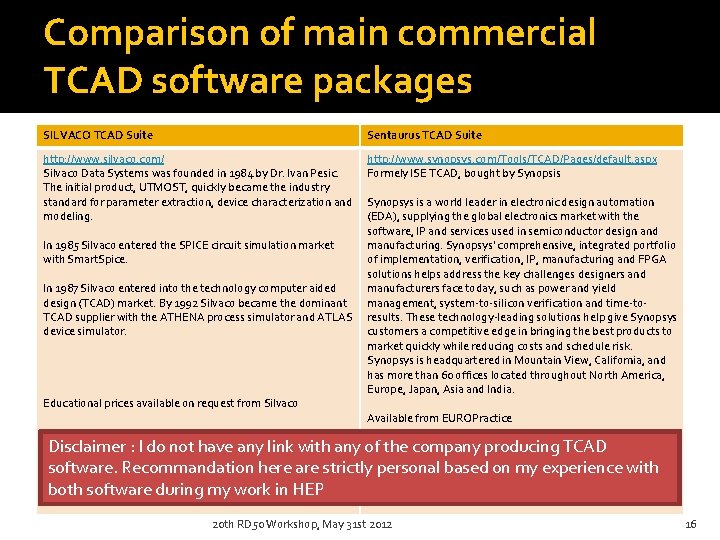
Comparison of main commercial TCAD software packages SILVACO TCAD Suite Sentaurus TCAD Suite http: //www. silvaco. com/ Silvaco Data Systems was founded in 1984 by Dr. Ivan Pesic. The initial product, UTMOST, quickly became the industry standard for parameter extraction, device characterization and modeling. http: //www. synopsys. com/Tools/TCAD/Pages/default. aspx Formely ISE TCAD, bought by Synopsis In 1985 Silvaco entered the SPICE circuit simulation market with Smart. Spice. In 1987 Silvaco entered into the technology computer aided design (TCAD) market. By 1992 Silvaco became the dominant TCAD supplier with the ATHENA process simulator and ATLAS device simulator. Educational prices available on request from Silvaco Synopsys is a world leader in electronic design automation (EDA), supplying the global electronics market with the software, IP and services used in semiconductor design and manufacturing. Synopsys' comprehensive, integrated portfolio of implementation, verification, IP, manufacturing and FPGA solutions helps address the key challenges designers and manufacturers face today, such as power and yield management, system-to-silicon verification and time-toresults. These technology-leading solutions help give Synopsys customers a competitive edge in bringing the best products to market quickly while reducing costs and schedule risk. Synopsys is headquartered in Mountain View, California, and has more than 60 offices located throughout North America, Europe, Japan, Asia and India. Available from EUROPractice Disclaimer : I do not have any link with any of the company producing TCAD software. Recommandation here are strictly personal based on my experience with both software during my work in HEP 20 th RD 50 Workshop, May 31 st 2012 16

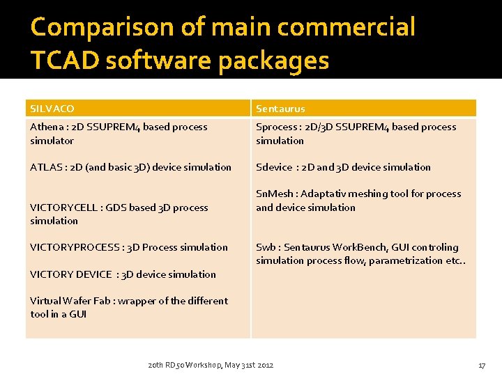
Comparison of main commercial TCAD software packages SILVACO Sentaurus Athena : 2 D SSUPREM 4 based process simulator Sprocess : 2 D/3 D SSUPREM 4 based process simulation ATLAS : 2 D (and basic 3 D) device simulation Sdevice : 2 D and 3 D device simulation VICTORYCELL : GDS based 3 D process simulation VICTORYPROCESS : 3 D Process simulation VICTORY DEVICE : 3 D device simulation Sn. Mesh : Adaptativ meshing tool for process and device simulation Swb : Sentaurus Work. Bench, GUI controling simulation process flow, parametrization etc. . Virtual Wafer Fab : wrapper of the different tool in a GUI 20 th RD 50 Workshop, May 31 st 2012 17

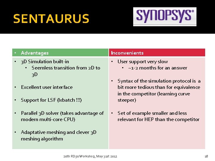
SENTAURUS • Advantages Inconvenients • 3 D Simulation built-in • Seemless transition from 2 D to 3 D • User support very slow • ~1 -2 months for an answer • Support for LSF (lxbatch !!!) • Syntax of the simulation protocol is a bit more tedious than for equivalence in the competitor (learning curve steeper) • Parallel 3 D solver (takes advantage of modern multi-core CPU) • Set of example smaller and less relevant for HEP than the competitor • Excellent user interface • Adaptative meshing and clever 3 D meshing algorithm 20 th RD 50 Workshop, May 31 st 2012 18

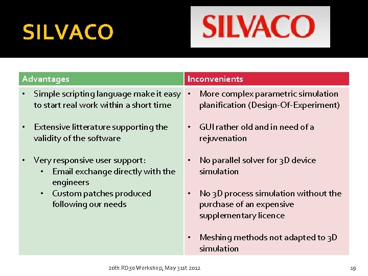
SILVACO Advantages Inconvenients • Simple scripting language make it easy • More complex parametric simulation to start real work within a short time planification (Design-Of-Experiment) • Extensive litterature supporting the validity of the software • GUI rather old and in need of a rejuvenation • Very responsive user support: • Email exchange directly with the engineers • Custom patches produced following our needs • No parallel solver for 3 D device simulation • No 3 D process simulation without the purchase of an expensive supplementary licence • Meshing methods not adapted to 3 D simulation 20 th RD 50 Workshop, May 31 st 2012 19

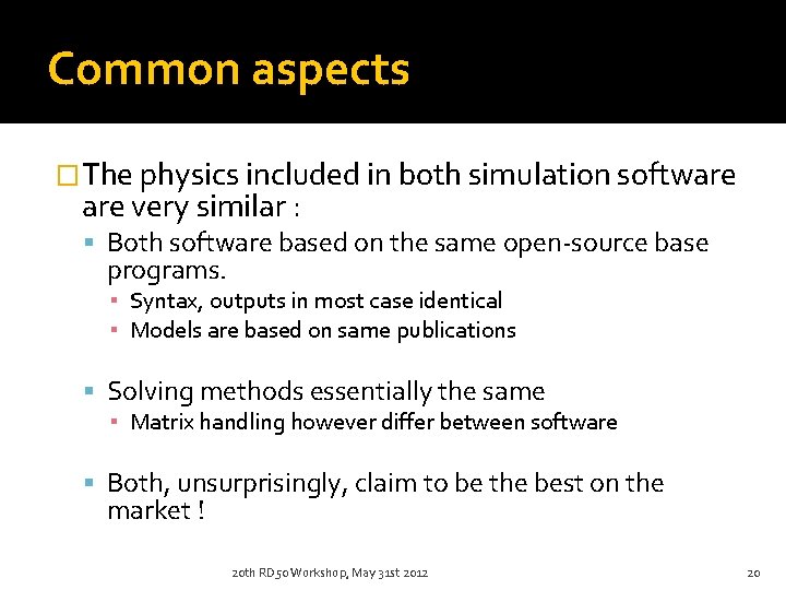
Common aspects �The physics included in both simulation software very similar : Both software based on the same open-source base programs. ▪ Syntax, outputs in most case identical ▪ Models are based on same publications Solving methods essentially the same ▪ Matrix handling however differ between software Both, unsurprisingly, claim to be the best on the market ! 20 th RD 50 Workshop, May 31 st 2012 20

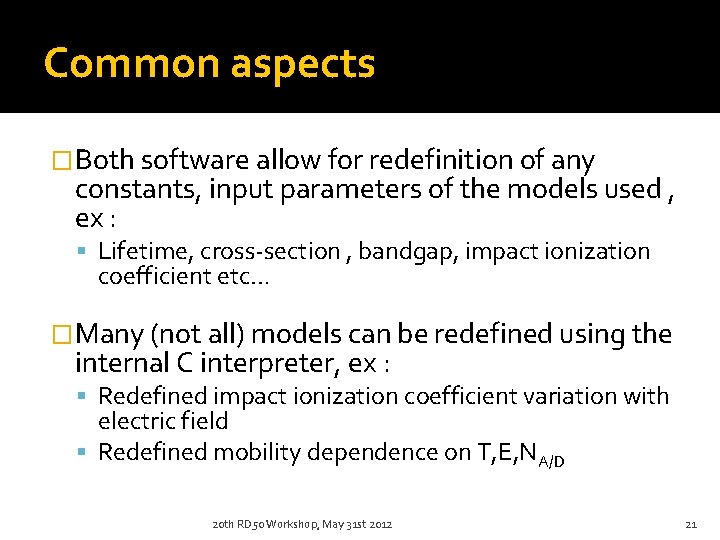
Common aspects �Both software allow for redefinition of any constants, input parameters of the models used , ex : Lifetime, cross-section , bandgap, impact ionization coefficient etc… �Many (not all) models can be redefined using the internal C interpreter, ex : Redefined impact ionization coefficient variation with electric field Redefined mobility dependence on T, E, NA/D 20 th RD 50 Workshop, May 31 st 2012 21

TCAD simulation as a black box (1) �Both software sold as compiled software with no access to source code, however : Both software extensively used in the industry with a lot of success translating in a major contribution to the improvement of the microelectronics Both software extensively documented with references provided : ▪ SILVACO ATLAS Manual -> 898 pages ▪ SENTAURUS DEVICE Manual -> 1284 pages 20 th RD 50 Workshop, May 31 st 2012 22

TCAD simulation as a black box (2) �The benefit of using a commercial software w. r. t Home-Made solution are : to benefit from a large user base (debugging, feedback and new features) Less focus on mathematics and coding more focus on physics (physicist can’t do everything, we should stick to what we know best ! ) ▪ Ex: Writing a Navier-Stokes solver for a 2 D very specific geometry (given a receipe and all equation and numerical methods) ~ 1 -2 months for a master student 20 th RD 50 Workshop, May 31 st 2012 23

TCAD simulation as a black box (3) � FEM is commonly use to provide reliable simulation for design of the plane that flew you here , or the cooling system of your laptop � Simulation of non-irradiated semiconductor device has reached a similar level or reliability � A lot of work from the RD 50 collaboration could very much bring the simulation of irradiated sensors to the same stat ! 20 th RD 50 Workshop, May 31 st 2012 24

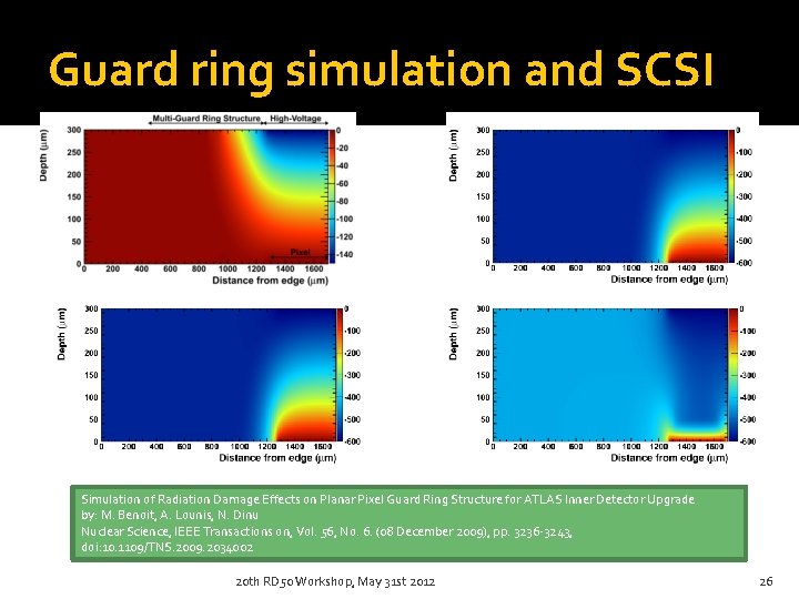
TCAD Simulation capabilities �TCAD is suitable for simulation of complex structure Guard rings , punch-trough E-Field distribution in presence of complex doping profiles �Transient simulation Apply a stress to a DC-Stable system and relax it back to equilibrium (ie. Virtual TCT) �AC Analysis (CV Curves, inter-pixel/strip capacitance) 20 th RD 50 Workshop, May 31 st 2012 25

Guard ring simulation and SCSI Simulation of Radiation Damage Effects on Planar Pixel Guard Ring Structure for ATLAS Inner Detector Upgrade by: M. Benoit, A. Lounis, N. Dinu Nuclear Science, IEEE Transactions on, Vol. 56, No. 6. (08 December 2009), pp. 3236 -3243, doi: 10. 1109/TNS. 2009. 2034002 20 th RD 50 Workshop, May 31 st 2012 26

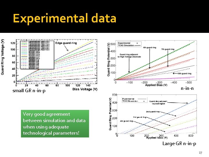
Experimental data small GR n-in-p n-in-n Very good agreement between simulation and data when using adequate technological parameters! Large GR n-in-p 27

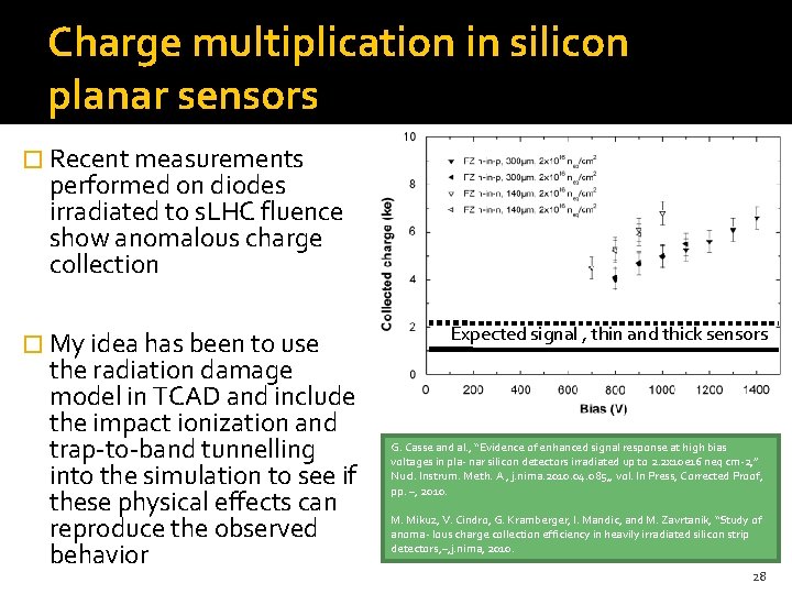
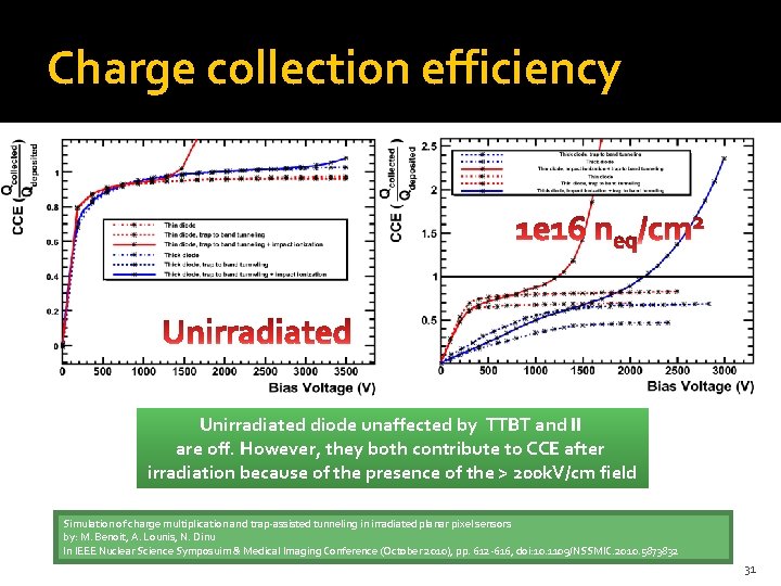
Charge multiplication in silicon planar sensors � Recent measurements performed on diodes irradiated to s. LHC fluence show anomalous charge collection � My idea has been to use the radiation damage model in TCAD and include the impact ionization and trap-to-band tunnelling into the simulation to see if these physical effects can reproduce the observed behavior Expected signal , thin and thick sensors G. Casse and al. , “Evidence of enhanced signal response at high bias voltages in pla- nar silicon detectors irradiated up to 2. 2 x 10 e 16 neq cm-2, ” Nucl. Instrum. Meth. A , j. nima. 2010. 04. 085, , vol. In Press, Corrected Proof, pp. –, 2010. M. Mikuz, V. Cindro, G. Kramberger, I. Mandic, and M. Zavrtanik, “Study of anoma- lous charge collection efficiency in heavily irradiated silicon strip detectors, –, j. nima, 2010. 28

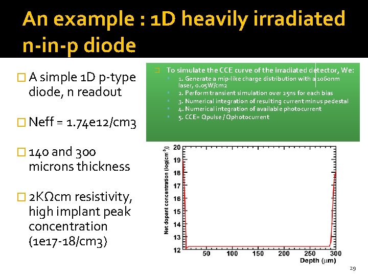
An example : 1 D heavily irradiated n-in-p diode � A simple 1 D p-type diode, n readout � Neff = 1. 74 e 12/cm 3 � To simulate the CCE curve of the irradiated detector, We: 1. Generate a mip-like charge distribution with a 1060 nm laser, 0. 05 W/cm 2 2. Perform transient simulation over 25 ns for each bias 3. Numerical integration of resulting current minus pedestal 4. Numerical integration of available photocurrent 5. CCE= Qpulse / Qphotocurrent � 140 and 300 microns thickness � 2 KΩcm resistivity, high implant peak concentration (1 e 17 -18/cm 3) 29

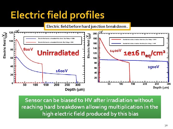
Electric field profiles Electric field before hard junction breakdown. 800 V 1400 V 1600 V 2500 V Sensor can be biased to HV after irradiation without reaching hard breakdown allowing multiplication in the high electric field produced by this bias 30

Charge collection efficiency Unirradiated diode unaffected by TTBT and II are off. However, they both contribute to CCE after irradiation because of the presence of the > 200 k. V/cm field Simulation of charge multiplication and trap-assisted tunneling in irradiated planar pixel sensors by: M. Benoit, A. Lounis, N. Dinu In IEEE Nuclear Science Symposuim & Medical Imaging Conference (October 2010), pp. 612 -616, doi: 10. 1109/NSSMIC. 2010. 5873832 31

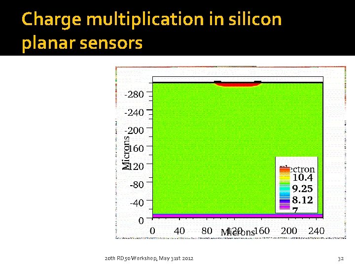
Charge multiplication in silicon planar sensors 20 th RD 50 Workshop, May 31 st 2012 32

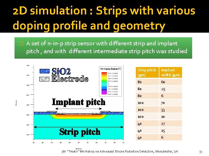
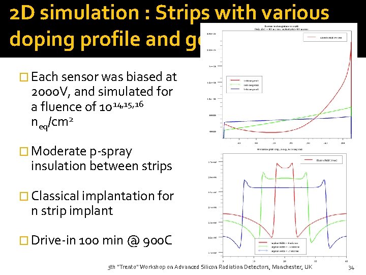
2 D simulation : Strips with various doping profile and geometry � A set of n-in-p strip sensor with different strip and implant pitch , and with different intermediate strip pitch was studied Strip pitch (mm) Implant width (mm) 80 60 80 25 80 6 100 70 100 33 100 10 40 27 40 15 40 6 5 th "Trento" Workshop on Advanced Silicon Radiation Detectors, Manchester, UK 33

2 D simulation : Strips with various doping profile and geometry � Each sensor was biased at 2000 V, and simulated for a fluence of 1014, 15, 16 neq/cm 2 � Moderate p-spray insulation between strips � Classical implantation for n strip implant � Drive-in 100 min @ 900 C 5 th "Trento" Workshop on Advanced Silicon Radiation Detectors, Manchester, UK 34

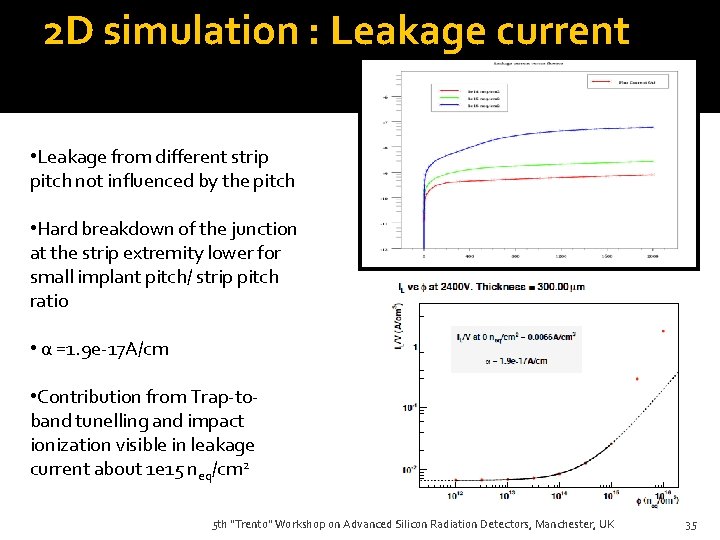
2 D simulation : Leakage current • Leakage from different strip pitch not influenced by the pitch • Hard breakdown of the junction at the strip extremity lower for small implant pitch/ strip pitch ratio • α =1. 9 e-17 A/cm • Contribution from Trap-toband tunelling and impact ionization visible in leakage current about 1 e 15 neq/cm 2 5 th "Trento" Workshop on Advanced Silicon Radiation Detectors, Manchester, UK 35

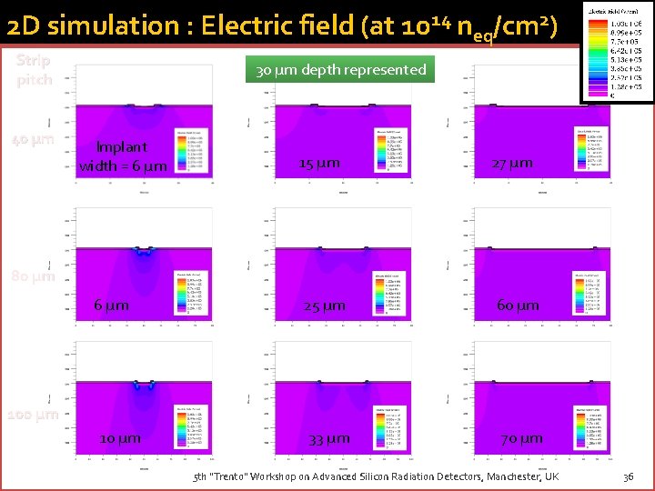
2 D simulation : Electric field (at 1014 neq/cm 2) Strip pitch 40 µm 30 µm depth represented Implant width = 6 µm 15 µm 27 µm 80 µm 6 µm 25 µm 60 µm 33 µm 70 µm 10 µm 5 th "Trento" Workshop on Advanced Silicon Radiation Detectors, Manchester, UK 36

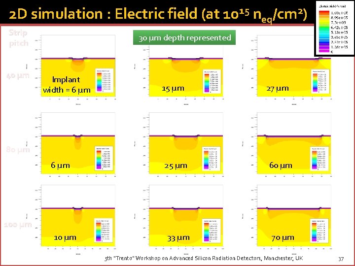
2 D simulation : Electric field (at 1015 neq/cm 2) Strip pitch 40 µm 30 µm depth represented Implant width = 6 µm 15 µm 27 µm 80 µm 6 µm 25 µm 60 µm 33 µm 70 µm 10 µm 5 th "Trento" Workshop on Advanced Silicon Radiation Detectors, Manchester, UK 37

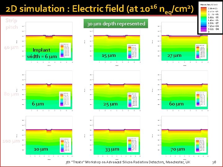
2 D simulation : Electric field (at 1016 neq/cm 2) Strip pitch 40 µm 30 µm depth represented Implant width = 6 µm 15 µm 27 µm 80 µm 6 µm 25 µm 60 µm 33 µm 70 µm 10 µm 5 th "Trento" Workshop on Advanced Silicon Radiation Detectors, Manchester, UK 38

From measurements to prediction � TCAD softwares offer a large parameter space to fit RD 50 measurements � Optimization packages are available within the software to fit data to simulation by varying a few parameters � Knowing well the characteristics of the simulated structures is very helpful to produce quantitative results Doping/Active dopant profile Mask design and processing parameters 20 th RD 50 Workshop, May 31 st 2012 39

Conclusion � TCAD simulation proves to be a powerful tool for studying the behavior of rather complex semiconductor structure Qualitative results reproducing main aspects of radiation damage can be performed easily Further work with test structure and extensive characterization is needed to produce more quantitative results � Commercial TCAD software mature products that have proven the usefulness Large user base Fast, well coded software, ready to use by a non-programmer Careful and detailed tuning of radiation damage model by the RD 50 collaboration would be a wonderful addition to the TCAD toolbox Thank you ! 20 th RD 50 Workshop, May 31 st 2012 40
![Publications 1 M Benoit A Lounis and N Dinu Simulation of charge multiplication and Publications [1] M. Benoit, A. Lounis, and N. Dinu, “Simulation of charge multiplication and](https://slidetodoc.com/presentation_image/2974204c244c30ffda699d3e6f071a6e/image-41.jpg)
Publications [1] M. Benoit, A. Lounis, and N. Dinu, “Simulation of charge multiplication and trap-assisted tunneling in irradiated planar pixel sensors, ” in IEEE Nuclear Science Symposuim & Medical Imaging Conference. IEEE, Oct. 2010, pp. 612– 616. [Online]. Available: http: //dx. doi. org/10. 1109/NSSMIC. 2010. 5873832 [6] ——, “Simulation of radiation damage effects on planar pixel guard ring structure for ATLAS inner detector upgrade, ” Nuclear Science, IEEE Transactions on, vol. 56, no. 6, pp. 3236– 3243, Dec. 2009. [Online]. Available: http: //dx. doi. org/10. 1109/TNS. 2009. 2034002 [2] J. Weingarten, S. Altenheiner, M. Beimforde, M. Benoit, M. Bomben, G. Calderini, C. Gallrapp, M. George, S. Gibson, S. Grinstein, Z. Janoska, J. Jentzsch, O. Jinnouchi, T. Kishida, A. La Rosa, V. Libov, A. Macchiolo, G. Marchiori, D. Mu nstermann, R. Nagai, G. Piacquadio, B. Ristic, I. Rubinskiy, A. Rummler, Y. Takubo, G. Troska, S. Tsiskaridtze, I. Tsurin, Y. Unno, P. Weigel, and T. Wittig, “Planar pixel sensors for the ATLAS upgrade: Beam tests results, ” Apr. 2012. [Online]. Available: http: //arxiv. org/abs/1204. 1266 [7] L. A. Hamel, M. Benoit, B. Donmez, J. R. Macri, M. L. Mc. Connell, T. Narita, and J. M. Ryan, “Optimization of Single-Sided Charge-Sharing strip detectors, ” in Nuclear Science Symposium Conference Record, 2006. IEEE, vol. 6, Nov. 2006, pp. 3759– 3761. [Online]. Available: http: //dx. doi. org/10. 1109/NSSMIC. 2006. 353811 [3] M. Benoit, J. Ma rk, P. Weiss, D. Benoit, J. C. Clemens, D. Fougeron, B. Janvier, M. Jevaud, S. Karkar, M. Menouni, F. Pain, L. Pinot, C. Morel, and P. Laniece, “New concept of a submillimetric pixellated silicon detector for intracerebral application, ” Nuclear Instruments and Methods in Physics Research Section A: Accelerators, Spectrometers, Detectors and Associated Equipment, Aug. 2011. [Online]. Available: http: //dx. doi. org/10. 1016/j. nima. 2011. 08. 027 [4] G. Calderini, M. Benoit, N. Dinu, A. Lounis, and G. Marchiori, “Simulations of planar pixel sensors for the ATLAS high luminosity upgrade, ” Nuclear Instruments and Methods in Physics Research Section A: Accelerators, Spectrometers, Detectors and Associated Equipment, Apr. 2010. [Online]. Available: http: //dx. doi. org/10. 1016/j. nima. 2010. 04. 082 [8] A. Lounis, D. Martinot, G. Calderini, G. Marchiori, M. Benoit, and N. Dinu, “TCAD simulations of ATLAS pixel guard ring and edge structure for SLHC upgrade, ” CERN, Geneva, Tech. Rep. ATL-COM-UPGRADE-2009 -013, Oct. 2009. [9] M. Benoit and L. A. Hamel, “Simulation of charge collection processes in semiconductor Cd. Zn. Te -ray detectors, ” Nuclear Instruments and Methods in Physics Research Section A: Accelerators, Spectrometers, Detectors and Associated Equipment, vol. 606, no. 3, pp. 508– 516, Jul. 2009. [Online]. Available: http: //dx. doi. org/10. 1016/j. nima. 2009. 04. 019 [10] M. Benoit, A. Lounis, and N. Dinu, “Simulation of guard ring influence on the performance of ATLAS pixel detectors for inner layer replacement, ” J. Inst. , vol. 4, no. 03, 2009. [Online]. Available: http: //www. iop. org/EJ/abstract/search=66292014. 1/1748 -0221/4/03/P 03025 [5] M. Benoit, A. Lounis, and N. Dinu, “Simulation of charge multiplication and trap-assisted tunneling in irradiated planar pixel sensors, ” CERN, Geneva, Tech. Rep. ATL-UPGRADE-INT-2010 -002, Oct. 2010. Thesis (in english) : Étude des détecteurs planaires pixels durcis aux radiations pour la mise à jour du détecteur de vertex d'ATLAS 20 th RD 50 Workshop, May 31 st 2012 41

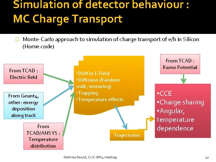
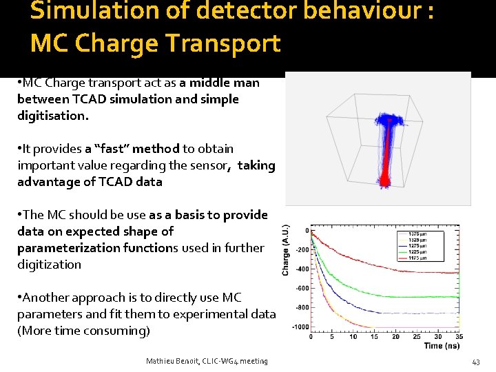
Simulation of detector behaviour : MC Charge Transport � Monte-Carlo approach to simulation of charge transport of e/h in Silicon (Home code) From TCAD : Electric field From Geant 4, other: energy deposition along track From TCAD/ANSYS : Temperature distribution • Drift in E Field • Diffusion (Random walk, smearing) • Trapping • Temperature effects Trajectories Mathieu Benoit, CLIC-WG 4 meeting From TCAD : Ramo Potential • CCE • Charge sharing • Angular, temperature dependence 42

Simulation of detector behaviour : MC Charge Transport • MC Charge transport act as a middle man between TCAD simulation and simple digitisation. • It provides a “fast” method to obtain important value regarding the sensor, taking advantage of TCAD data • The MC should be use as a basis to provide data on expected shape of parameterization functions used in further digitization • Another approach is to directly use MC parameters and fit them to experimental data (More time consuming) Mathieu Benoit, CLIC-WG 4 meeting 43

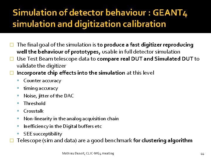
Simulation of detector behaviour : GEANT 4 simulation and digitization calibration The final goal of the simulation is to produce a fast digitizer reproducing well the behaviour of prototypes, usable in full detector simulation � Use Test Beam telescope data to compare real DUT and Simulated DUT to validate the digitizer � Incorporate chip effects into the simulation at this level � Counter accuracy timing accuracy Noise, jitter of the DAC Threshold Crosstalk Non-linearity in the analog acquisition chain Inefficiency in the Digital buffers etc SEE succeptibility � Telescope (sim and data) are a good benchmark for clustering algorithm Mathieu Benoit, CLIC-WG 4 meeting 44

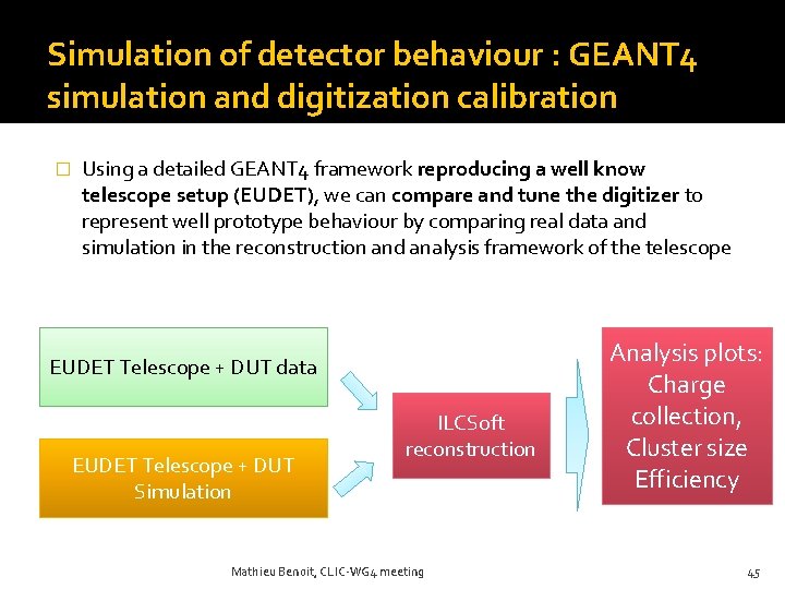
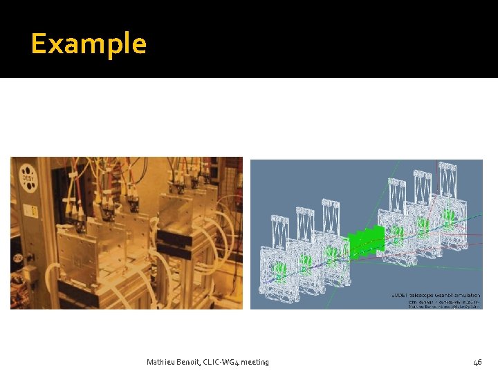
Simulation of detector behaviour : GEANT 4 simulation and digitization calibration � Using a detailed GEANT 4 framework reproducing a well know telescope setup (EUDET), we can compare and tune the digitizer to represent well prototype behaviour by comparing real data and simulation in the reconstruction and analysis framework of the telescope EUDET Telescope + DUT data EUDET Telescope + DUT Simulation ILCSoft reconstruction Mathieu Benoit, CLIC-WG 4 meeting Analysis plots: Charge collection, Cluster size Efficiency 45

Example Mathieu Benoit, CLIC-WG 4 meeting 46