TCAD Simulation of CCPD family of HVCMOS sensors

- Slides: 17

TCAD Simulation of CCPD family of HVCMOS sensors Mathieu Benoit FACULTÉ DES SCIENCES Section Physique

Outline • Topology of CCPD sensors – Well definition – Possible substrate resistivity • Study of parameters influencing of depletion in CCPD Sensors – Deep-N-Well and PSUB dimensions – Substrate Resistivity – Back-Side vs Front-Side biasing • Charge collection in CCPD sensors FACULTÉ DES SCIENCES Section Physique

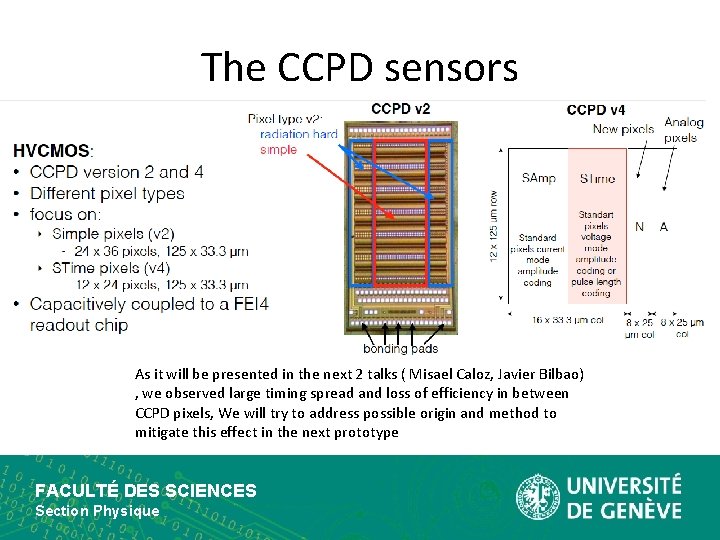
The CCPD sensors As it will be presented in the next 2 talks ( Misael Caloz, Javier Bilbao) , we observed large timing spread and loss of efficiency in between CCPD pixels, We will try to address possible origin and method to mitigate this effect in the next prototype FACULTÉ DES SCIENCES Section Physique

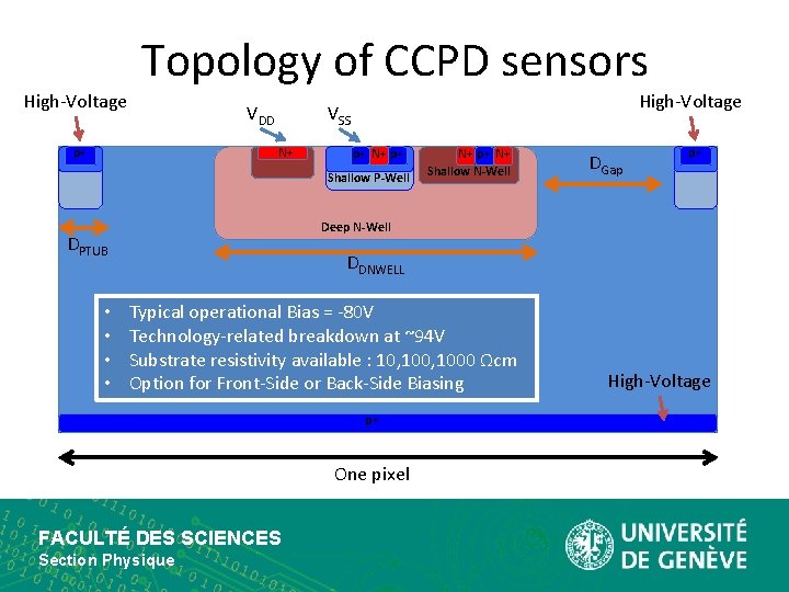
High-Voltage Topology of CCPD sensors VDD p+ High-Voltage VSS N+ p+ Shallow P-Well DGap p+ Deep N-Well DPTUB • • N+ p+ N+ Shallow N-Well DDNWELL Typical operational Bias = -80 V Technology-related breakdown at ~94 V Substrate resistivity available : 10, 1000 Ωcm Option for Front-Side or Back-Side Biasing p+ One pixel FACULTÉ DES SCIENCES Section Physique High-Voltage

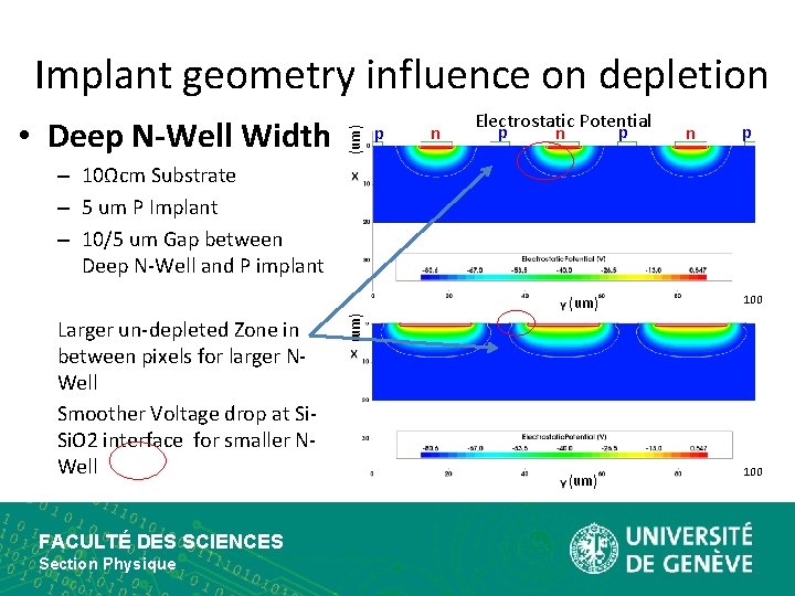
• Deep N-Well Width (um) Implant geometry influence on depletion p n Electrostatic Potential p p n n p – 10Ωcm Substrate – 5 um P Implant – 10/5 um Gap between Deep N-Well and P implant Larger un-depleted Zone in between pixels for larger NWell Smoother Voltage drop at Si. O 2 interface for smaller NWell FACULTÉ DES SCIENCES Section Physique 100 (um) 100

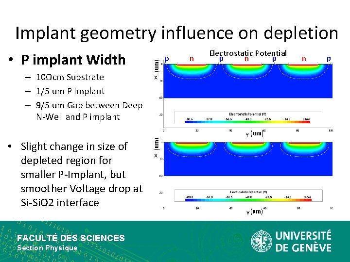
• P implant Width – 10Ωcm Substrate – 1/5 um P Implant – 9/5 um Gap between Deep N-Well and P implant (um) Implant geometry influence on depletion p n Electrostatic Potential p p n • Slight change in size of depleted region for smaller P-Implant, but smoother Voltage drop at Si-Si. O 2 interface FACULTÉ DES SCIENCES Section Physique (um) n p

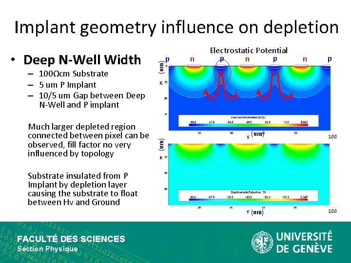
Implant geometry influence on depletion Much larger depleted region connected between pixel can be observed, fill factor no very influenced by topology (um) – 100Ωcm Substrate – 5 um P Implant – 10/5 um Gap between Deep N-Well and P implant p n n p (um) 100 (um) • Deep N-Well Width Electrostatic Potential p p n Substrate insulated from P Implant by depletion layer causing the substrate to float between Hv and Ground FACULTÉ DES SCIENCES Section Physique

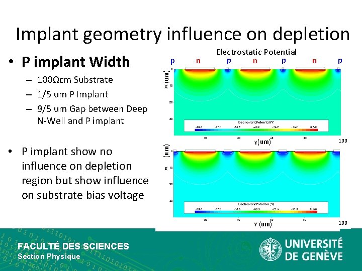
Implant geometry influence on depletion • P implant show no influence on depletion region but show influence on substrate bias voltage FACULTÉ DES SCIENCES Section Physique n n p (um) – 100Ωcm Substrate – 1/5 um P Implant – 9/5 um Gap between Deep N-Well and P implant p (um) • P implant Width Electrostatic Potential p p n (um) 100

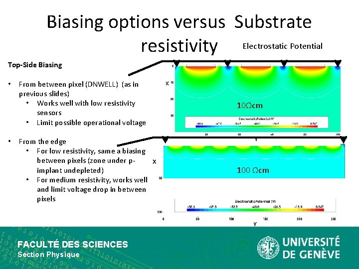
Biasing options versus Substrate resistivity Electrostatic Potential Top-Side Biasing • • From between pixel (DNWELL) (as in previous slides) • Works well with low resistivity sensors • Limit possible operational voltage 10Ωcm From the edge • For low resistivity, same a biasing between pixels (zone under pimplant undepleted) • For medium resistivity, works well and limit voltage drop in between pixels 100 Ωcm FACULTÉ DES SCIENCES Section Physique

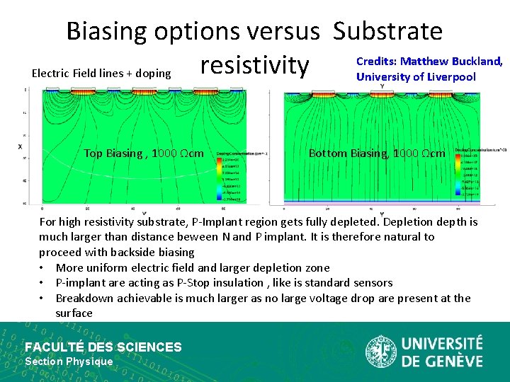
Biasing options versus Substrate Credits: Matthew Buckland, resistivity Electric Field lines + doping University of Liverpool Top Biasing , 1000 Ωcm Bottom Biasing, 1000 Ωcm For high resistivity substrate, P-Implant region gets fully depleted. Depletion depth is much larger than distance beween N and P implant. It is therefore natural to proceed with backside biasing • More uniform electric field and larger depletion zone • P-implant are acting as P-Stop insulation , like is standard sensors • Breakdown achievable is much larger as no large voltage drop are present at the surface FACULTÉ DES SCIENCES Section Physique

Charge Collection : Diffusion vs Drift • 10Ωcm substrate, • -80 V bias • Particle incident in the middle of the DNWell • 1 ns step displayed FACULTÉ DES SCIENCES Section Physique

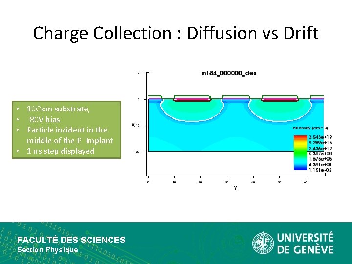
Charge Collection : Diffusion vs Drift • 10Ωcm substrate, • -80 V bias • Particle incident in the middle of the P Implant • 1 ns step displayed FACULTÉ DES SCIENCES Section Physique

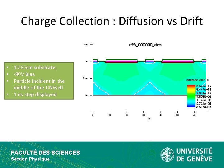
Charge Collection : Diffusion vs Drift • 100Ωcm substrate, • -80 V bias • Particle incident in the middle of the DNWell • 1 ns step displayed FACULTÉ DES SCIENCES Section Physique

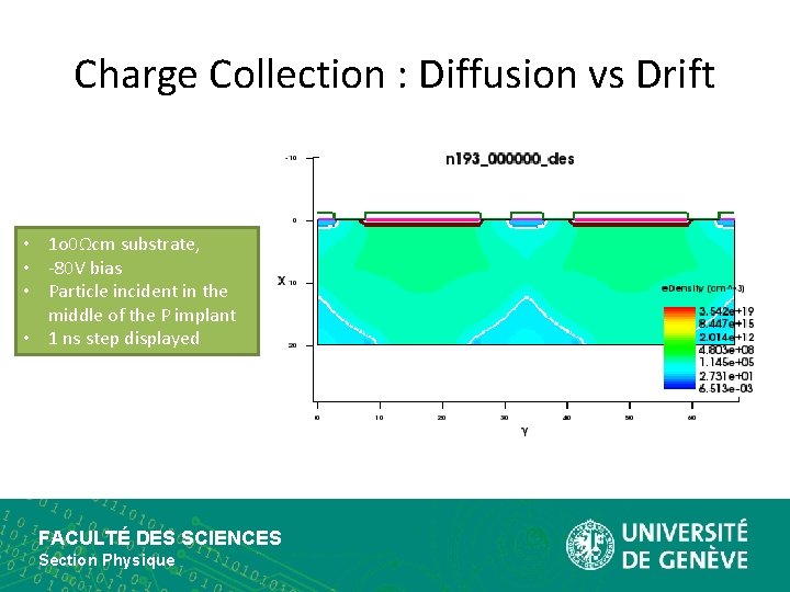
Charge Collection : Diffusion vs Drift • 1 o 0Ωcm substrate, • -80 V bias • Particle incident in the middle of the P implant • 1 ns step displayed FACULTÉ DES SCIENCES Section Physique

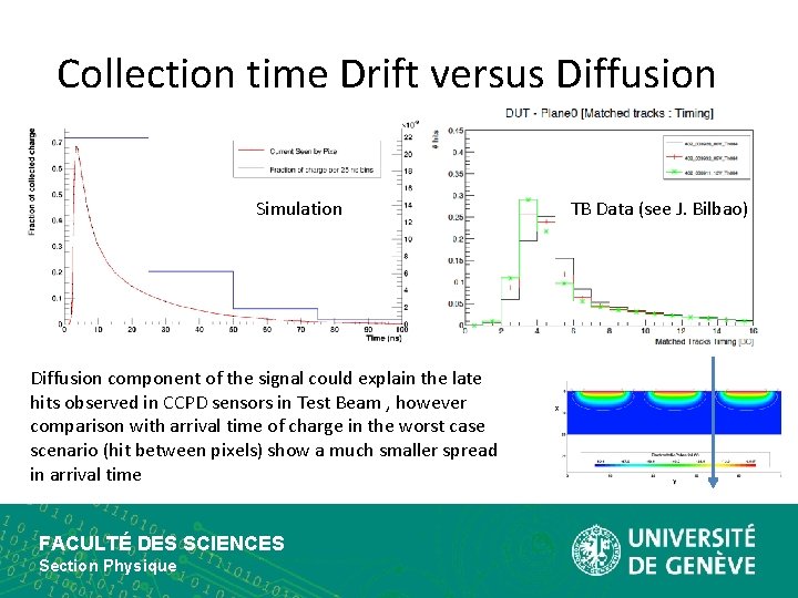
Collection time Drift versus Diffusion Simulation Diffusion component of the signal could explain the late hits observed in CCPD sensors in Test Beam , however comparison with arrival time of charge in the worst case scenario (hit between pixels) show a much smaller spread in arrival time FACULTÉ DES SCIENCES Section Physique TB Data (see J. Bilbao)

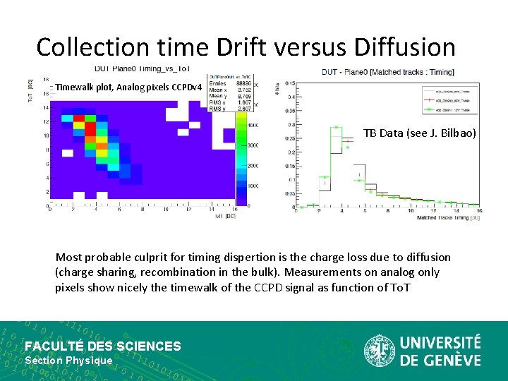
Collection time Drift versus Diffusion Timewalk plot, Analog pixels CCPDv 4 TB Data (see J. Bilbao) Most probable culprit for timing dispertion is the charge loss due to diffusion (charge sharing, recombination in the bulk). Measurements on analog only pixels show nicely the timewalk of the CCPD signal as function of To. T FACULTÉ DES SCIENCES Section Physique

Conclusion • TCAD Simulation of CCPD sensor geometry show clear influence of implant dimensions on depletion zone for low resistivity sensors • Must keep Deep N-Well as large as possible and P implant as small as possible, within the design rules • We evaluated all possible biasing options to choose the most suitable for most resistivity • Top-Side biasing or edge biasing most efficient for low to mid resistivity • When Depletion depth >> High Voltage to Ground electrode distance , backside biasing is preferred • Charge collection in low resistivity show clear contribution of diffusion in the region between pixels, contribution to charge collection loss and charge sharing • Small signal can be guilty for large time spread in experimental data FACULTÉ DES SCIENCES Section Physique Next … Laboratory characterization of CCPDv 2 and CCPDv 4 capacitive coupled to FEI 4, Misael Caloz SPS Test Beam characterization results with CCPDv 2 and CCPDv 4 capacitively-coupled to FEI 4, Javier Bilbao