TCAD Simulation and test setup For CMOS Pixel
![Background and motivation R [mm] Vertex Silicon Tracker Layout of CEPC vertex and Silicon Background and motivation R [mm] Vertex Silicon Tracker Layout of CEPC vertex and Silicon](https://slidetodoc.com/presentation_image_h2/b99ab26177aa2c8252982cee020e0a74/image-3.jpg)
- Slides: 13

TCAD Simulation and test setup For CMOS Pixel Sensor based on a 0. 18 μm technology 李龙 刘剑 张亮 董家宁 王萌 Shandong University longli@mail. sdu. edu. cn Hengyang , Oct. 16 th , 2018 2021/9/20 1

Outlines • Background and motivation • Brief introduction of TCAD simulation • CMOS Pixel Sensor simulation work based on a 0. 18 μm technology • Chip test for the sensor simulated • Summary 2021/9/20 2
![Background and motivation R mm Vertex Silicon Tracker Layout of CEPC vertex and Silicon Background and motivation R [mm] Vertex Silicon Tracker Layout of CEPC vertex and Silicon](https://slidetodoc.com/presentation_image_h2/b99ab26177aa2c8252982cee020e0a74/image-3.jpg)
Background and motivation R [mm] Vertex Silicon Tracker Layout of CEPC vertex and Silicon Tracker Z [mm] A Tower Jazz 0. 18μm technology is going to be applied on CEPC Silicon Tracker. In order to reach the spatial resolution of 7μm, the Charge Collection Efficiency and Diode capacitance which matter much in SNR should be simulated before chip design. This talk is about the simulation work and test setup for a CMOS Pixel Sensor based on Tower Jazz 0. 18 μm technology. 2021/9/20 3

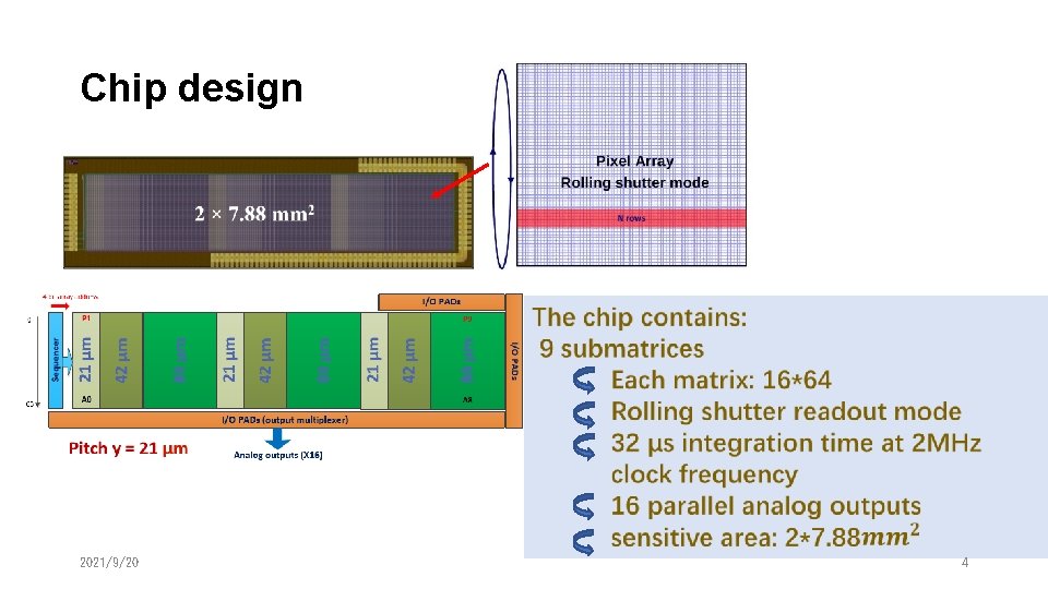
Chip design 2021/9/20 4

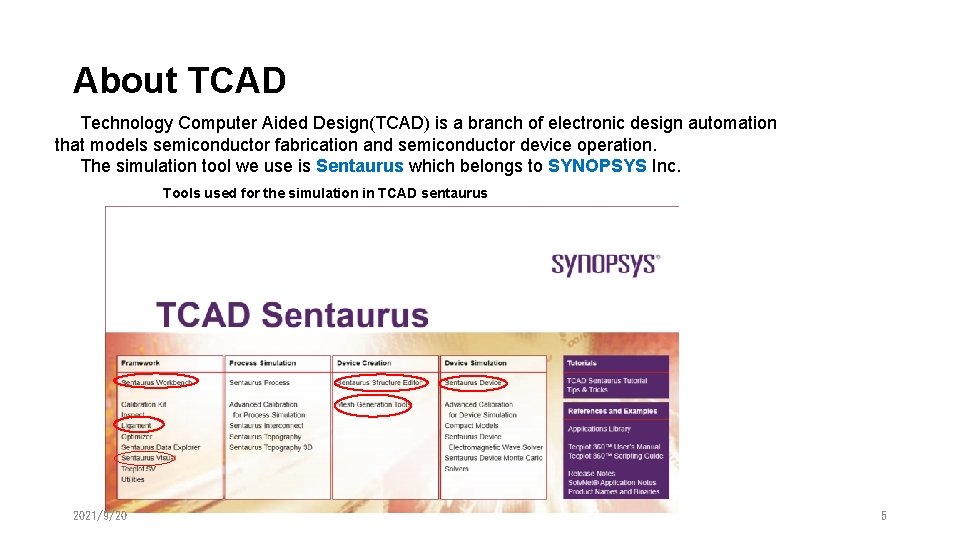
About TCAD Technology Computer Aided Design(TCAD) is a branch of electronic design automation that models semiconductor fabrication and semiconductor device operation. The simulation tool we use is Sentaurus which belongs to SYNOPSYS Inc. Tools used for the simulation in TCAD sentaurus 2021/9/20 5

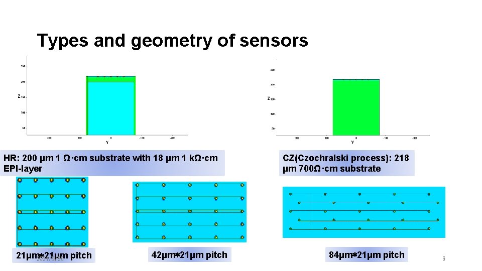
Types and geometry of sensors HR: 200 μm 1 Ω·cm substrate with 18 μm 1 kΩ·cm EPI-layer 21μm*21μm 2021/9/20 pitch 42μm*21μm pitch CZ(Czochralski process): 218 μm 700Ω·cm substrate 84μm*21μm pitch 6

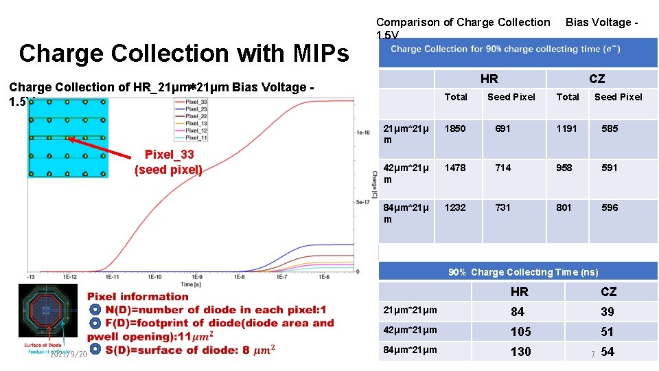
Charge Collection with MIPs Comparison of Charge Collection 1. 5 V HR Charge Collection of HR_21μm*21μm Bias Voltage 1. 5 V Pixel_33 (seed pixel) Bias Voltage - Total CZ Seed Pixel Total Seed Pixel 21μm*21μ m 1850 691 1191 585 42μm*21μ m 1478 714 958 591 84μm*21μ m 1232 731 801 596 90% Charge Collecting Time (ns) 2021/9/20 HR CZ 21μm*21μm 84 39 42μm*21μm 105 51 84μm*21μm 130 7 54

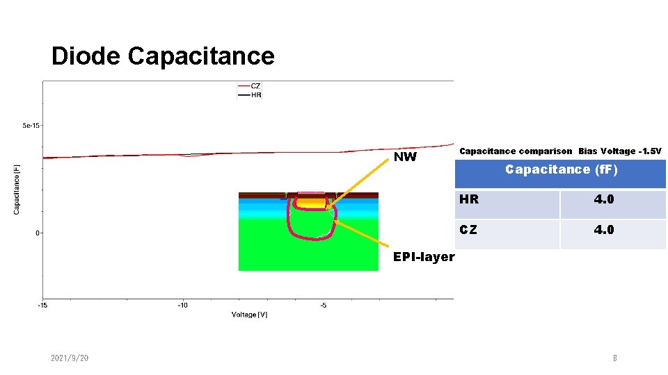
Diode Capacitance NW Capacitance comparison Bias Voltage -1. 5 V Capacitance (f. F) HR 4. 0 CZ 4. 0 EPI-layer 2021/9/20 8

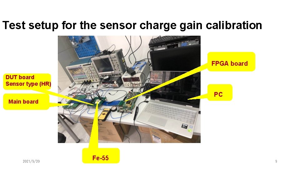
Test setup for the sensor charge gain calibration FPGA board DUT board Sensor type (HR) PC Main board 2021/9/20 Fe-55 9

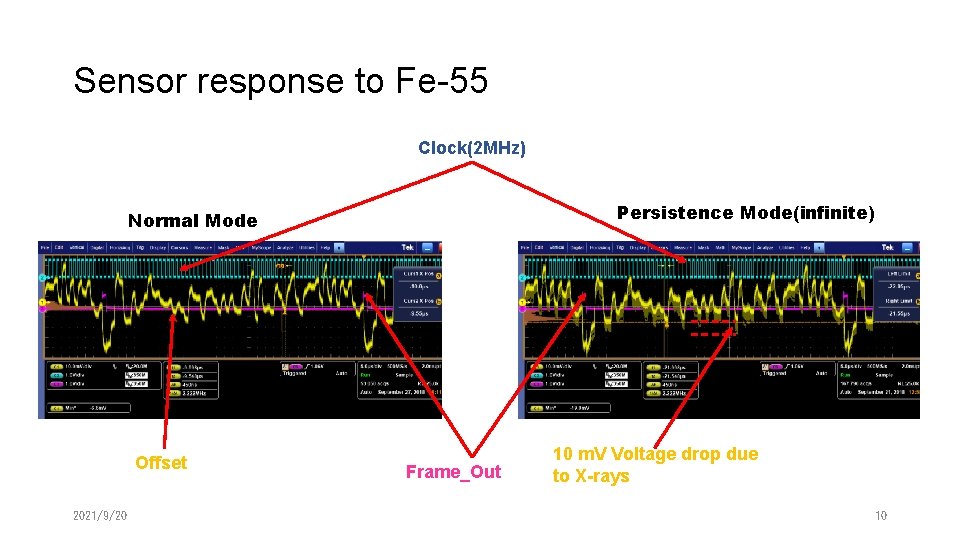
Sensor response to Fe-55 Clock(2 MHz) Persistence Mode(infinite) Normal Mode Offset 2021/9/20 Frame_Out 10 m. V Voltage drop due to X-rays 10

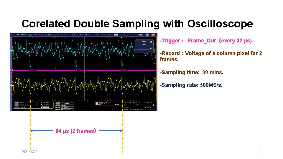
Corelated Double Sampling with Oscilloscope -Trigger: Frame_Out(every 32 μs). -Record:Voltage of a column pixel for 2 frames. -Sampling time: 30 mins. -Sampling rate: 500 MS/s. 64 μs (2 frames) 2021/9/20 11

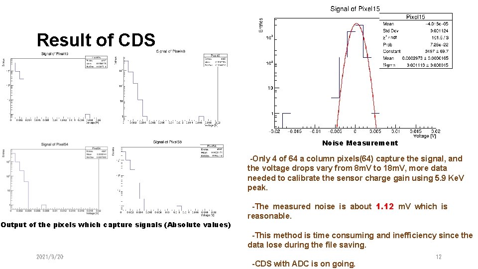
Result of CDS Noise Measurement -Only 4 of 64 a column pixels(64) capture the signal, and the voltage drops vary from 8 m. V to 18 m. V, more data needed to calibrate the sensor charge gain using 5. 9 Ke. V peak. Output of the pixels which capture signals (Absolute values) -The measured noise is about 1. 12 m. V which is reasonable. -This method is time consuming and inefficiency since the data lose during the file saving. 2021/9/20 -CDS with ADC is on going. 12

Summary ~2 types of sensors have been simulated , simulated values of Charge Collection and Diode Capacitance were given. ~Optimized geometry and sensor type were HR and 21μm*21μm,need test data to verify. ~CDS with ADC is on going. ~A telescope project has been applied by SDU Pixel group, and another 0. 18μm technology will be applied, these simulation and test result would be a guidance for next chip design. 2021/9/20 13