Systems Architecture Seventh Edition Chapter 6 System Integration
- Slides: 67

Systems Architecture, Seventh Edition Chapter 6 System Integration and Performance © 2016. Cengage Learning. All rights reserved.

Chapter Objectives • In this chapter, you will learn to: – Describe the system and subsidiary buses and bus protocol – Describe how the CPU and bus interact with peripheral devices – Describe the purpose and function of device controllers – Describe how interrupt processing coordinates the CPU with secondary storage and I/O devices © 2016. Cengage Learning. All rights reserved. Systems Architecture, Seventh Edition

Chapter Objectives (continued) • In this chapter, you will learn to: – Describe how buffers and caches improve computer system performance – Compare parallel processing architectures – Describe compression technology and its performance implications © 2016. Cengage Learning. All rights reserved. Systems Architecture, Seventh Edition

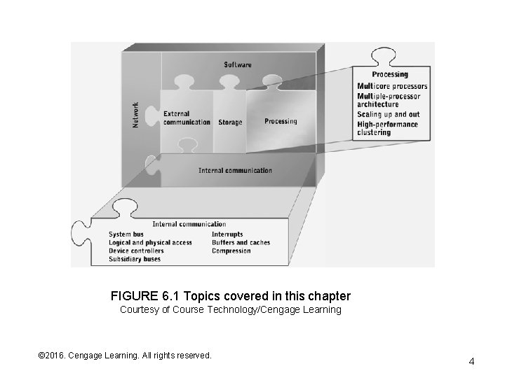
FIGURE 6. 1 Topics covered in this chapter Courtesy of Course Technology/Cengage Learning © 2016. Cengage Learning. All rights reserved. Systems Architecture, Seventh Edition 4

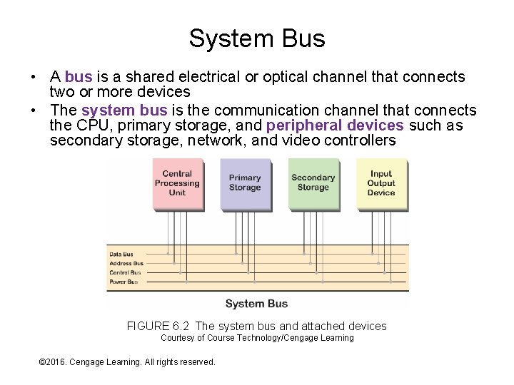
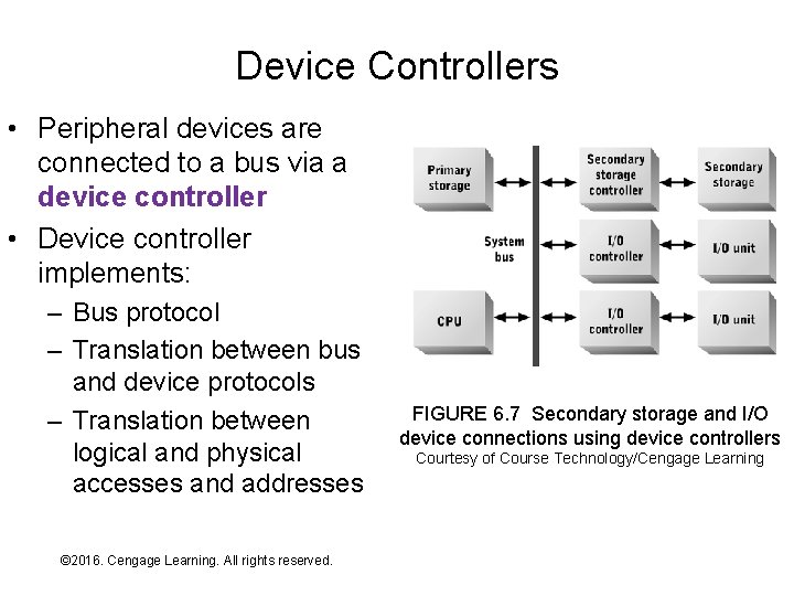
System Bus • A bus is a shared electrical or optical channel that connects two or more devices • The system bus is the communication channel that connects the CPU, primary storage, and peripheral devices such as secondary storage, network, and video controllers FIGURE 6. 2 The system bus and attached devices Courtesy of Course Technology/Cengage Learning © 2016. Cengage Learning. All rights reserved. Systems Architecture, Seventh Edition

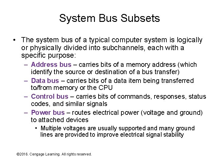
System Bus Subsets • The system bus of a typical computer system is logically or physically divided into subchannels, each with a specific purpose: – Address bus – carries bits of a memory address (which identify the source or destination of a bus transfer) – Data bus – carries bits of a data item being transferred to/from memory or the CPU – Control bus – carries bits of commands, responses, status codes, and similar signals – Power bus – routes electrical power (voltage and ground) to attached devices • Multiple voltages are usually supported and many ground lines are provided to improve electrical signal stability © 2016. Cengage Learning. All rights reserved. Systems Architecture, Seventh Edition

PCI Bus • Most desktop and laptop computers and many midrange computers implement some version of the Peripheral Component Interface (PCI) bus standard • Early PCI versions use parallel electrical connections (one per bit) – http: //www. interfacebus. com/Design_Connector_PCI_X. html – Address and data bus lines are shared (one sent immediately after the other in successive bus cycles – Parallel channels are relatively slow and require all attached devices to have the same physical interface and operate at the same clock speed • Later PCI versions incorporate serial data channels – http: //www. interfacebus. com/Design_PCI_Express_1 x_Pin. Out. html – Serial connectors are physically smaller due to fewer wires – Serial channels can operate at higher speed and can allow attached devices to operate a different fractions of the maximum speed • More on serial vs. parallel channels in Chapter 8 © 2016. Cengage Learning. All rights reserved. Systems Architecture, Seventh Edition

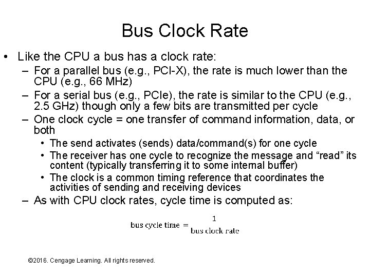
Bus Clock Rate • Like the CPU a bus has a clock rate: – For a parallel bus (e. g. , PCI-X), the rate is much lower than the CPU (e. g. , 66 MHz) – For a serial bus (e. g. , PCIe), the rate is similar to the CPU (e. g. , 2. 5 GHz) though only a few bits are transmitted per cycle – One clock cycle = one transfer of command information, data, or both • The send activates (sends) data/command(s) for one cycle • The receiver has one cycle to recognize the message and “read” its content (typically transferring it to some internal buffer) • The clock is a common timing reference that coordinates the activities of sending and receiving devices – As with CPU clock rates, cycle time is computed as: © 2016. Cengage Learning. All rights reserved. Systems Architecture, Seventh Edition

Bus Clock Rate - Continued • The system bus must be relatively long because it connects all devices in the system – Long length = long distance for electricity to travel – Electricity speed is constant – Thus, clock rate goes up as length goes down (assuming all other things are equal) • Length determines a theoretical maximum clock rate, but the actual rate is usually far less because: – – Probability of error increases with speed Faster/error-free devices are more expensive Bus is a chain, only as fast as its slowest device Cost/performance trade-off © 2016. Cengage Learning. All rights reserved. Systems Architecture, Seventh Edition

Bus Data Transfer Rate • The data transfer rate of a bus is computed as: Bus DTR = data transfer unit size × clock rate – For older an older parallel bus, slow clock rate is partly mitigated by a relatively large data transfer unit size, for example: Bus DTR = 64 bits × 66 MHz = 8 bytes × 66, 000 = 528, 000 bytes per second = 528 MBps – For a newer serial bus, higher clock rates look good but data transfer unit size is low Bus DTR = 1 bit × 2. 5 GHz = 1 bit × 2, 500, 000 = 2, 500, 000 bits per second = 312. 5 MBps • Data transfer rate can only be increased by: – Increasing clock rate – Increasing number of bits transmitted per clock cycle (data transfer unit size) – Using a more efficient bus protocol © 2016. Cengage Learning. All rights reserved. Systems Architecture, Seventh Edition

Bus Protocol • The bus protocol is the “language” of the bus: – – Which lines are used for what purposes? What are the electrical or optical characteristics of each signal? How are bit values encoded in a line? How are commands, errors, and status information encoded in bit values on the control bus? – Which device(s) get to use the bus when? How do they “ask” for access? For how long do they have access? • Bus protocols vary in their efficiency, for example – Consider a bus in which a command is transferred in one cycle and the data is transferred in the next – Effective data transfer rate is half that computed previously because only half the cycles carry “real” data • Efficient protocols tend to be more complex: – Require a more complex command structure and thus more control bus lines – Require more lines to carry data, address, and command information all at the same time – Bus and all devices that interface with it are more expensive © 2016. Cengage Learning. All rights reserved. Systems Architecture, Seventh Edition

Bus Masters • Two approaches to controlling bus access: – Master-slave bus • Bus master (CPU or a designated device) controls all bus transfers • All other devices are bus slaves • Simple but relatively inefficient because the bus master is a bottleneck – Peer-to-peer bus • Any device can temporarily become a bus master • Requires a protocol for “passing around” the bus master role and a prioritization scheme for competing requests to be bus master © 2016. Cengage Learning. All rights reserved. Systems Architecture, Seventh Edition

Bus Memory Access • The data transfer rate mismatch between the system bus and the CPU is usually two orders of magnitude or more: – Direct interface would waste many CPU cycles • To improve performance: – Data transfers to/from the CPU go “through” memory – commonly called direct memory access (DMA) – CPU becomes a bus master only when absolutely necessary © 2016. Cengage Learning. All rights reserved. Systems Architecture, Seventh Edition

Multiple Buses • In the “bad old days” there was only the system bus and all devices were connected to it – Computer system, bus, and connected devices were relatively simple – Inefficiencies resulted because system-wide performance was limited by the slowest devices • In the modern world there are multiple buses for different purposes, each optimized for a particular purpose or kind of data communication – The system bus still connects many of the devices in the system (e. g. , network, USB, keyboard, …) – Separate bus connects CPU to memory (e. g. , Intel’s Front-Side Bus) • High clock rate (shorter distance) • Supports two-way communication – Separate bus for video (AGP video card slot on PCs, ± 2005 -2010) • Connects memory to video controller • High clock rate (shorter distance) • Data transfer is one-way – Other separate buses • Secondary storage (e. g. , SCSI and SATA) • External devices (USB and Firewire) © 2016. Cengage Learning. All rights reserved. Systems Architecture, Seventh Edition

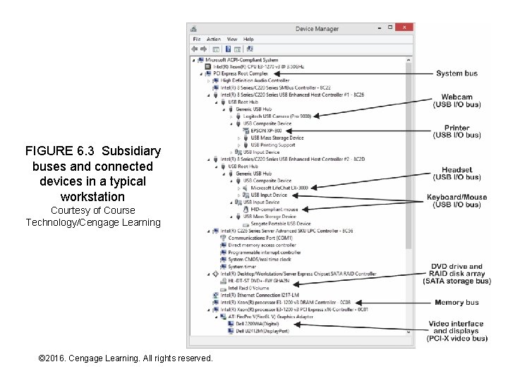
Exercise • On a Windows machine: – – Right-click on My Computer and Select Properties Select Device Manager On the View menu select Devices by connection Click + symbols in the display to examine connections among devices: • Start with nodes that have ACPI in their names • Look for specific buses such as “PCI bus” • Use the device manager to sketch a “map” of device and bus interconnections (see Figure 6. 3 for an example) © 2016. Cengage Learning. All rights reserved. Systems Architecture, Seventh Edition

FIGURE 6. 3 Subsidiary buses and connected devices in a typical workstation Courtesy of Course Technology/Cengage Learning © 2016. Cengage Learning. All rights reserved. Systems Architecture, Seventh Edition

Device Access • An input/output (I/O) port is: – A communication pathway between the CPU and a peripheral device – A set of memory addresses through which data is passed between the CPU and one peripheral device – A logical abstraction that enables the CPU to interact with all devices using the same protocol • CPU interface to bus devices is simpler, thus more efficient and faster • New devices can be incorporated into an existing computer – Install device into available bus slot – Assign one or more I/O ports – Add an appropriate device driver to the operating system © 2016. Cengage Learning. All rights reserved. Systems Architecture, Seventh Edition

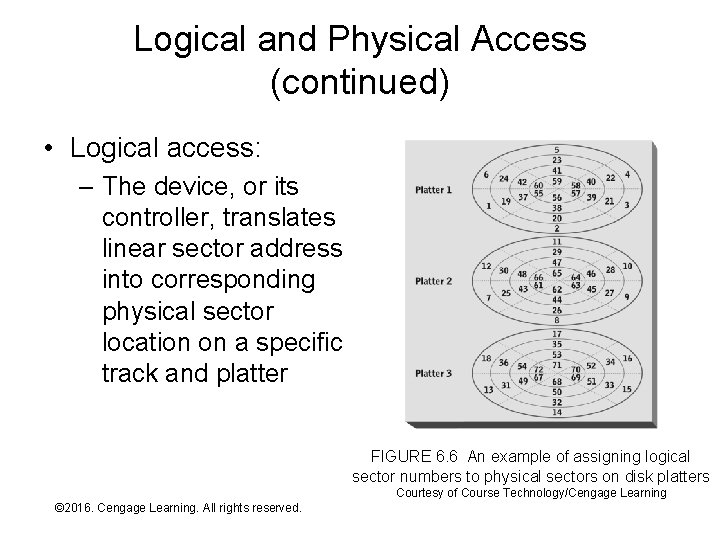
Logical and Physical Device Accesses • The CPU interacts with each device as though it were a storage device with sequentially organized storage locations (e. g. , a magnetic tape) – The storage locations of the hypothetical device is a linear address space – a sequence of storage locations number starting with zero – A read (device to CPU) or write (CPU to device) operation is called a logical access – The device or a device controller translates logical accesses into physical accesses – The translation specifics vary depending on the device specifics © 2016. Cengage Learning. All rights reserved. Systems Architecture, Seventh Edition

Logical and Physical Accesses Continued • Sample logical/physical translations: – Keyboard – no write operations, read transfers a few bytes representing the last keystroke – Video • Assign addresses to pixel locations (e. g. , top row is 01919, next row is 1920 -3839, …) • Pixel update sends address followed by a few bytes describing the pixel content – Disk • Assign addresses to sectors, typically by sector within track, then recording surface within cylinder starting at the outer edge of the platters • Read/write sends sector address then 5412 bytes of data © 2016. Cengage Learning. All rights reserved. Systems Architecture, Seventh Edition

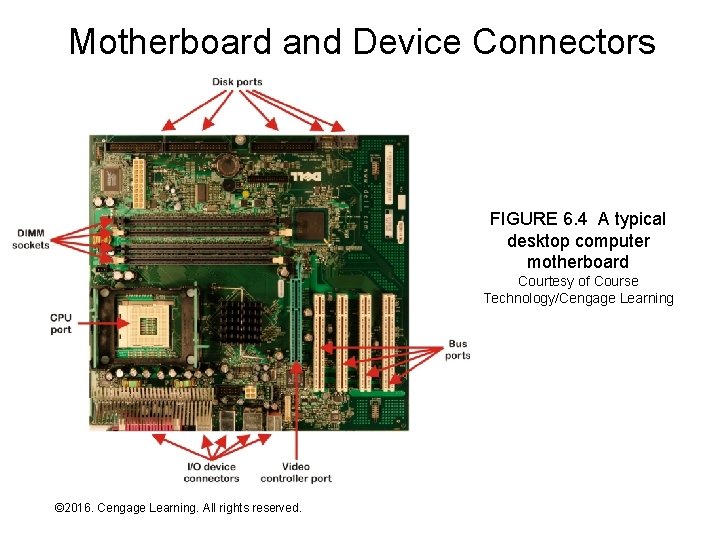
Motherboard and Device Connectors FIGURE 6. 4 A typical desktop computer motherboard Courtesy of Course Technology/Cengage Learning © 2016. Cengage Learning. All rights reserved. Systems Architecture, Seventh Edition

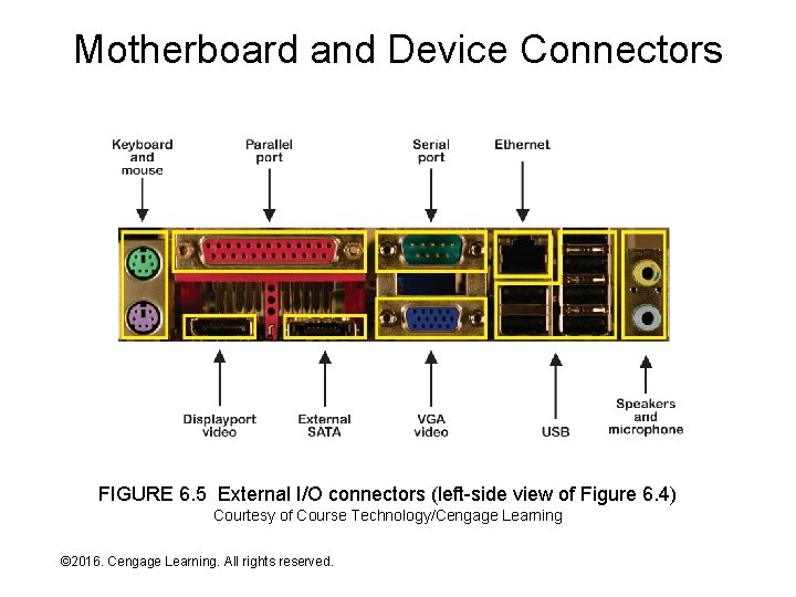
Motherboard and Device Connectors FIGURE 6. 5 External I/O connectors (left-side view of Figure 6. 4) Courtesy of Course Technology/Cengage Learning © 2016. Cengage Learning. All rights reserved. Systems Architecture, Seventh Edition

Logical and Physical Access (continued) • Logical access: – The device, or its controller, translates linear sector address into corresponding physical sector location on a specific track and platter FIGURE 6. 6 An example of assigning logical sector numbers to physical sectors on disk platters Courtesy of Course Technology/Cengage Learning © 2016. Cengage Learning. All rights reserved. Systems Architecture, Seventh Edition

Device Controllers • Peripheral devices are connected to a bus via a device controller • Device controller implements: – Bus protocol – Translation between bus and device protocols – Translation between logical and physical accesses and addresses © 2016. Cengage Learning. All rights reserved. Systems Architecture, Seventh Edition FIGURE 6. 7 Secondary storage and I/O device connections using device controllers Courtesy of Course Technology/Cengage Learning

Device Controllers - Continued • A device controller can connect multiple devices to a single bus slot – Reduces number of bus slots and bus length – Enables higher bus clock rates – Combines the smaller I/O capacity of multiple devices to match the larger capacity of the bus • An I/O channel is a device controller “on steroids” – Typically found only in mainframes – Implemented as a special purpose computer – Connects dozens of physical devices to a single bus port – Can support a variety of different device types © 2016. Cengage Learning. All rights reserved. Systems Architecture, Seventh Edition

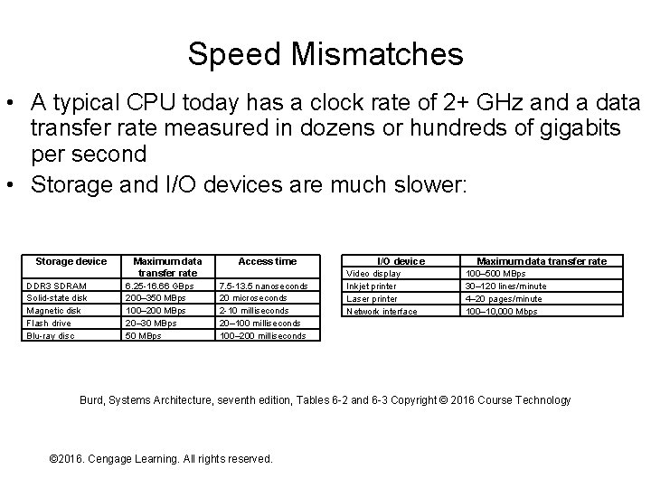
Speed Mismatches • A typical CPU today has a clock rate of 2+ GHz and a data transfer rate measured in dozens or hundreds of gigabits per second • Storage and I/O devices are much slower: Storage device DDR 3 SDRAM Solid-state disk Magnetic disk Flash drive Blu-ray disc Maximum data transfer rate 6. 25 -16. 66 GBps 200– 350 MBps 100– 200 MBps 20– 30 MBps 50 MBps Access time 7. 5 -13. 5 nanoseconds 20 microseconds 2 -10 milliseconds 20– 100 milliseconds 100– 200 milliseconds I/O device Video display Inkjet printer Laser printer Network interface Maximum data transfer rate 100– 500 MBps 30– 120 lines/minute 4– 20 pages/minute 100– 10, 000 Mbps Burd, Systems Architecture, seventh edition, Tables 6 -2 and 6 -3 Copyright © 2016 Course Technology © 2016. Cengage Learning. All rights reserved. Systems Architecture, Seventh Edition

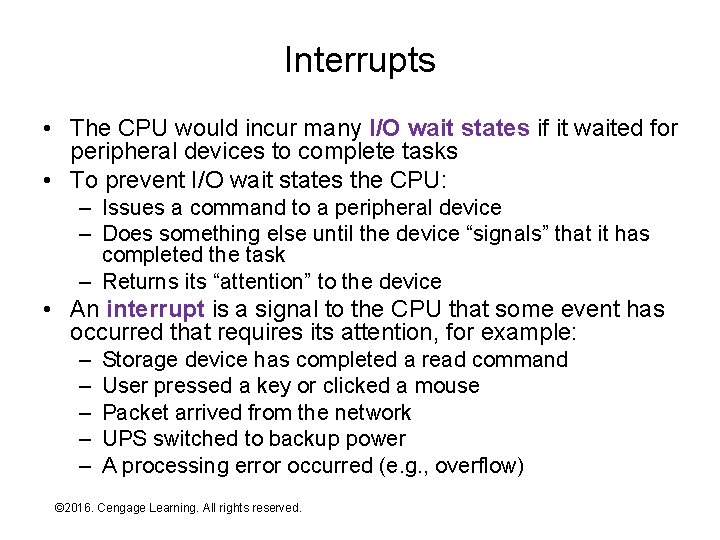
Interrupts • The CPU would incur many I/O wait states if it waited for peripheral devices to complete tasks • To prevent I/O wait states the CPU: – Issues a command to a peripheral device – Does something else until the device “signals” that it has completed the task – Returns its “attention” to the device • An interrupt is a signal to the CPU that some event has occurred that requires its attention, for example: – – – Storage device has completed a read command User pressed a key or clicked a mouse Packet arrived from the network UPS switched to backup power A processing error occurred (e. g. , overflow) © 2016. Cengage Learning. All rights reserved. Systems Architecture, Seventh Edition

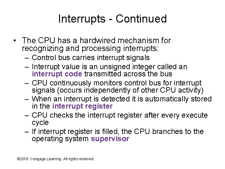
Interrupts - Continued • The CPU has a hardwired mechanism for recognizing and processing interrupts: – Control bus carries interrupt signals – Interrupt value is an unsigned integer called an interrupt code transmitted across the bus – CPU continuously monitors control bus for interrupt signals (occurs independently of other CPU activity) – When an interrupt is detected it is automatically stored in the interrupt register – CPU checks the interrupt register after every execute cycle – If interrupt register is filled, the CPU branches to the operating system supervisor © 2016. Cengage Learning. All rights reserved. Systems Architecture, Seventh Edition

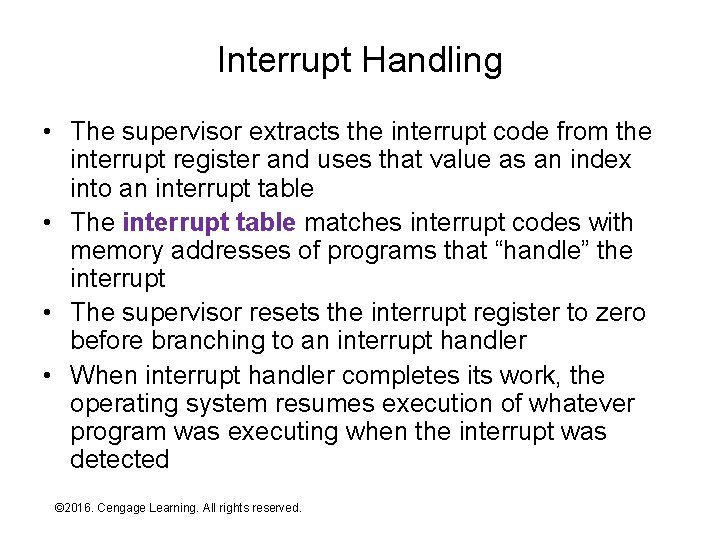
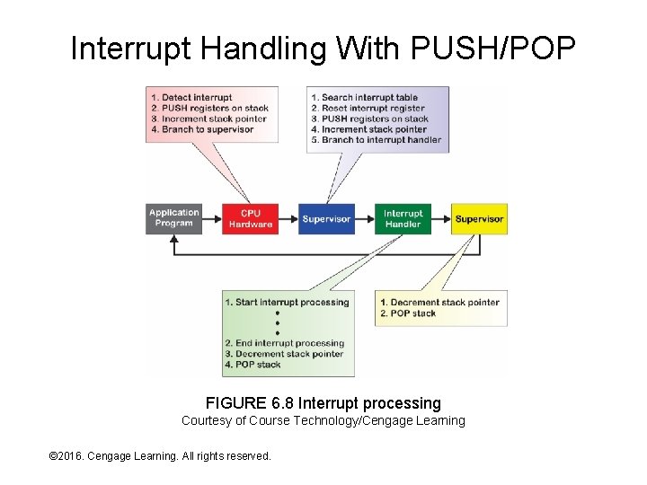
Interrupt Handling • The supervisor extracts the interrupt code from the interrupt register and uses that value as an index into an interrupt table • The interrupt table matches interrupt codes with memory addresses of programs that “handle” the interrupt • The supervisor resets the interrupt register to zero before branching to an interrupt handler • When interrupt handler completes its work, the operating system resumes execution of whatever program was executing when the interrupt was detected © 2016. Cengage Learning. All rights reserved. Systems Architecture, Seventh Edition

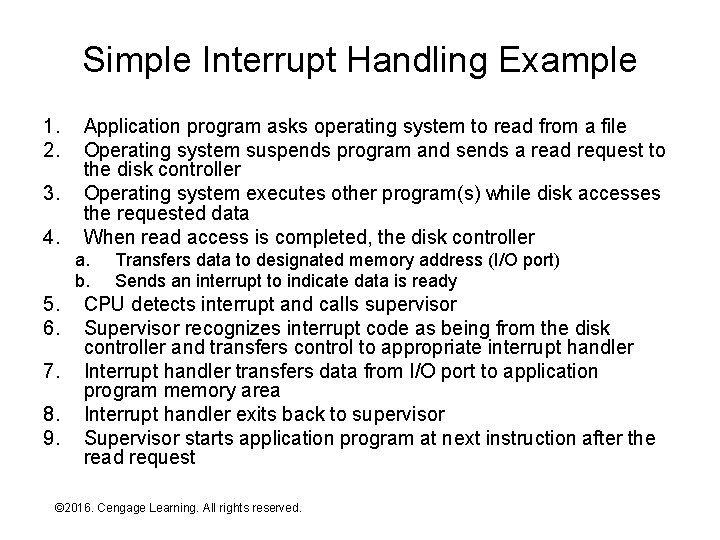
Simple Interrupt Handling Example 1. 2. 3. 4. Application program asks operating system to read from a file Operating system suspends program and sends a read request to the disk controller Operating system executes other program(s) while disk accesses the requested data When read access is completed, the disk controller a. b. 5. 6. 7. 8. 9. Transfers data to designated memory address (I/O port) Sends an interrupt to indicate data is ready CPU detects interrupt and calls supervisor Supervisor recognizes interrupt code as being from the disk controller and transfers control to appropriate interrupt handler Interrupt handler transfers data from I/O port to application program memory area Interrupt handler exits back to supervisor Supervisor starts application program at next instruction after the read request © 2016. Cengage Learning. All rights reserved. Systems Architecture, Seventh Edition

Exercise • Assume that you are viewing a web page and click on a hyperlink to bring up another page • Describe the interrupt processing sequence that coordinates access to the new page across the network (ignore the mouse click itself) © 2016. Cengage Learning. All rights reserved. Systems Architecture, Seventh Edition

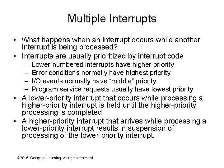
Multiple Interrupts • What happens when an interrupt occurs while another interrupt is being processed? • Interrupts are usually prioritized by interrupt code – – Lower-numbered interrupts have higher priority Error conditions normally have highest priority I/O events normally have “middle” priority Program service requests usually have lowest priority • A lower-priority interrupt that occurs while processing a higher-priority interrupt is held until the higher-priority processing is completed • A higher-priority interrupt that arrives while processing a lower-priority interrupt results in suspension of processing of the lower-priority interrupt. © 2016. Cengage Learning. All rights reserved. Systems Architecture, Seventh Edition

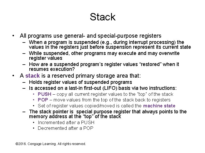
Stack • All programs use general- and special-purpose registers – When a program is suspended (e. g. , during interrupt processing) the values in the registers just before suspension represent its current state – While suspended, other programs may execute and may overwrite register values – How are a suspended program’s register values “restored” when it resumes execution? • A stack is a reserved primary storage area that: – Holds register values of suspended programs – Is accessed on a last-in first-out (LIFO) basis via two instructions: • PUSH – copy all current register values to the “top” of the stack • POP – move values from the top of the stack back to registers • Set of register values copied/moved is called the machine state – The stack pointer is special purpose register that always points to the memory address at the “top” of the stack • Incremented after a PUSH • Decremented after a POP © 2016. Cengage Learning. All rights reserved. Systems Architecture, Seventh Edition

Interrupt Handling With PUSH/POP FIGURE 6. 8 Interrupt processing Courtesy of Course Technology/Cengage Learning © 2016. Cengage Learning. All rights reserved. Systems Architecture, Seventh Edition

Buffering and Caching • Buffering and caching are both techniques that use “extra” primary storage to improve performance – Buffer – a small storage area that holds data in transit from one device or location to another – Cache – a “fast” storage area used to improve the performance of read/write accesses to a slower storage device • Though both use RAM, they use it in different amounts and different ways to achieve performance improvements © 2016. Cengage Learning. All rights reserved. Systems Architecture, Seventh Edition

Buffers • The source and destination of an I/O operation typically different in two important respects: – Speed of data transfer – Data transfer unit size • A buffer can improve the efficiency of the faster device during an I/O operation by: – Reducing the number of interruptions – Reducing processing overhead for the interruptions • A buffer is generally required when data unit transfer sizes differ • Data flows through a buffer: – The sending device adds data to the buffer, gradually filling it – The receiving device (or buffer manager) consumes data in the buffer, gradually emptying it – The content of the buffer rises and falls depending on the timing and relative speed of addition and consumption © 2016. Cengage Learning. All rights reserved. Systems Architecture, Seventh Edition

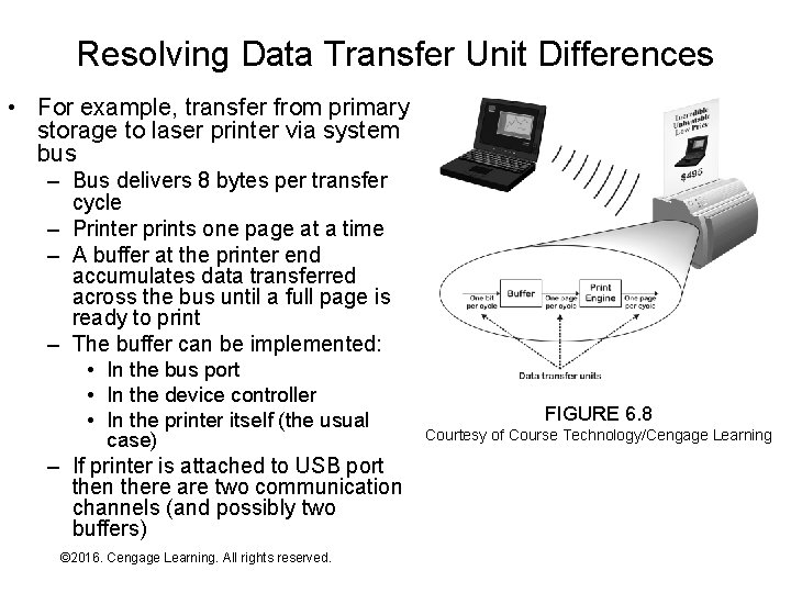
Resolving Data Transfer Unit Differences • For example, transfer from primary storage to laser printer via system bus – Bus delivers 8 bytes per transfer cycle – Printer prints one page at a time – A buffer at the printer end accumulates data transferred across the bus until a full page is ready to print – The buffer can be implemented: • In the bus port • In the device controller • In the printer itself (the usual case) – If printer is attached to USB port then there are two communication channels (and possibly two buffers) © 2016. Cengage Learning. All rights reserved. Systems Architecture, Seventh Edition FIGURE 6. 8 Courtesy of Course Technology/Cengage Learning

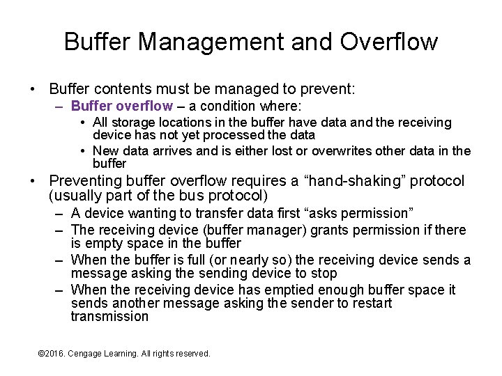
Buffer Management and Overflow • Buffer contents must be managed to prevent: – Buffer overflow – a condition where: • All storage locations in the buffer have data and the receiving device has not yet processed the data • New data arrives and is either lost or overwrites other data in the buffer • Preventing buffer overflow requires a “hand-shaking” protocol (usually part of the bus protocol) – A device wanting to transfer data first “asks permission” – The receiving device (buffer manager) grants permission if there is empty space in the buffer – When the buffer is full (or nearly so) the receiving device sends a message asking the sending device to stop – When the receiving device has emptied enough buffer space it sends another message asking the sender to restart transmission © 2016. Cengage Learning. All rights reserved. Systems Architecture, Seventh Edition

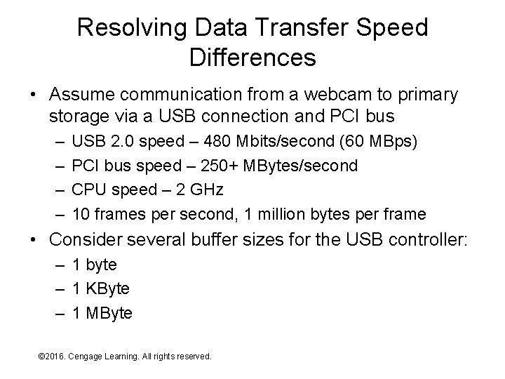
Resolving Data Transfer Speed Differences • Assume communication from a webcam to primary storage via a USB connection and PCI bus – – USB 2. 0 speed – 480 Mbits/second (60 MBps) PCI bus speed – 250+ MBytes/second CPU speed – 2 GHz 10 frames per second, 1 million bytes per frame • Consider several buffer sizes for the USB controller: – 1 byte – 1 KByte – 1 MByte © 2016. Cengage Learning. All rights reserved. Systems Architecture, Seventh Edition

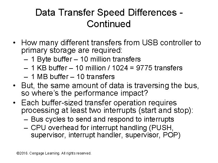
Data Transfer Speed Differences Continued • How many different transfers from USB controller to primary storage are required: – 1 Byte buffer – 10 million transfers – 1 KB buffer – 10 million / 1024 = 9775 transfers – 1 MB buffer – 10 transfers • But, the same amount of data is traversing the bus, so where’s the performance impact? • Each buffer-sized transfer operation requires processing at least two interrupts (start and stop): – Bus cycles to send and respond to interrupts – CPU overhead for interrupt handling (PUSH, supervisor, interrupt handler, supervisor, POP) © 2016. Cengage Learning. All rights reserved. Systems Architecture, Seventh Edition

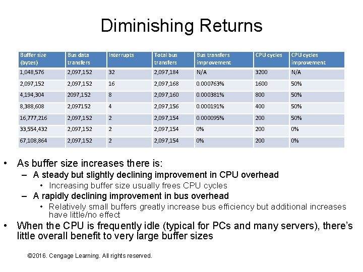
Diminishing Returns Buffer size (bytes) Bus data transfers Interrupts Total bus transfers Bus transfers improvement CPU cycles improvement 1, 048, 576 2, 097, 152 32 2, 097, 184 N/A 3200 N/A 2, 097, 152 16 2, 097, 168 0. 000763% 1600 50% 4, 194, 304 2097, 152 8 2, 097, 160 0. 000381% 800 50% 8, 388, 608 2, 097152 4 2, 097, 156 0. 000191% 400 50% 16, 777, 216 2, 097, 152 2 2, 097, 154 0. 000095% 200 50% 33, 554, 432 2, 097, 152 2 2, 097, 154 0% 200 0% 67, 108, 864 2, 097, 152 2 2, 097, 154 0% 200 0% • As buffer size increases there is: – A steady but slightly declining improvement in CPU overhead • Increasing buffer size usually frees CPU cycles – A rapidly declining improvement in bus overhead • Relatively small buffers greatly increase bus efficiency but additional increases have little/no effect • When the CPU is frequently idle (typical for PCs and many servers), there’s little overall benefit to very large buffer sizes © 2016. Cengage Learning. All rights reserved. Systems Architecture, Seventh Edition

Cache v Cache – a “fast” storage area used to improve the performance of read/write accesses to a slower storage device • How does a cache differ from a buffer? – – – Reading from a cache doesn’t consume the data Cache is used for bidirectional data transfer Cache is used only for storage devices A cache is usually much larger than a buffer More “intelligence” is require to manage cache content • Cache-related performance improvements depend on: – Cache size – Cache management intelligence © 2016. Cengage Learning. All rights reserved. Systems Architecture, Seventh Edition

Quick Exercise • Caching is commonly used today within microprocessors and secondary storage controllers • Cache sizes and management sophistication have grown over time – for example, – Hard disks typically have 8 -32 MB of embedded cache (none 20 years ago) – Microprocessors typically have three levels of primary storage cache with the largest measured in dozens of megabytes (one level measured in kilobytes 20 years ago) • Why is caching so much more prevalent today than it was twenty years ago? • Hint: Last 10 pages of Chapter 4 © 2016. Cengage Learning. All rights reserved. Systems Architecture, Seventh Edition

Caching and Performance • Cache performance principles: – If the cache is faster than the underlying storage device then access to the cache (read or write) will be faster than access to the underlying storage device – For reading, can we guess what will be read next from the storage device and put it in the cache “ahead of time”? – For writing, can we (quickly) place the data in the cache and copy it to the storage device later? © 2016. Cengage Learning. All rights reserved. Systems Architecture, Seventh Edition

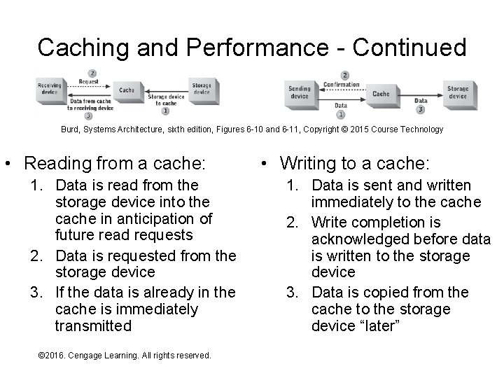
Caching and Performance - Continued Burd, Systems Architecture, sixth edition, Figures 6 -10 and 6 -11, Copyright © 2015 Course Technology • Reading from a cache: 1. Data is read from the storage device into the cache in anticipation of future read requests 2. Data is requested from the storage device 3. If the data is already in the cache is immediately transmitted © 2016. Cengage Learning. All rights reserved. Systems Architecture, Seventh Edition • Writing to a cache: 1. Data is sent and written immediately to the cache 2. Write completion is acknowledged before data is written to the storage device 3. Data is copied from the cache to the storage device “later”

Delayed Write Risk • Immediate acknowledgement of a write operation has risks: – Cache is implemented with RAM and is thus volatile – If power is lost or the system crashes after write acknowledgement but before the write to the storage device completes then the written data is “lost” • Immediate write acknowledge can be: – Enabled – maximizes performance improvement associated with write caching – Selectively enabled – difficult/complex to implement – Disabled – minimizes or eliminates performance improvement associated with write caching (effectively turns the write cache into a large buffer) © 2016. Cengage Learning. All rights reserved. Systems Architecture, Seventh Edition

Cache Controller • Most of the performance gain associated with caching comes from read operations: – Read after write (small gain) – Read-ahead (large gain) • A cache controller is a processor that manages cache content – Often a dedicated processor, for example: • Circuitry that manages an L 2 on-chip cache in a Core 2 • A low-end CPU plus ROM in a secondary storage controller – Can be a program run “part-time” in a generalpurpose CPU if the cache is implemented with primary storage © 2016. Cengage Learning. All rights reserved. Systems Architecture, Seventh Edition

Cache Controller - Continued • The most important impact of a cache controller on performance is its accuracy in guessing what data is most likely to be needed next: – Cache hit – Read access for data already in the cache – Cache miss – Read access for data not already in the cache – Cache swap – Replacement of existing data in cache with data from the storage device – Hit ratio – cache hits as a % of read operations • Ideal cache controller has 100% hit ratio • Cache is usually cost-effective if hit ratio > 60% • Hit ratio depends on nature of read operations (e. g. , random vs. sequential reads) © 2016. Cengage Learning. All rights reserved. Systems Architecture, Seventh Edition

Cache Size • Surprising small cache sizes (relative to storage device size) can yield significant improvements • Typical ratios of storage device size to cache size range from 1, 000: 1 to 10, 000: 1, for example: – Typical PC primary storage cache • On-chip CPU cache: 2 MBytes • Installed RAM: 4 GBytes • Size ratio 2048: 1 – Typical server secondary storage cache • RAM dedicated to secondary storage cache: 4 GBytes • Secondary storage capacity: 20 Terabytes • Size ratio 5000: 1 © 2016. Cengage Learning. All rights reserved. Systems Architecture, Seventh Edition

Primary Storage Caching • Terminology (assuming 3 cache levels exist): – L 1 cache – integrated with each CPU’s control unit – L 2 cache – implemented outside of but dedicated to a single CPU – L 3 cache – shared among multiple CPU cores ona single chip • There’s lots of “extra space” on modern chips to implement very large SRAM L 2 and L 3 caches © 2016. Cengage Learning. All rights reserved. Systems Architecture, Seventh Edition

Secondary Storage Caching • Through the 1990 s secondary storage caches were typically implemented on the secondary storage controller with: – A special purpose processor as the cache controller – Installed memory chips or DIMMs • Since that time, secondary storage cache is usually implemented using: – “Extra” system RAM – Cache management by the OS using the CPU • Why the change? – Most computer systems have “extra CPU cycles” – System RAM is cheap and motherboards have been redesigned to accommodate lots of it – The operating system can best decide how to allocate RAM for performance improvement – secondary storage cache or other purposes – not possible if RAM is on device controller – The operating system is in the best position to make cache replacement decisions since it processes all secondary storage operations (via service layer calls) and thus “knows” their pattern(s) © 2016. Cengage Learning. All rights reserved. Systems Architecture, Seventh Edition

Processing Parallelism • Many applications are too big for most/any single computer, for example: – Large-scale transaction processing – Data mining – Large-scale numerical simulations • Parallel processing: – Breaks large problems up into smaller pieces – Allocates problem pieces to multiple compute nodes – Reassembles piece-wise solutions • Common parallel processing architectures include: – Multicore microprocessors – Multi-CPU architectures – Multicomputer architectures (clusters and grids) © 2016. Cengage Learning. All rights reserved. Systems Architecture, Seventh Edition

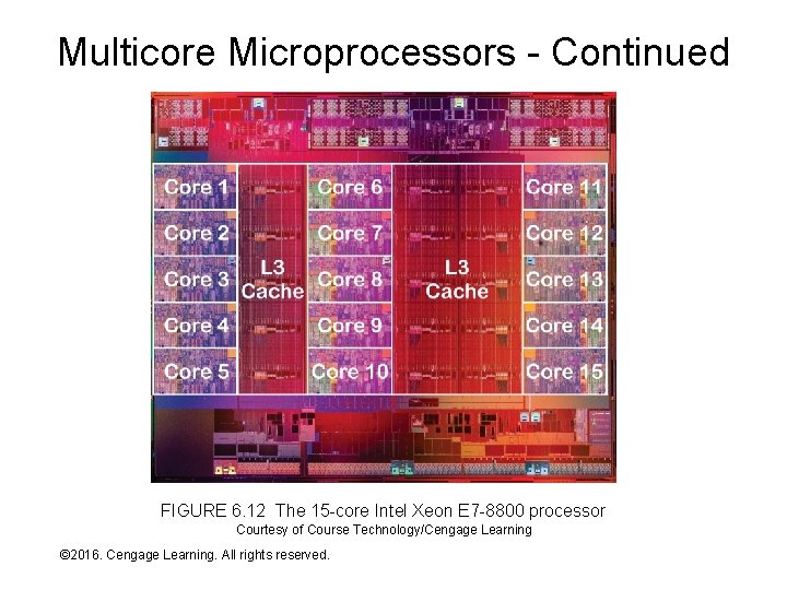
Multicore Microprocessors • A multicore microprocessor places: – Multiple processing cores (roughly comparable to a CPU) on a single chip – Usually includes one or more large (multi-megabyte) L 3 primary storage caches • Multicore chips are a natural consequence of two current semiconductor fabrication realities: – Increasing difficulty shrinking process size and increasing clock rate – Better luck at increasing transistor count • The latest chips are 8 -way, 12 -way, and 15 -way, but higher core counts are expected through the next decade • I/O data transfer capacity struggles to keep pace! © 2016. Cengage Learning. All rights reserved. Systems Architecture, Seventh Edition

Multicore Microprocessors - Continued FIGURE 6. 12 The 15 -core Intel Xeon E 7 -8800 processor Courtesy of Course Technology/Cengage Learning © 2016. Cengage Learning. All rights reserved. Systems Architecture, Seventh Edition

Multi-CPU Architecture • Multi-CPU architecture employs multiple microprocessors on a single motherboard sharing: – – Primary storage Secondary storage System bus I/O devices • Today, each “CPU” is usually a multicore microprocessor • This architecture is common in midrange and mainframe computers • It’s less common today in workstations as microprocessor core counts increase © 2016. Cengage Learning. All rights reserved. Systems Architecture, Seventh Edition

Scaling Up vs. Scaling Out • Scaling up – increasing available computer power by employing powerful computers, for example – Multicore microprocessors – Multi-CPU architecture • Scaling out – increasing available computer power by employing multiple computers in parallel, for example: – Clusters – Grids • Scaling out is gradually (but not completely) supplanting scaling up: – The gap between network vs. “within computer” data transfer rates has narrowed, though it’s still several orders of magnitude – Software for managing multicomputer configurations has improved significantly – morphing into “cloud” computing – Organizational need for flexibility – need to be able to quickly redeploy computing resources © 2016. Cengage Learning. All rights reserved. Systems Architecture, Seventh Edition

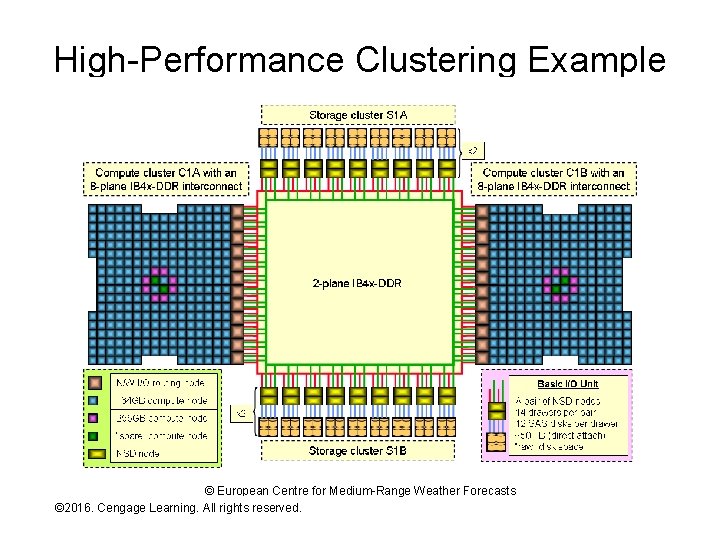
High-Performance Clustering Example © European Centre for Medium-Range Weather Forecasts © 2016. Cengage Learning. All rights reserved. Systems Architecture, Seventh Edition

High-Performance Clustering Example Continued • Each node is a 32 -CPU rack • Groups of 16 racks are directly connected • Each rack group is interconnected by a high-speed 8 -way switch • Specialized rack groups manage all secondary storage access • Architecture is optimized for: – Parallel processing with significant need for inter-node communication – Flexible assignment of compute nodes to problems and problem pieces © 2016. Cengage Learning. All rights reserved. Systems Architecture, Seventh Edition

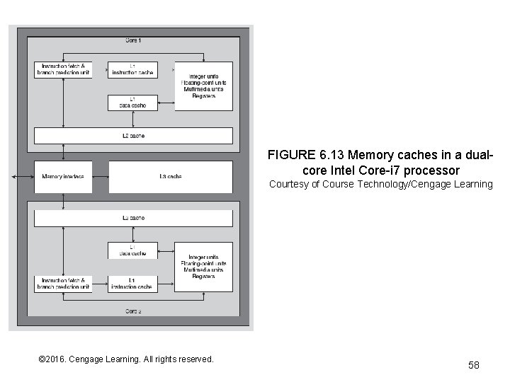
FIGURE 6. 13 Memory caches in a dualcore Intel Core-i 7 processor Courtesy of Course Technology/Cengage Learning © 2016. Cengage Learning. All rights reserved. Systems Architecture, Seventh Edition 58

Compression • Compression - a technique that reduces the number of bits used to encode a set of data items (e. g. , a file or a stream of motion video images): – Compression algorithm – computational technique for reducing data size – Decompression algorithm – computational technique for reversing compression algorithm – Compression ratio – Ratio of uncompressed to compressed data size (often an average) © 2016. Cengage Learning. All rights reserved. Systems Architecture, Seventh Edition

Lossy and Lossless Compression • Lossless compression – Compression followed by decompression exactly reproduces original data – Generally used for data such as files containing programs or numeric data (e. g. , ZIP files) • Lossy compression – Compressing then decompressing does not reproduce original data (common with audio and still/motion video) • Two common approaches to lossy compression: – Decompression algorithm isn’t a mirror of the compression algorithm (e. g. , PDF) – There is no decompression algorithm (e. g. , MP 3) or the decompression algorithm is really just a decoding algorithm (e. g. , video DVD) • With lossy compression, quality generally decreases as compression ratio increases, all other things being equal – For example, 64 Kbit/sec MP 3 files sound worse than 256 Kbit/sec MP 3 files – Quality loss can be somewhat offset by extra processing resources but only if a decompression algorithm is in use © 2016. Cengage Learning. All rights reserved. Systems Architecture, Seventh Edition

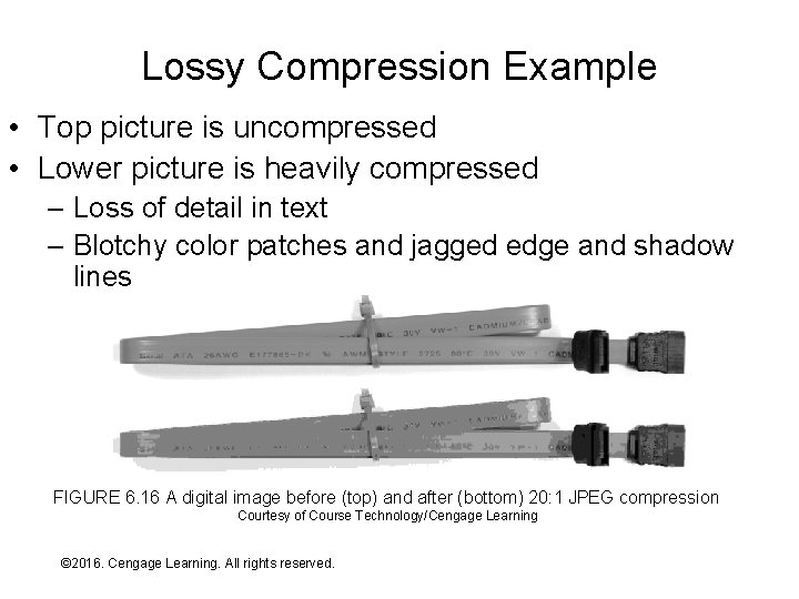
Lossy Compression Example • Top picture is uncompressed • Lower picture is heavily compressed – Loss of detail in text – Blotchy color patches and jagged edge and shadow lines FIGURE 6. 16 A digital image before (top) and after (bottom) 20: 1 JPEG compression Courtesy of Course Technology/Cengage Learning © 2016. Cengage Learning. All rights reserved. Systems Architecture, Seventh Edition

Compression - Continued • Compression and decompression algorithms consume processing resources (CPU and primary storage) while reducing data size: – Using compression substitutes processing resources for data communication or storage resources – A “classic” economic substitution scenario • Compression makes economic sense in either of the following situations: – Uncompressed data exceeds current technology capabilities at any reasonable cost (e. g. , HD-DVD) – Processing resources consumed by compression and decompression are less expensive than the saved storage or data communication resources (e. g. , H. 323 videoconferencing) © 2016. Cengage Learning. All rights reserved. Systems Architecture, Seventh Edition

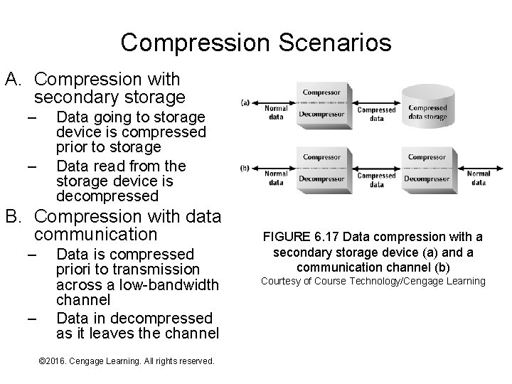
Compression Scenarios A. Compression with secondary storage – – Data going to storage device is compressed prior to storage Data read from the storage device is decompressed B. Compression with data communication – – Data is compressed priori to transmission across a low-bandwidth channel Data in decompressed as it leaves the channel © 2016. Cengage Learning. All rights reserved. Systems Architecture, Seventh Edition FIGURE 6. 17 Data compression with a secondary storage device (a) and a communication channel (b) Courtesy of Course Technology/Cengage Learning

Compression - Continued • Rapid increases in processor performance relative to data communication and storage performance has made compression increasingly attractive: – MP 3 and similar audio compression techniques – GIF and JPEG – Video DVDs – H. 323 video-conferencing – Compressed tape formats – Automatic compression of “old” files on secondary storage © 2016. Cengage Learning. All rights reserved. Systems Architecture, Seventh Edition

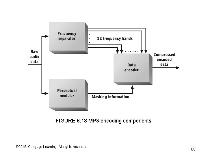
MPEG and MP 3 • Moving Picture Experts Group (MPEG) • MP 3 takes advantage of: – Sensitivity that varies with audio frequency (pitch) – Inability to recognize faint tones of one frequency simultaneously with much louder tones in nearby frequencies – Inability to recognize soft sounds that occur shortly after louder sounds © 2016. Cengage Learning. All rights reserved. Systems Architecture, Seventh Edition

FIGURE 6. 18 MP 3 encoding components © 2016. Cengage Learning. All rights reserved. Systems Architecture, Seventh Edition 66

Summary • The CPU uses the system bus and device controllers to communicate with secondary storage and input/output devices • Hardware and software techniques for improving data efficiency, and thus, overall computer system performance – Bus protocols, interrupt processing, buffering, caching, and compression © 2016. Cengage Learning. All rights reserved. Systems Architecture, Seventh Edition