Systems Architecture II CS 282 Lab 3 State
Systems Architecture II (CS 282) Lab 3: State Elements, Registers, and Memory* Jeremy R. Johnson Monday July 2, 2001 *This lecture was derived from material in the text (Appendix B). All figures from Computer Organization and Design: The Hardware/Software Approach, Second Edition, by David Patterson and John Hennessy, are copyrighted material (COPYRIGHT 1998 MORGAN KAUFMANN PUBLISHERS, INC. ALL RIGHTS RESERVED). July 2, 2001 Systems Architecture I 1
Introduction • Objective: Review sequential logic and use of a clock. Provide help with Register File and Memory Unit in VHDL. • Topics – Sequential logic (elements with state) and timing (edge triggered) • Latches and flip flops • Registers – Memory • SRAM • DRAM July 2, 2001 Systems Architecture I 2

Timing • Clocks used in synchronous logic – when should an element that contains state be updated? – All state elements must have the clock signal as an input • Edge-triggered timing – All state elements are updated on the same clock edge falling edge cycle time rising edge July 2, 2001 Systems Architecture I 3
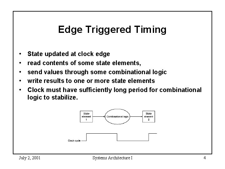
Edge Triggered Timing • • • State updated at clock edge read contents of some state elements, send values through some combinational logic write results to one or more state elements Clock must have sufficiently long period for combinational logic to stabilize. July 2, 2001 Systems Architecture I 4
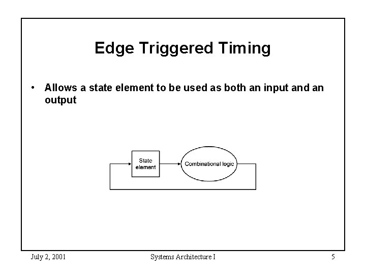
Edge Triggered Timing • Allows a state element to be used as both an input and an output July 2, 2001 Systems Architecture I 5

Components for Simple Implementation • Functional Units needed for each instruction July 2, 2001 Systems Architecture I 6

Register File • A set of registers that can be read/written by supplying a register number to be accessed. • Built using a decoder for each read and write port, and an array of D flip-flops. • For the MIPS processor, the register file has two read ports and one write port. • A write flag is used to indicate that the state should change, and a clock is needed to determine when to change state. July 2, 2001 Systems Architecture I 7
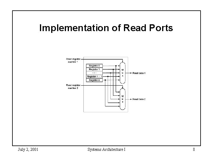
Implementation of Read Ports July 2, 2001 Systems Architecture I 8
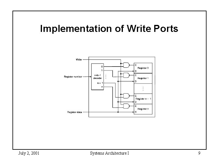
Implementation of Write Ports July 2, 2001 Systems Architecture I 9

Memory • Registers and register files provide the basic building blocks for small memories. • Larger memories are built from SRAMs (Static Random Access Memories) and DRAMs (Dynamic Random Access Memories) • SRAM – – 5 to 25 ns access time largest SRAMs have over 4 Million bits 4 to 6 transistors per bit value stored in cell kept on a pair of inverting gates and can be kept indefinitely • DRAM – 60 to 110 ns access time – 1 transistor per bit – charge stored in capacitor, and needs periodic refreshing July 2, 2001 Systems Architecture I 10

Behavioral Model for Memory library IEEE; use IEEE. std_logic_1164. all; use IEEE. std_logic_arith. all; entity memory is port(address, write_data : in std_logic_vector(31 downto 0); Mem. Write, Mem. Read : in std_logic; read_data : out std_logic_vector(31 downto 0)); end memory; July 2, 2001 Systems Architecture I 11
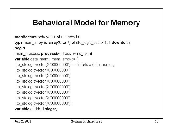
Behavioral Model for Memory architecture behavorial of memory is type mem_array is array(0 to 7) of std_logic_vector (31 downto 0); begin mem_process: process(address, write_data) variable data_mem : mem_array : = ( to_stdlogicvector(X” 0000”), --- initialize data memory to_stdlogicvector(X” 00000000”), to_stdlogicvector(X” 00000000”), to_stdlogicvector(X” 0000”)); variable adddr : integer; July 2, 2001 Systems Architecture I 12
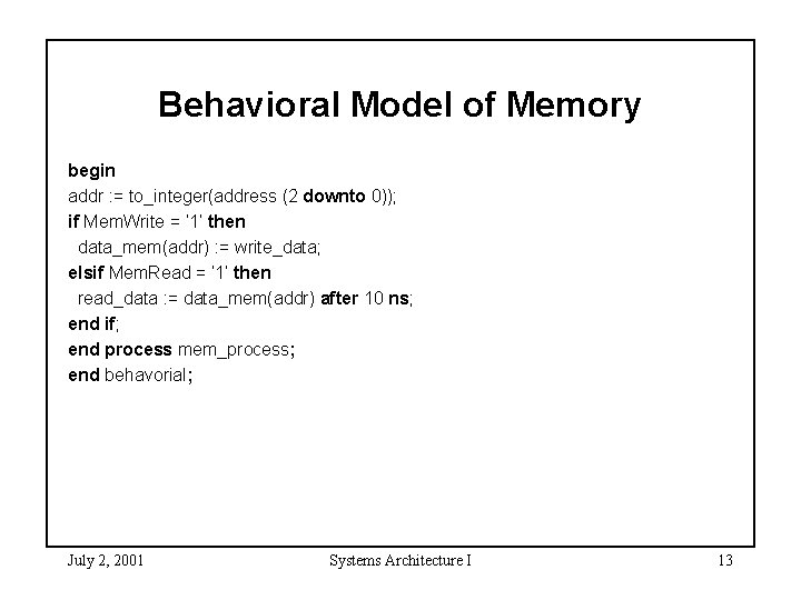
Behavioral Model of Memory begin addr : = to_integer(address (2 downto 0)); if Mem. Write = ‘ 1’ then data_mem(addr) : = write_data; elsif Mem. Read = ‘ 1’ then read_data : = data_mem(addr) after 10 ns; end if; end process mem_process; end behavorial; July 2, 2001 Systems Architecture I 13
- Slides: 13