Systematic approach to PCB interconnects analysis to measurement


Systematic approach to PCB interconnects analysis to measurement validation Marko Marin, Infinera Yuriy Shlepnev, Simberian
Outline • • • Introduction Systematic “sink or swim” validation process Ev. R-1 test board design Measurements and GMS-parameters extraction Board cross-sectioning Material model identification with GMS-parameters Validation: Expectations vs. Reality Conclusion Reality above 30 GHz © 2018 Simberian Inc. 1/16/2022 3
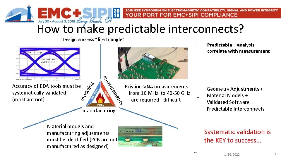
How to make predictable interconnects? Design success “fire triangle” ling de Pristine VNA measurements from 10 MHz to 40 -50 GHz are required - difficult ts en mo rem asu me Accuracy of EDA tools must be systematically validated (most are not) Predictable – analysis correlate with measurement manufacturing Material models and manufacturing adjustments must be identified (PCB are not manufactured as designed) Geometry Adjustments + Material Models + Validated Software = Predictable Interconnects Systematic validation is the KEY to success… 1/16/2022 4

Systematic “sink or swim” validation process 1. 2. 3. 4. 5. 6. Select materials and define PCB stackup with the manufacturer Design test structures with the EM analysis (simple links, launches, vias, …) Manufacture the board, mount connectors (if any) Measure S-parameters and validate quality of the measurements Cross-section the board and identify the manufacturing adjustments (if any) Identify broad-band dielectric and conductor roughness models with GMSparameters or SPP Light techniques 7. Simulate all structures with the identified or validated material models and confirmed adjustments consistently and compare S-parameters and TDR with the measurements (no further manipulations with the data) This presentation is a brief report of lessons learned from such validation… 1/16/2022 5

Ev. R-1 Validation Board “Trust but Validate”
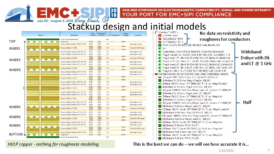
Stackup design and initial models TOP No data on resistivity and roughness for conductors INNER 1 Wideband Debye with Dk and LT @ 1 GHz INNER 2 INNER 3 Half INNER 4 INNER 5 INNER 6 BOTTOM HVLP copper - nothing for roughness modeling This is the best we can do – we will see how accurate it is… 1/16/2022 7
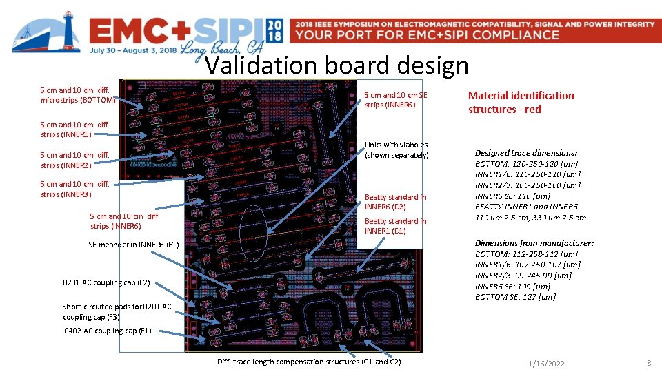
Validation board design 5 cm and 10 cm diff. microstrips (BOTTOM) 5 cm and 10 cm SE strips (INNER 6) Material identification structures - red 5 cm and 10 cm diff. strips (INNER 1) 5 cm and 10 cm diff. strips (INNER 2) 5 cm and 10 cm diff. strips (INNER 3) 5 cm and 10 cm diff. strips (INNER 6) Links with viaholes (shown separately) Beatty standard in INNER 6 (D 2) Beatty standard in INNER 1 (D 1) Designed trace dimensions: BOTTOM: 120 -250 -120 [um] INNER 1/6: 110 -250 -110 [um] INNER 2/3: 100 -250 -100 [um] INNER 6 SE: 110 [um] BEATTY INNER 1 and INNER 6: 110 um 2. 5 cm, 330 um 2. 5 cm Dimensions from manufacturer: BOTTOM: 112 -258 -112 [um] INNER 1/6: 107 -250 -107 [um] INNER 2/3: 99 -245 -99 [um] INNER 6 SE: 109 [um] BOTTOM SE: 127 [um] SE meander in INNER 6 (E 1) 0201 AC coupling cap (F 2) Short-circuited pads for 0201 AC coupling cap (F 3) 0402 AC coupling cap (F 1) Diff. trace length compensation structures (G 1 and G 2) 1/16/2022 8
Post-layout observations • The PCB is manufactured with the “impedance control” process – all trace width and spacing are adjusted by the PCB manufacturer (must be accounted in the analysis) • No information on trace shape (etching) • No reliable information on solder mask shape/parameters • No information on conductor roughness model • No information on actual backdrilling • All this makes analysis inaccurate and practically useless for the target bandwidth

Measurements and GMS-parameters extraction “If measurements do not confirm the model, too bad for the measurements”…
Making pristine measurements from 10 MHz up to 40 GHz is very challenging • • • TDNA, 2. 92 mm connectors (not acceptable for material identification) 27 GHz VNA, 2. 92 mm connectors (failure) 40 GHz VNA, 2. 92 mm connectors (low frequency problem, acceptable) 50 GHz VNA, 2. 4 mm connectors (low frequency problem, acceptable) A few VNA from different vendors evaluated – may be suitable for a separate report… 1/16/2022 11
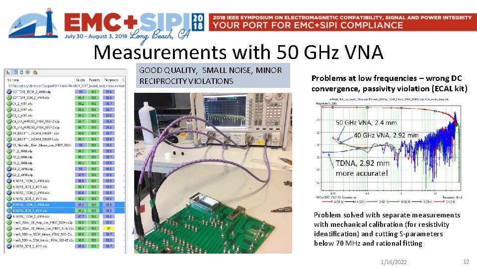
Measurements with 50 GHz VNA GOOD QUALITY, SMALL NOISE, MINOR RECIPROCITY VIOLATIONS Problems at low frequencies – wrong DC convergence, passivity violation (ECAL kit) Problem solved with separate measurements with mechanical calibration (for resistivity identification) and cutting S-parameters below 70 MHz and rational fitting 1/16/2022 12
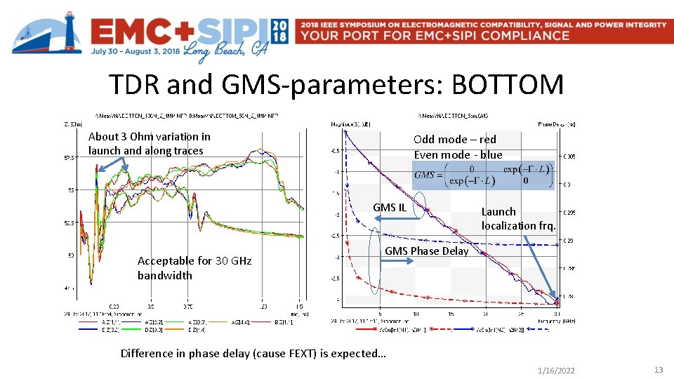
TDR and GMS-parameters: BOTTOM About 3 Ohm variation in launch and along traces Odd mode – red Even mode - blue GMS IL Acceptable for 30 GHz bandwidth Launch localization frq. GMS Phase Delay Difference in phase delay (cause FEXT) is expected… 1/16/2022 13
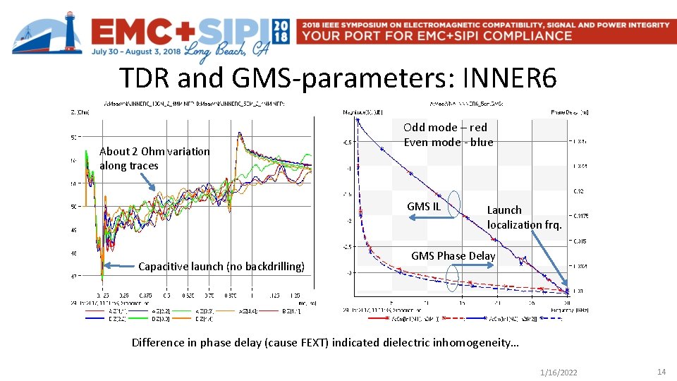
TDR and GMS-parameters: INNER 6 About 2 Ohm variation along traces Odd mode – red Even mode - blue GMS IL Capacitive launch (no backdrilling) Launch localization frq. GMS Phase Delay Difference in phase delay (cause FEXT) indicated dielectric inhomogeneity… 1/16/2022 14

Reality: What is in the board? “What is done by night appears by day”…
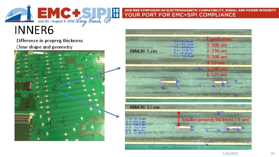
INNER 6 Difference in prepreg thickness Close shape and geometry INNER 6 5 cm Expectations: 1: 108 um 2: 250 um 3: 108 um 4: 15 um 5: 100 um 6: 123 um INNER 6 10 cm Smaller prepreg thickness (-5 um) 1/16/2022 16
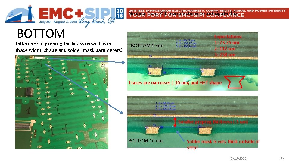
No data from PCB manufacturer to anticipate this BOTTOM Difference in prepreg thickness as well as in thace width, shape and solder mask parameters! BOTTOM 5 cm Expectations: 1: 73. 25 um 2: 112 um 3: 258 um Traces are narrower (-10 um) and HAT shape Smaller prepreg thickness (-3 um) BOTTOM 10 cm Solder mask is very thick outside of strip! 1/16/2022 17
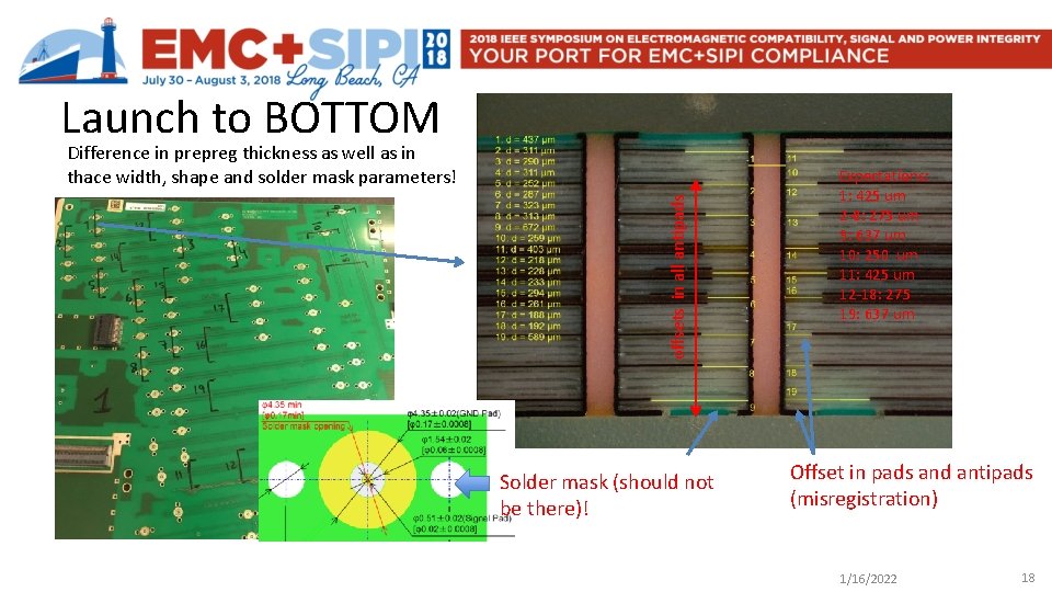
Launch to BOTTOM offsets in all antipads Difference in prepreg thickness as well as in thace width, shape and solder mask parameters! Solder mask (should not be there)! Expectations: 1: 425 um 2 -8: 275 um 9: 637 um 10: 250 um 11: 425 um 12 -18: 275 19: 637 um Offset in pads and antipads (misregistration) 1/16/2022 18
![Final trace geometry adjustments Designed trace dimensions: BOTTOM: 120 -250 -120 [um] INNER 1/6: Final trace geometry adjustments Designed trace dimensions: BOTTOM: 120 -250 -120 [um] INNER 1/6:](http://slidetodoc.com/presentation_image_h2/77d87cec30e87c89eac6d588a902e3e0/image-19.jpg)
Final trace geometry adjustments Designed trace dimensions: BOTTOM: 120 -250 -120 [um] INNER 1/6: 110 -250 -110 [um] INNER 2/3: 100 -250 -100 [um] INNER 6 SE: 110 [um] BEATTY INNER 1 and INNER 6: 110 um 2. 5 cm, 330 um 2. 5 cm Dimensions from manufacturer: BOTTOM: 112 -258 -112 [um] INNER 1/6: 107 -250 -107 [um] INNER 2/3: 99 -245 -99 [um] INNER 6 SE: 109 [um] Dimensions after cross-sectioning: BOTTOM: HAT(89/97)-260 -HAT(89/97) [um] INNER 1/6: 107 -255 -107 [um] INNER 2/3: 96 -254 -96 [um] INNER 6 SE: 109 [um] BEATTY INNER 6: 109 um 2. 5 cm + 326 um 2. 5 cm Thickness of prepreg layers is reduced by 3 -5 um – it is almost the same thickness as for the core (it should be) Microstrip layer metal thickness is 48 um instead of 35 um Solder mask layer – 10 um over strips and 38 um between the strips! These ones are very critical! Parameters for strip layers are closer to expectations 1/16/2022 19

Material Model Identification Done with GMS-parameters in Simbeor
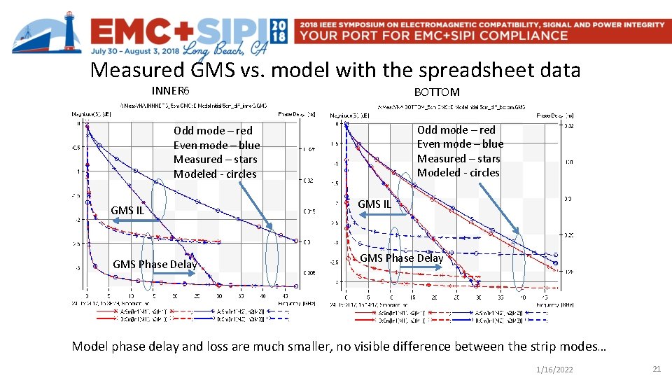
Measured GMS vs. model with the spreadsheet data INNER 6 BOTTOM Odd mode – red Even mode – blue Measured – stars Modeled - circles GMS IL GMS Phase Delay Model phase delay and loss are much smaller, no visible difference between the strip modes… 1/16/2022 21
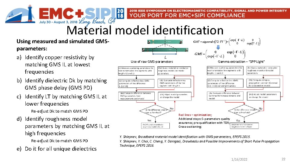
Material model identification Using measured and simulated GMSparameters: a) Identify copper resistivity by matching GMS IL at lowest frequencies b) Identify dielectric Dk by matching GMS phase delay (GMS PD) c) Identify LT by matching GMS IL at lower frequencies Re-adjust Dk to match GMS PD d) Identify roughness model parameters by matching GMS IL at high frequencies Re-adjust Dk to match GMS PD e) Do it for all unique dielectrics L Use of raw GMS-parameters Gamma extraction – “SPP Light” Red lines – optimization; Additional steps: S-parameters quality assurance; pre-qualification with TDR; Cross-sectioning; Y. Shlepnev, Broadband material model identification with GMS-parameters, EPEPS 2015. Y. Shlepnev, Y. Choi, C. Cheng, Y. Damgaci, Drawbacks and Possible Improvements of Short Pulse Propagation Technique, EPEPS 2016. 1/16/2022 22
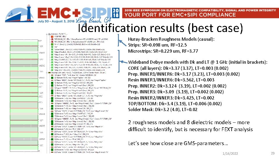
Identification results (best case) Huray-Bracken Roughness Models (causal): Strips: SR=0. 098 um, RF=12. 5 Microstrips: SR=0. 229 um, RF=3. 77 Wideband Debye models with Dk and LT @ 1 GHz (initial in brackets): CORE (all layers): Dk=3. 37 (3. 37), LT=0. 003 (0. 002) Prep. INNER 1/INNER 6: Dk=3. 17 (3. 23), LT=0. 003 (0. 002) Resin INNER 1/INNER 6: Dk=3. 562, LT=0. 003 Prep. INNER 2: Dk=3. 124 (3. 19), LT=0. 002 (0. 002) Prep. INNER 3: Dk=3. 09 (3. 19), LT=0. 002 (0. 002) Resin INNER 2/INNER 3: Dk=3. 425, LT=0. 002 TOP/BOTTOM: Dk=3. 4 (3. 19), LT=0. 006 (0. 002) Solder Mask: Dk=3. 2 (4. 0), LT=0. 02 2 roughness models and 8 dielectric models – more difficult to identify, but is necessary for FEXT analysis Let’s see how close are GMS-parameters… 1/16/2022 23
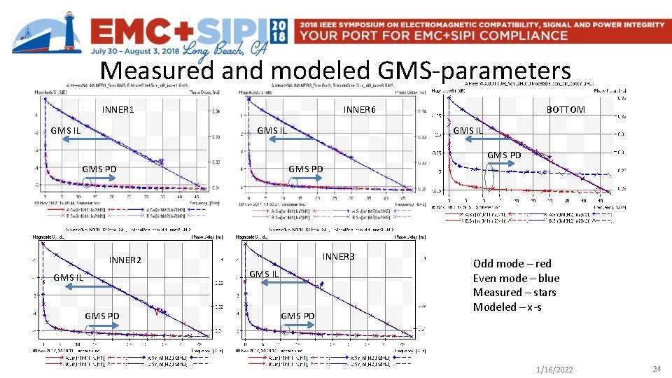
Measured and modeled GMS-parameters INNER 1 GMS IL INNER 6 GMS IL BOTTOM GMS IL GMS PD INNER 3 INNER 2 GMS IL GMS PD Odd mode – red Even mode – blue Measured – stars Modeled – x-s 1/16/2022 24
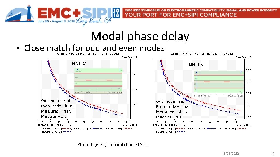
Modal phase delay • Close match for odd and even modes INNER 2 Odd mode – red Even mode – blue Measured – stars Modeled – x-s INNER 6 Odd mode – red Even mode – blue Measured – stars Modeled – x-s Should give good match in FEXT… 1/16/2022 25

Validation: Expectations vs. Reality “The Moment of Truth”…
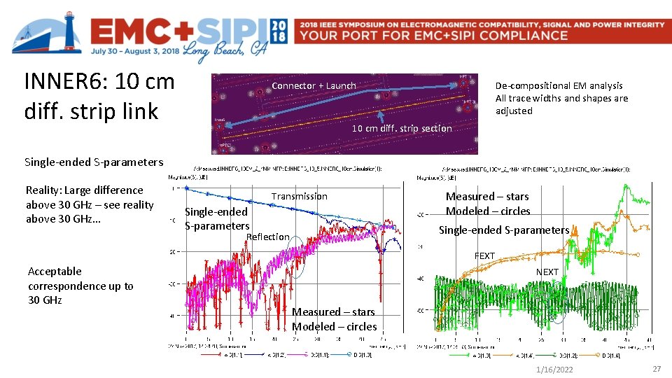
INNER 6: 10 cm diff. strip link De-compositional EM analysis All trace widths and shapes are adjusted Connector + Launch 10 cm diff. strip section Single-ended S-parameters Reality: Large difference above 30 GHz – see reality above 30 GHz… Transmission Single-ended S-parameters Measured – stars Modeled – circles Single-ended S-parameters Reflection FEXT Acceptable correspondence up to 30 GHz NEXT Measured – stars Modeled – circles 1/16/2022 27
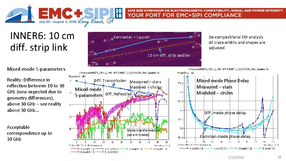
INNER 6: 10 cm diff. strip link Connector + Launch De-compositional EM analysis All trace widths and shapes are adjusted 10 cm diff. strip section Mixed-mode S-parameters Reality: Difference in reflection between 10 to 30 GHz (now expected due to geometry differences), above 30 GHz – see reality above 30 GHz… Acceptable correspondence up to 30 GHz Diff. Transmission Measured – stars Modeled – circles Mixed-mode S-parameters Diff. Reflection Mixed-mode Phase Delay Measured – stars Modeled – circles Diff. mode phase delay Mode transformations (zero in model) Common mode phase delay 1/16/2022 28
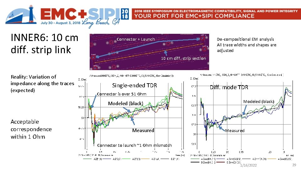
INNER 6: 10 cm diff. strip link Reality: Variation of impedance along the traces (expected) Connector + Launch De-compositional EM analysis All trace widths and shapes are adjusted 10 cm diff. strip section Single-ended TDR Connector is over 51 Ohm Modeled (black) Acceptable correspondence within 1 Ohm Measured Diff. mode TDR Modeled (black) Measured Connector to launch ~1 Ohm mismatch 1/16/2022 29
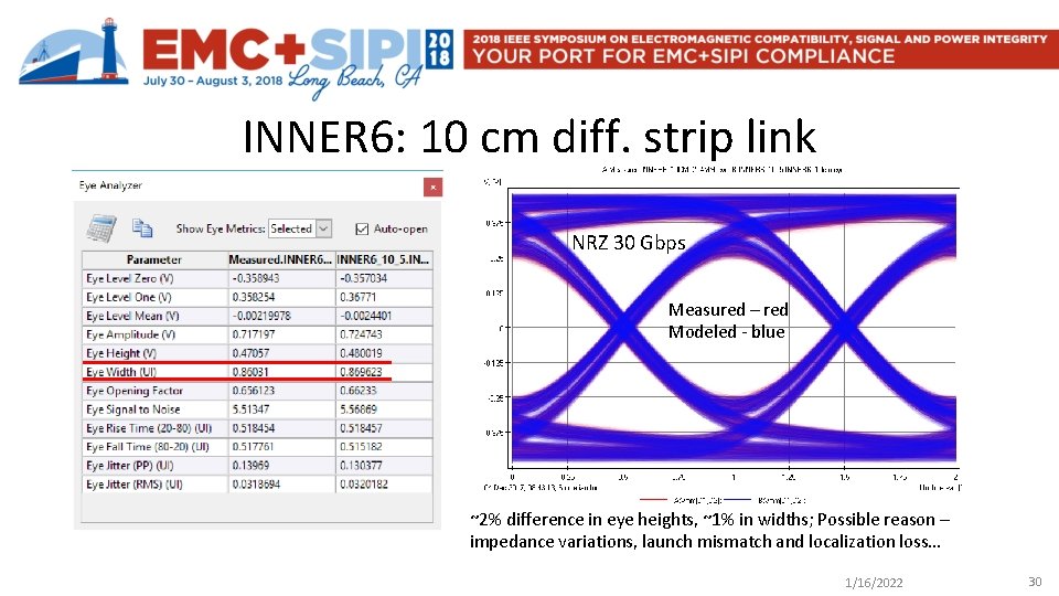
INNER 6: 10 cm diff. strip link NRZ 30 Gbps Measured – red Modeled - blue ~2% difference in eye heights, ~1% in widths; Possible reason – impedance variations, launch mismatch and localization loss… 1/16/2022 30
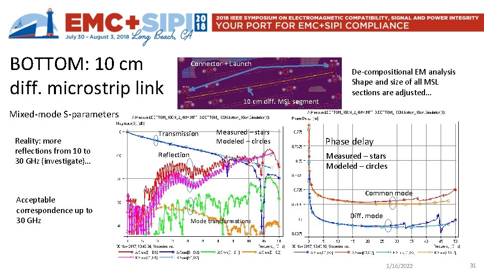
BOTTOM: 10 cm diff. microstrip link Connector + Launch 10 cm diff. MSL segment De-compositional EM analysis Shape and size of all MSL sections are adjusted… Mixed-mode S-parameters Reality: more reflections from 10 to 30 GHz (investigate)… Acceptable correspondence up to 30 GHz Transmission Measured – stars Modeled – circles Reflection Phase delay Measured – stars Modeled – circles Common mode Mode transformations Diff. mode 1/16/2022 31
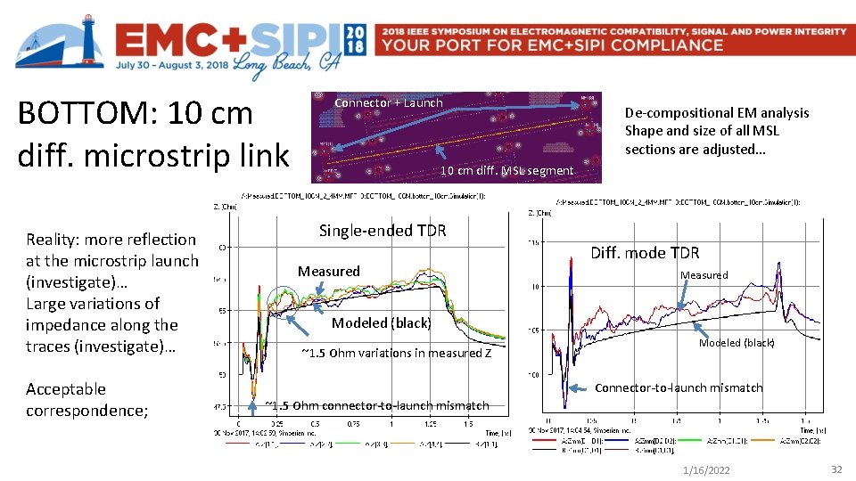
BOTTOM: 10 cm diff. microstrip link Reality: more reflection at the microstrip launch (investigate)… Large variations of impedance along the traces (investigate)… Acceptable correspondence; Connector + Launch De-compositional EM analysis Shape and size of all MSL sections are adjusted… 10 cm diff. MSL segment Single-ended TDR Measured Diff. mode TDR Measured Modeled (black) ~1. 5 Ohm variations in measured Z Modeled (black) Connector-to-launch mismatch ~1. 5 Ohm connector-to-launch mismatch 1/16/2022 32
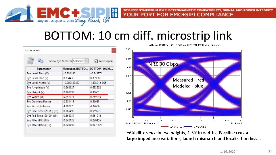
BOTTOM: 10 cm diff. microstrip link NRZ 30 Gbps Measured – red Modeled - blue ~6% difference in eye heights, 1. 5% in widths; Possible reason – large impedance variations, launch mismatch and localization loss… 1/16/2022 33
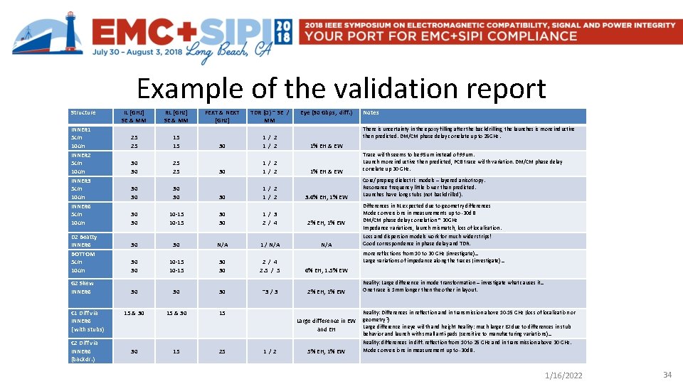
Example of the validation report Structure INNER 1 5 cm 10 cm INNER 2 5 cm 10 cm INNER 3 5 cm 10 cm INNER 6 5 cm 10 cm D 2 Beatty INNER 6 BOTTOM 5 cm 10 cm G 2 Skew INNER 6 C 1 Diff via INNER 6 ( with stubs) C 2 Diff via INNER 6 (backdr. ) IL [GHz] SE & MM 25 25 30 30 RL [GHz] SE & MM 15 15 25 25 30 30 FEXT & NEXT [GHz] 30 30 30 TDR (Ω) ~ SE / MM 1 / 2 1 / 2 Eye (30 Gbps, diff. ) There is uncertainty in the epoxy filling after the backdrilling, the launches is more inductive then predicted. DM/CM phase delay correlate up to 25 GHz. 1% EH & EW 3. 6% EH, 1% EW 30 30 10 -15 30 30 1 / 3 2 / 4 2% EH, 1% EW 30 30 N/A 1 / N/A 30 30 10 -15 30 30 2 / 4 2. 5 / 5 6% EH, 1. 5% EW 30 30 30 ~3 / 3 2% EH, 1% EW 15 & 30 15 15 25 1 /2 Trace width seems to be 95 um instead of 99 um. Launch more inductive then predicted, PCB trace width variation. DM/CM phase delay correlate up 30 GHz. Core/prepreg dielectric models – layered anisotropy. Resonance frequency little lower than predicted. Launches have long stubs (not backdrilled). Differences in RL expected due to geometry differences Mode conversions in measurements up to -30 d. B DM/CM phase delay correlation ~ 30 GHz Impedance variations, launch mismatch, loss of localization. Loss and dispersion models work for much wider strips! Good correspondence in phase delay and TDR. more reflections from 10 to 30 GHz (investigate)… Large variations of impedance along the traces (investigate)… Large difference in EW and EH 30 Notes 5% EH, 1% EW Reality: Large difference in mode transformation – investigate what causes it… One trace is 1 mm longer then the other in layout. Reality: Differences in reflection and in transmission above 10 -15 GHz (loss of localization or geometry? ) Large difference in eye width and height Reality: much larger ISI due to differences in stub behavior and launch with small anti-pads (sensitive to manufacturing variations)… Reality: differences in diff. reflection from 10 to 25 GHz and in transmission above 30 GHz. Mode conversions in measurement up to -30 d. B. 1/16/2022 34
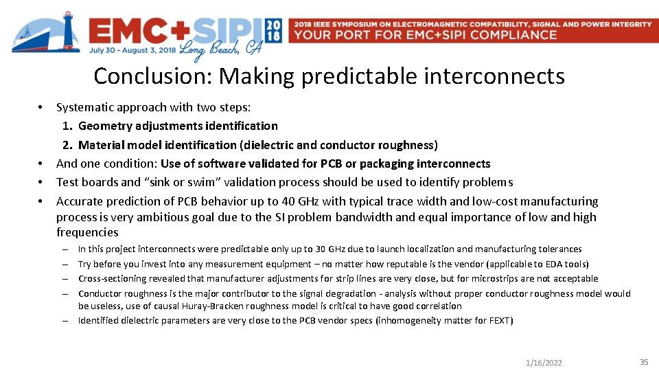
Conclusion: Making predictable interconnects • • Systematic approach with two steps: 1. Geometry adjustments identification 2. Material model identification (dielectric and conductor roughness) And one condition: Use of software validated for PCB or packaging interconnects Test boards and “sink or swim” validation process should be used to identify problems Accurate prediction of PCB behavior up to 40 GHz with typical trace width and low-cost manufacturing process is very ambitious goal due to the SI problem bandwidth and equal importance of low and high frequencies In this project interconnects were predictable only up to 30 GHz due to launch localization and manufacturing tolerances Try before you invest into any measurement equipment – no matter how reputable is the vendor (applicable to EDA tools) Cross-sectioning revealed that manufacturer adjustments for strip lines are very close, but for microstrips are not acceptable Conductor roughness is the major contributor to the signal degradation - analysis without proper conductor roughness model would be useless, use of causal Huray-Bracken roughness model is critical to have good correlation – Identified dielectric parameters are very close to the PCB vendor specs (inhomogeneity matter for FEXT) – – 1/16/2022 35

Reality above 30 GHz “So many blissful revelations The spirit of enlightment hides!”. . .
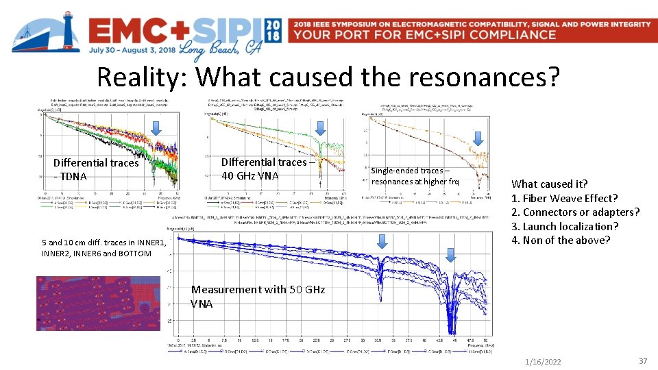
Reality: What caused the resonances? Differential traces - TDNA Differential traces – 40 GHz VNA 5 and 10 cm diff. traces in INNER 1, INNER 2, INNER 6 and BOTTOM Single-ended traces – resonances at higher frq What caused it? 1. Fiber Weave Effect? 2. Connectors or adapters? 3. Launch localization? 4. Non of the above? Measurement with 50 GHz VNA 1/16/2022 37
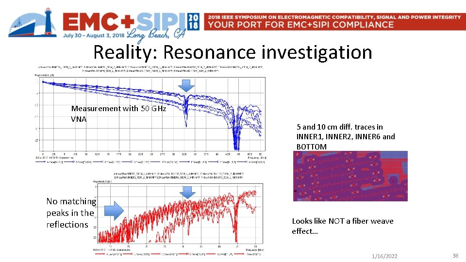
Reality: Resonance investigation Measurement with 50 GHz VNA No matching peaks in the reflections 5 and 10 cm diff. traces in INNER 1, INNER 2, INNER 6 and BOTTOM Looks like NOT a fiber weave effect… 1/16/2022 38
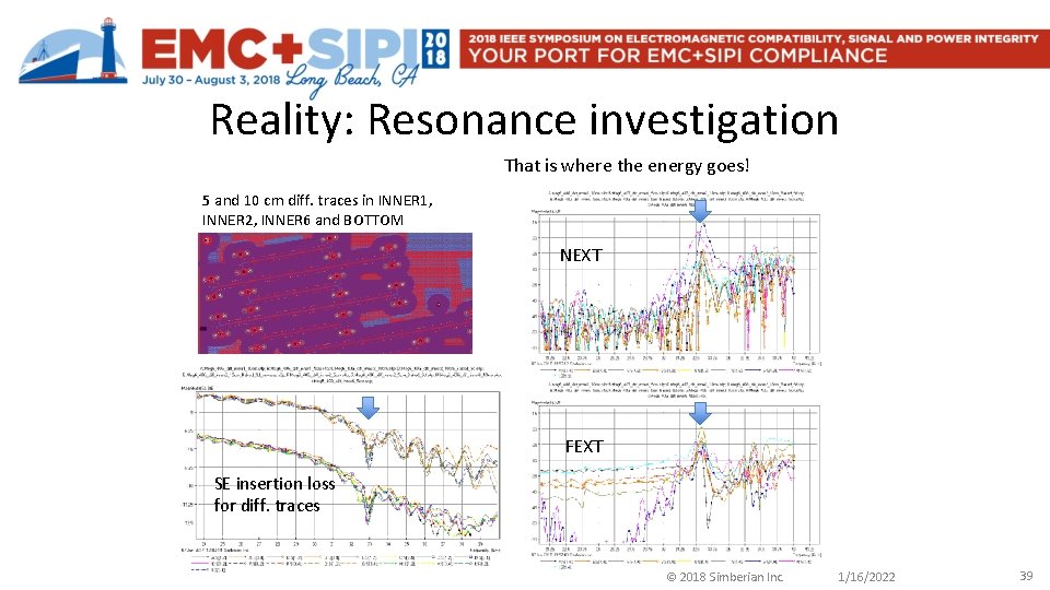
Reality: Resonance investigation That is where the energy goes! 5 and 10 cm diff. traces in INNER 1, INNER 2, INNER 6 and BOTTOM NEXT FEXT SE insertion loss for diff. traces © 2018 Simberian Inc. 1/16/2022 39
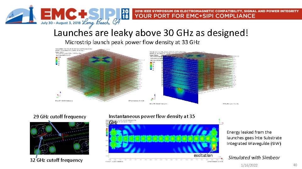
Launches are leaky above 30 GHz as designed! Microstrip launch peak power flow density at 33 GHz 29 GHz cutoff frequency Instantaneous power flow density at 35 GHz Energy leaked from the launches goes into Substrate Integrated Waveguide (SIW) 32 GHz cutoff frequency excitation Simulated with Simbeor 1/16/2022 40
- Slides: 40