
Synchronous Latency Insensitive Design Christer Svensson and Anders
- Slides: 37
Synchronous Latency Insensitive Design Christer Svensson and Anders Edman Linköping University With contributions by Behzad Mesgarzadeh and Peter Caputa Christer Svensson, Marstrand 2005 1
Outline • • Introduction A comment on wires Architectural view of future systems Synchronous Latency Insensitive Design Multiple clocks Unmatched buses Conclusion Christer Svensson, Marstrand 2005 2
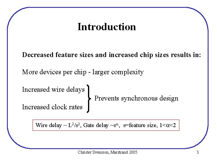
Introduction Decreased feature sizes and increased chip sizes results in: More devices per chip - larger complexity Increased wire delays Prevents synchronous design Increased clock rates Wire delay ~ L 2/s 2, Gate delay ~sa, s=feature size, 1<a<2 Christer Svensson, Marstrand 2005 3
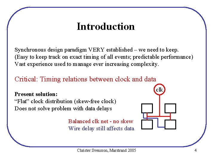
Introduction Synchronous design paradigm VERY established – we need to keep. (Easy to keep track on exact timing of all events; predictable performance) Vast experience used to manage ever increasing complexity. Critical: Timing relations between clock and data Present solution: “Flat” clock distribution (skew-free clock) Does not solve problem with data delays clk Balanced clk net - no skew Wire delay still affects data Christer Svensson, Marstrand 2005 4
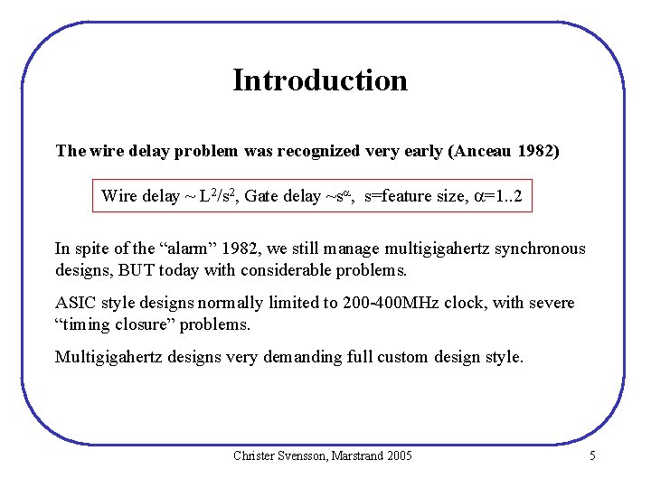
Introduction The wire delay problem was recognized very early (Anceau 1982) Wire delay ~ L 2/s 2, Gate delay ~sa, s=feature size, a=1. . 2 In spite of the “alarm” 1982, we still manage multigigahertz synchronous designs, BUT today with considerable problems. ASIC style designs normally limited to 200 -400 MHz clock, with severe “timing closure” problems. Multigigahertz designs very demanding full custom design style. Christer Svensson, Marstrand 2005 5
Introduction “Classical” methods to manage: Asynchronous communication between blocks FCPU (Lawson et. al. 1974) Global asynchronous local synchronous (GALS) Low frequency communication clock (Anceau 1982) Skew-free clock distribution and pipelined buses (eg. Intel microprocessors) Christer Svensson, Marstrand 2005 6
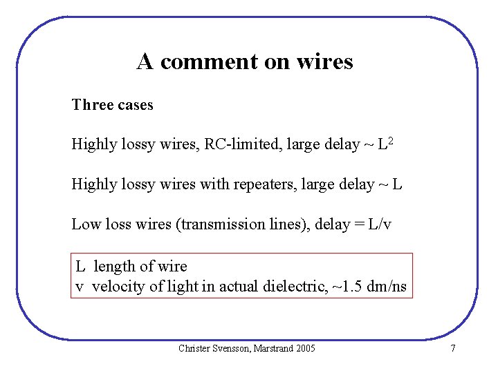
A comment on wires Three cases Highly lossy wires, RC-limited, large delay ~ L 2 Highly lossy wires with repeaters, large delay ~ L Low loss wires (transmission lines), delay = L/v L length of wire v velocity of light in actual dielectric, ~1. 5 dm/ns Christer Svensson, Marstrand 2005 7
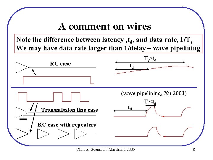
A comment on wires Note the difference between latency , td, and data rate, 1/Ts We may have data rate larger than 1/delay – wave pipelining RC case td Transmission line case Ts>td (wave pipelining, Xu 2003) Ts<td td RC case with repeaters Christer Svensson, Marstrand 2005 8
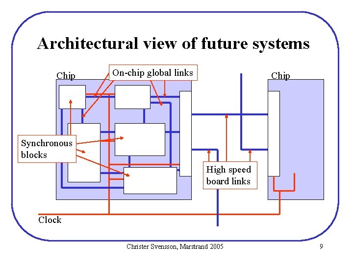
Architectural view of future systems Chip On-chip global links Chip Synchronous blocks High speed board links Clock Christer Svensson, Marstrand 2005 9
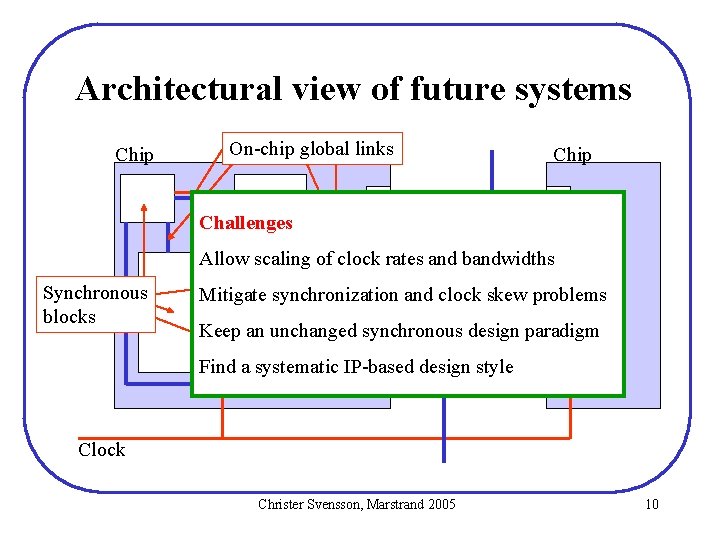
Architectural view of future systems Chip On-chip global links Chip Challenges Allow scaling of clock rates and bandwidths Synchronous blocks Mitigate synchronization and clock skew problems Keep an unchanged synchronous design paradigm High speed Find a systematic IP-based design style board links Clock Christer Svensson, Marstrand 2005 10
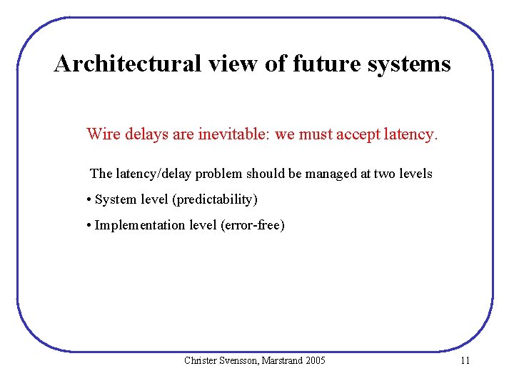
Architectural view of future systems Wire delays are inevitable: we must accept latency. The latency/delay problem should be managed at two levels • System level (predictability) • Implementation level (error-free) Christer Svensson, Marstrand 2005 11
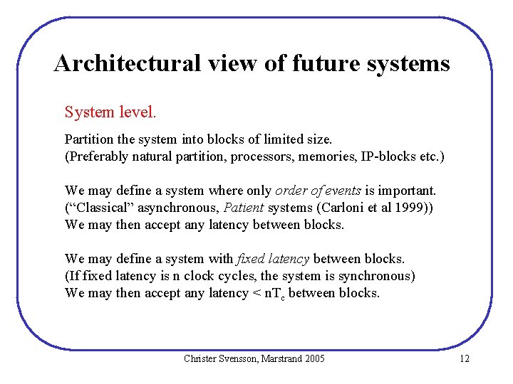
Architectural view of future systems System level. Partition the system into blocks of limited size. (Preferably natural partition, processors, memories, IP-blocks etc. ) We may define a system where only order of events is important. (“Classical” asynchronous, Patient systems (Carloni et al 1999)) We may then accept any latency between blocks. We may define a system with fixed latency between blocks. (If fixed latency is n clock cycles, the system is synchronous) We may then accept any latency < n. Tc between blocks. Christer Svensson, Marstrand 2005 12
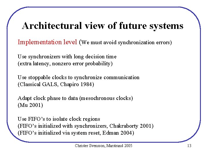
Architectural view of future systems Implementation level (We must avoid synchronization errors) Use synchronizers with long decision time (extra latency, nonzero error probability) Use stoppable clocks to synchronize communication (Classical GALS, Chapiro 1984) Adapt clock phase to data (mesochronous clocks) (Mu 2001) Use FIFO’s to isolate clock regions (FIFO’s initialized with synchronizers, Chakraborty 2001) (FIFO’s initialized via system reset, Edman 2004) Christer Svensson, Marstrand 2005 13
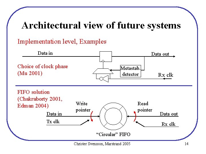
Architectural view of future systems Implementation level, Examples Data in Data out Choice of clock phase (Mu 2001) FIFO solution (Chakraborty 2001, Edman 2004) Data in Tx clk Metastab. detector Write pointer Read pointer Rx clk Data out Rx clk “Circular” FIFO Christer Svensson, Marstrand 2005 14
Synchronous Latency Insensitive Design Problem formulation Find a method to mitigate wire-induced latencies within a synchronous paradigm Christer Svensson, Marstrand 2005 15
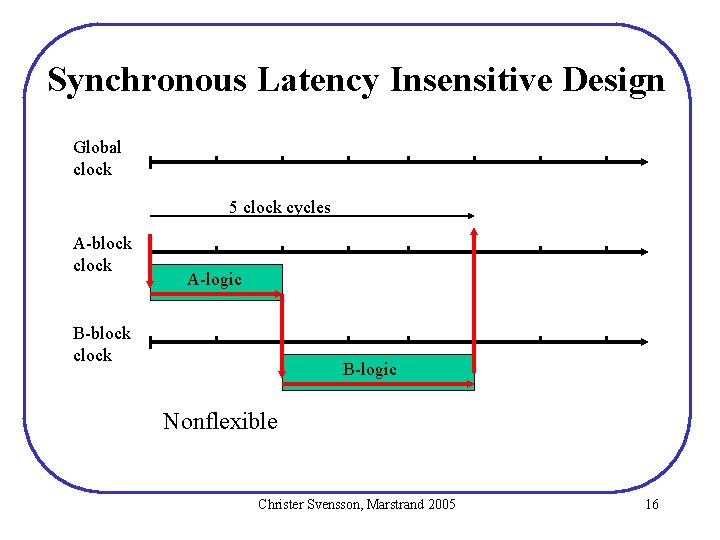
Synchronous Latency Insensitive Design Global clock 5 clock cycles A-block clock A-logic B-block clock B-logic Nonflexible Christer Svensson, Marstrand 2005 16
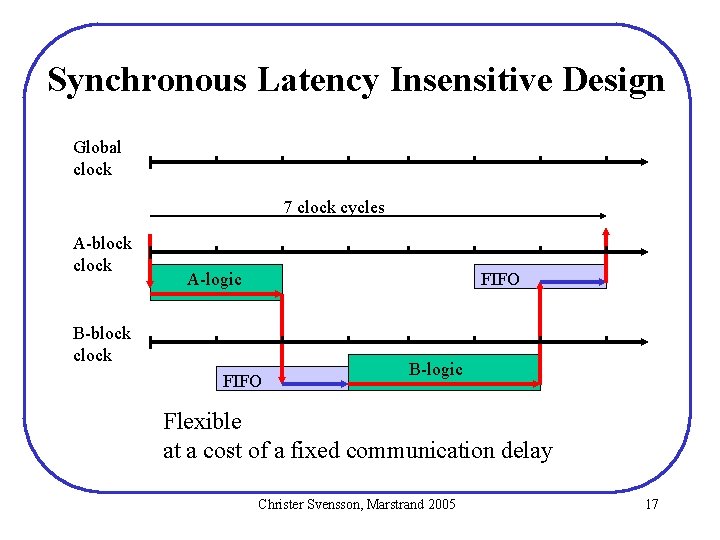
Synchronous Latency Insensitive Design Global clock 7 clock cycles A-block clock A-logic FIFO B-block clock FIFO B-logic Flexible at a cost of a fixed communication delay Christer Svensson, Marstrand 2005 17
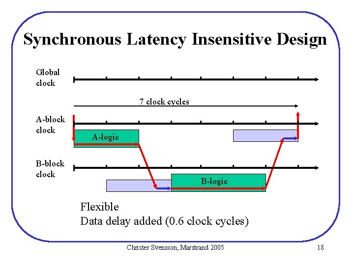
Synchronous Latency Insensitive Design Global clock 7 clock cycles A-block clock B-block clock A-logic B-logic Flexible Data delay added (0. 6 clock cycles) Christer Svensson, Marstrand 2005 18
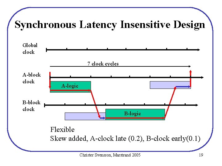
Synchronous Latency Insensitive Design Global clock 7 clock cycles A-block clock B-block clock A-logic B-logic Flexible Skew added, A-clock late (0. 2), B-clock early(0. 1) Christer Svensson, Marstrand 2005 19
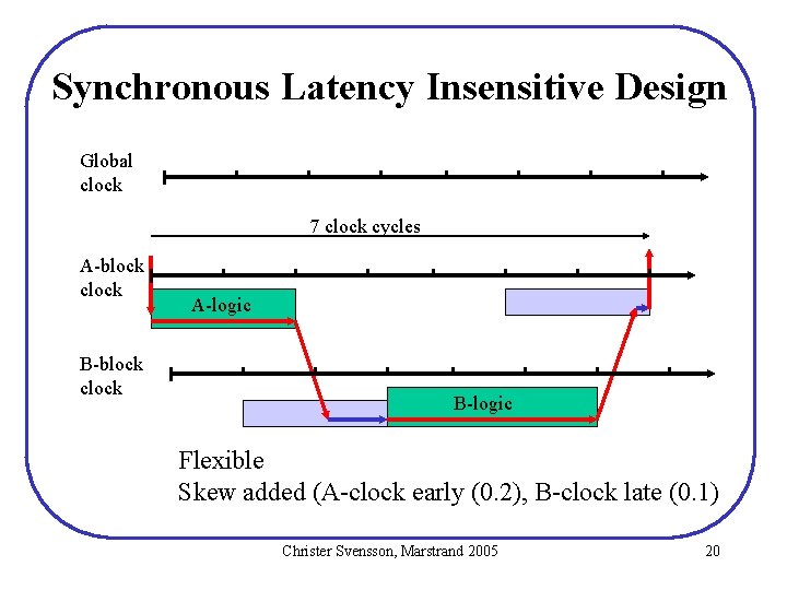
Synchronous Latency Insensitive Design Global clock 7 clock cycles A-block clock B-block clock A-logic B-logic Flexible Skew added (A-clock early (0. 2), B-clock late (0. 1) Christer Svensson, Marstrand 2005 20
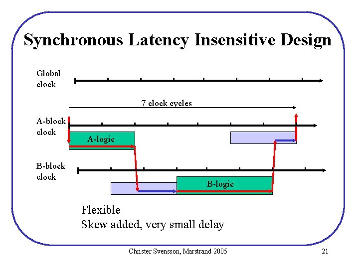
Synchronous Latency Insensitive Design Global clock 7 clock cycles A-block clock B-block clock A-logic B-logic Flexible Skew added, very small delay Christer Svensson, Marstrand 2005 21
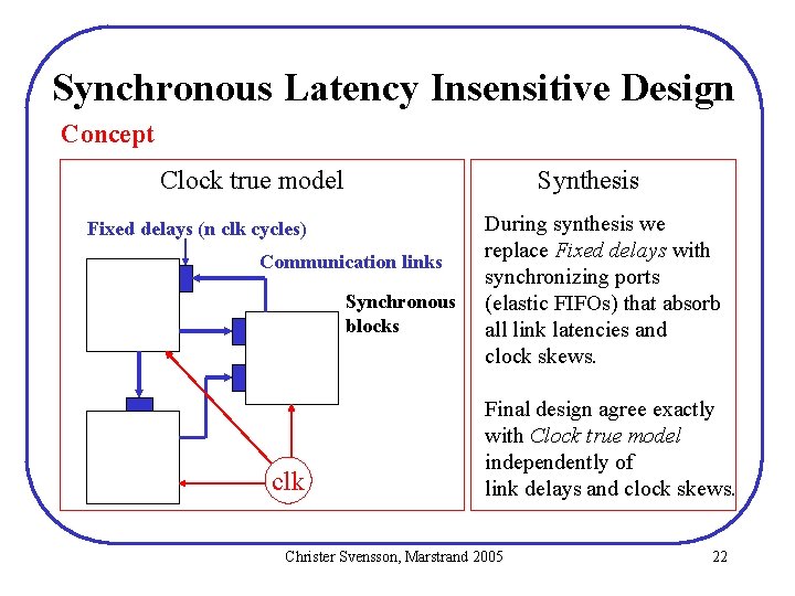
Synchronous Latency Insensitive Design Concept Clock true model Synthesis Fixed delays (n clk cycles) Communication links Synchronous blocks clk During synthesis we replace Fixed delays with synchronizing ports (elastic FIFOs) that absorb all link latencies and clock skews. Final design agree exactly with Clock true model independently of link delays and clock skews. Christer Svensson, Marstrand 2005 22
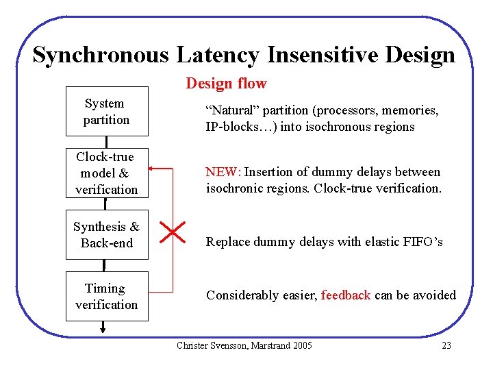
Synchronous Latency Insensitive Design flow System partition “Natural” partition (processors, memories, IP-blocks…) into isochronous regions Clock-true model & verification NEW: Insertion of dummy delays between isochronic regions. Clock-true verification. Synthesis & Back-end Replace dummy delays with elastic FIFO’s Timing verification Considerably easier, feedback can be avoided Christer Svensson, Marstrand 2005 23
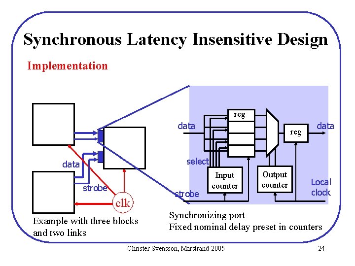
Synchronous Latency Insensitive Design Implementation reg data select data strobe clk Example with three blocks and two links strobe Input counter Output counter Local clock Synchronizing port Fixed nominal delay preset in counters Christer Svensson, Marstrand 2005 24
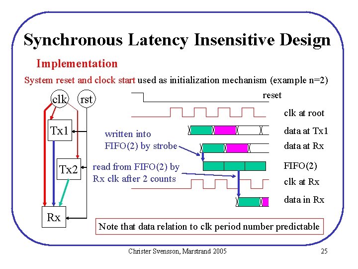
Synchronous Latency Insensitive Design Implementation System reset and clock start used as initialization mechanism (example n=2) reset clk rst clk at root Tx 1 Tx 2 written into FIFO(2) by strobe read from FIFO(2) by Rx clk after 2 counts data at Tx 1 data at Rx FIFO(2) clk at Rx data in Rx Rx Note that data relation to clk period number predictable Christer Svensson, Marstrand 2005 25
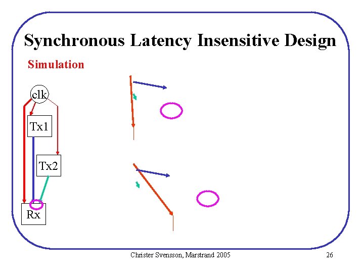
Synchronous Latency Insensitive Design Simulation clk Tx 1 Tx 2 Rx Christer Svensson, Marstrand 2005 26
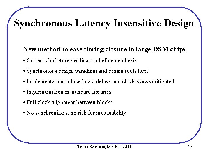
Synchronous Latency Insensitive Design New method to ease timing closure in large DSM chips • Correct clock-true verification before synthesis • Synchronous design paradigm and design tools kept • Implementation induced data delays and clock skews mitigated • Implementation in standard libraries • Full clock alignment between blocks • No synchronizers, no risk for metastability Christer Svensson, Marstrand 2005 27
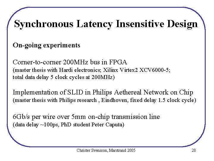
Synchronous Latency Insensitive Design On-going experiments Corner-to-corner 200 MHz bus in FPGA (master thesis with Hardi electronics; Xilinx Virtex 2 XCV 6000 -5; total data delay 5 clock cycles at 200 MHz) Implementation of SLID in Philips Aethereal Network on Chip (master thesis with Philips research , Eindhoven, fixed delay 1. 5 clock cycle) 6 Gb/s per wire over 5 mm on-chip transmission line (data delay ~100 ps, Ph. D student Peter Caputa) Christer Svensson, Marstrand 2005 28
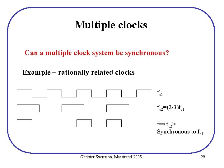
Multiple clocks Can a multiple clock system be synchronous? Example – rationally related clocks fc 1 fc 2=(2/3)fc 1 f=<fc 2> Synchronous to fc 1 Christer Svensson, Marstrand 2005 29
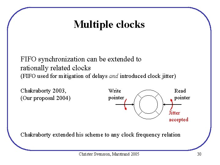
Multiple clocks FIFO synchronization can be extended to rationally related clocks (FIFO used for mitigation of delays and introduced clock jitter) Chakraborty 2003, (Our proposal 2004) Write pointer Read pointer Jitter accepted Chakraborty extended his scheme to any clock frequency relation Christer Svensson, Marstrand 2005 30
Multiple clocks Global reset used for initialization Distributed along slow global clock and resynchronized locally Local clock generated by PLL flocal = n*fglobal Frequency adjust with rate multipliers Highest frequency reduced to average of lower frequency Christer Svensson, Marstrand 2005 31
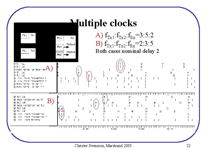
Multiple clocks A) f. Tx 1: f. Tx 2: f. Rx=3: 5: 2 B) f. Tx 1: f. Tx 2: f. Rx=2: 3: 5 Both cases nominal delay 2 A) B) Christer Svensson, Marstrand 2005 32
Unmatched buses The proposed schemes depends on a matched bus, That is data bits and strobe have equal delay Can we extend this scheme to an unmatched bus? Motivations: Long buses in ASIC or FPGA may have matching problem, it tools do not support matching. In chip-to-chip communication, wire length matching is tricky due to package or backplane contacts do not fit board bus width Christer Svensson, Marstrand 2005 33
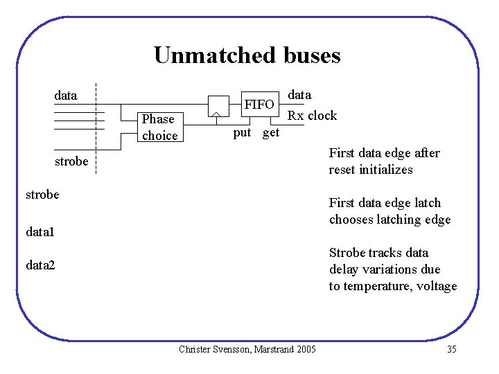
Unmatched buses Need to solve two problems: Phase alignment of latching receiver clock to arriving data Individual FIFO initialization per bit (can not use strobe) Christer Svensson, Marstrand 2005 34
Unmatched buses data Phase choice FIFO data Rx clock put get First data edge after reset initializes strobe First data edge latch chooses latching edge data 1 Strobe tracks data delay variations due to temperature, voltage data 2 Christer Svensson, Marstrand 2005 35
Conclusions Wire delays are inevitable Delays must be managed at system level and implementation level Our proposed scheme facilitates: synchronous flow from system to implementation clock-true verification before synthesis mitigation of clock skews and data latencies Our scheme can be extended to multiple clock frequencies Our scheme can be extended to unmatched buses Christer Svensson, Marstrand 2005 36
References F. Anceau, "A Synchronous Approach for Clocking VLSI Systems", IEEE J. Solid-State Circuits, Vol. 17, pp. 51 -56, 1982. D. M. Chapiro, “Globally-Asynchronous Locally-Synchronous Systems”, Ph. D Thesis, Stanford University, Oct. 1984. D. Sylvester and K. Keutzer, "Getting to the bottom of deep submicron", IEEE/ACM Int. Conference on Computer Aided Design 1998, Digest of Technical Papers, pp. 203 -211, 1998. L. P. Carloni, K. L. Mc. Millan, A. Saldanha and A. L. Sangiovanni-Vincentelli, "A Methodology for Correct-by-Construction Latency Insensitive Design", 1999 IEEE/ACM International Conference on Computer-Aided Design, Digest of Technical Papers, pp. 309 -315, Nov. 1999. F. Mu and C. Svensson, ”Self-tested self-synchronization circuit for mesochronous clocking”, IEEE Trans. on Circuits and Systems II: Analog and Digital Signal Processing, vol 48, pp. 129 – 140, Feb. 2001 C. Svensson, “Electrical Interconnects Revitalized”, IEEE Trans. on Very Large Scale Integration, vol. 10, pp. 777 -788, Dec. 2002. J. Xu and W. Wolf, “A Wave-Pipelined On-chip Interconnect Structure for Network-on-Chips”, Proc. of the 11 th Symp. On High Performance Interconnect, pp. 10 -14, 2003 A. Chakraborty and M. R. Greenstreet, “Efficient Self-Timed Interfaces for Crossing Clock Domains”, Proceedings of Ninth International Symposium on Asynchronous Circuits and Systems, pp. 78 -88, May 2003. C. Svensson, "Synchronous Latency Insensitive Design", invited paper, The 10 th IEEE International Symposium on Asynchronous Circuits and Systems, Crete, April 19 -23, 2004. A. Edman and C. Svensson, "Timing Closure through a Globally Synchronous, Timing Partitioned Design Methodology", Proc of the 41 st Design Automation Conference, pp. 71 -74, June 2004. Christer Svensson, Marstrand 2005 37