Synchronous Digital Design Methodology and Guidelines Digital System


- Slides: 26
Synchronous Digital Design Methodology and Guidelines Digital System Design
What is Synchronous Design and Why? Rules • All flip-flops clocked by one common clock • Reset only used for initialization Advantages • • Races and hazards are no problem Simple design methodology Wide EDA tool support Simple DFT
Timing Hazard • Static hazard: possibility of a brief signal value change when the signal was expected to be stable, due to timing (glitch) • Dynamic hazard: possibility of multiple output transitions caused by a single input transition due to multiple signal paths with different delays
Static Hazard If d is the delay of each gate
Analyzing Static Hazards using Karnaugh maps A static hazard can occur when changing a single input variable causes a jump from one prime implicant to another Solution: include an additional prime implicant
Eliminating hazards using Flip. Flops
Synchronous Design • Three things must be ensured by the designer: – Minimize and determine clock skew – Account for flip-flop setup and hold times – Reliably synchronize asynchronous inputs
Timing Analysis >0 Setup time margin >0 Hold time margin
Example The circuit of Figure 1 is synthesized to a gate-level netlist. What is the estimated maximum operating frequency for the circuit, assuming: • A flip-flop setup-time requirement of 0. 8 ns, • A flip-flop hold-time requirement of 0. 2 ns, • A flip-flop propagation delay of 1 ns, • A comb 1 (combinational) block delay of 6 ns • A comb 2 block delay of 10 ns • A comb 3 block delay of 5 ns • A comb 4 block delay of 4 ns • A comb 5 block delay of 2 ns
Clock skew
Example • Determine the maximum frequency of the following circuit with and without skew
Clock Jitter
Clock Gating • Clock gating is done to disable the clock for low power consumption using a clken signal • It is wrong to gate the clock in the following way, instead use a synchronous load (enable) signal
Asynchronous Inputs It is impossible to guarantee setup and hold timing constraints on inputs synchronized with a clock unrelated to the system clock
Asynchronous inputs • Synchronize only in one place
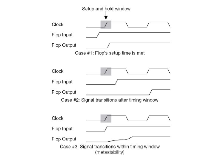
Metastability • Metastability is a phenomenon that may occur if the setup and hold time requirements of the FF are not met, leading in the output settling in an unknown value after unspecified time.
Reliable synchronizer design
Example • Design a synchronizer that synchronizes two inputs async 1 and async 2 generated with a 50 MHz clock CLK 1, to a system with a 33 MHz clock CLK 2 totally independent of CLK 1. Draw appropriate timing diagrams.
Mean-time between failures f: frequency of flip-flop clock a: number of asynchronous input changes per second in flipflop input To, τ: constants depending on flip-flop electrical characteristics Assume a 10 Mhz clock, ts = 20 ns, To = 0. 4 sec, τ = 1. 5 ns and that the asynchronous input can change 100, 000 times per second, then tr = 1/f – ts = 80 ns MTBF(80 ns) = exp(80/1. 5)/0. 4× 10^7× 10^5= 3. 6× 10^11 s
Cascaded synchronizer
Synchronizing bus transfers • Do not use dual f/f synchronizers in all bits, this will only increase the chances of metastability • Synchronize the control signals and read the input when safe to do so
Synchronization circuit
Synchronizing high-speed data transfers • What happens when the asynchronous inputs are clocked faster than the system clock? Or in a long burst transfer such as AXI bus?
FIFO Synchronizer basic concept • On burst transfers, the receiver cannot afford to wait for the signal to settle. • Solution: A dual-port RAM FIFO • Problem: How do we synchronize the counters?
Summary • In order to avoid hazards and races, synchronous design is used • In synchronous design a single common clock is used and reset is only used for initialization • The only considerations in synchronous design are the flip-flop setup and hold times, clock skew and asynchronous input synchronization • Asynchronous inputs are commonly synchronized using 2 flip-flops clocked with the synchronous system clock • Synchronization should only be done in one place • In bus transfers, synchronize only the control signals or use a FIFO