Surface Preparation and Wet Processing Thomas S Roche


- Slides: 47

Surface Preparation and Wet Processing Thomas S. Roche, Ph. D. Motorola Corporation 1999 Arizona Board of Regents for The University of Arizona NSF/SRC Engineering Research Center for Environmentally Benign Semiconductor Manufacturing 1

Outline • Why wet processing? – Etching and cleaning • What chemicals are used? – Chemistry of the processes NSF/SRC Engineering Research Center for Environmentally Benign Semiconductor Manufacturing 2

Why Wet Processing? • Isotropic • Non-damaging • Selective • Clean - particle and metal contaminant removal • Well understood NSF/SRC Engineering Research Center for Environmentally Benign Semiconductor Manufacturing 3

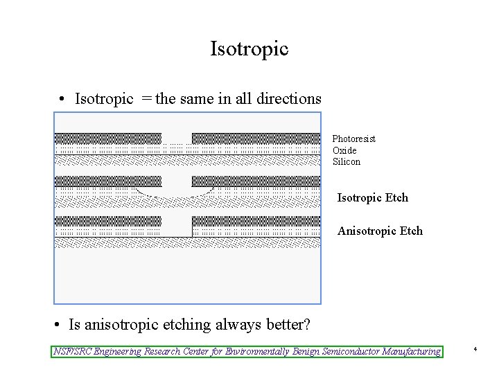
Isotropic • Isotropic = the same in all directions Photoresist Oxide Silicon Isotropic Etch Anisotropic Etch • Is anisotropic etching always better? NSF/SRC Engineering Research Center for Environmentally Benign Semiconductor Manufacturing 4

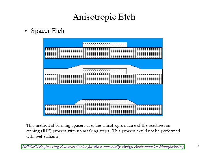
Anisotropic Etch • Spacer Etch This method of forming spacers uses the anisotropic nature of the reactive ion etching (RIE) process with no masking steps. This process could not be performed with wet etchants. NSF/SRC Engineering Research Center for Environmentally Benign Semiconductor Manufacturing 5

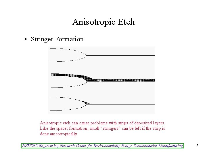
Anisotropic Etch • Stringer Formation Anisotropic etch can cause problems with strips of deposited layers. Like the spacer formation, small “stringers” can be left if the strip is done anisotropically. NSF/SRC Engineering Research Center for Environmentally Benign Semiconductor Manufacturing 6

Non-Damaging • Reactive ion etching and plasma etching can damage silicon surfaces. – These techniques also have some etching effect on the silicon surface. • HF solutions show better selectivity of oxide to silicon than plasma. – An HF solution has fewer chemical species than a fluorine based plasma. It is a better controlled reactant than a plasma. NSF/SRC Engineering Research Center for Environmentally Benign Semiconductor Manufacturing 7

Wet Etch Solutions • HF and Buffered Oxide Etchant - oxide etch • Phosphoric Acid - nitride etch • Nitric Acid and HF - polysilicon etch • Selective metal etches – Al etch - nitric acid, phosphoric acid, acetic acid Ti etch - ammonium hydroxide and hydrogen peroxide W etch - hydrogen peroxide and ammonium hydroxide • Potassium hydroxide solution - silicon etch NSF/SRC Engineering Research Center for Environmentally Benign Semiconductor Manufacturing 8

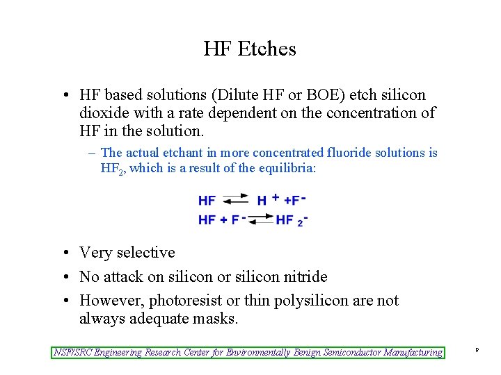
HF Etches • HF based solutions (Dilute HF or BOE) etch silicon dioxide with a rate dependent on the concentration of HF in the solution. – The actual etchant in more concentrated fluoride solutions is HF 2, which is a result of the equilibria: • Very selective • No attack on silicon or silicon nitride • However, photoresist or thin polysilicon are not always adequate masks. NSF/SRC Engineering Research Center for Environmentally Benign Semiconductor Manufacturing 9

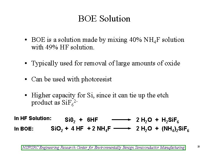
BOE Solution • BOE is a solution made by mixing 40% NH 4 F solution with 49% HF solution. • Typically used for removal of large amounts of oxide • Can be used with photoresist • Higher capacity for Si, since it can tie up the etch product as Si. F 62 In HF Solution: In BOE: Si 02 + 6 HF Si. O 2 + 4 HF + 2 NH 4 F 2 H 2 O + H 2 Si. F 6 2 H 2 O + (NH 4)2 Si. F 6 NSF/SRC Engineering Research Center for Environmentally Benign Semiconductor Manufacturing 10

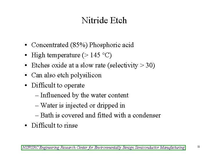
Nitride Etch • • • Concentrated (85%) Phosphoric acid High temperature (> 145 °C) Etches oxide at a slow rate (selectivity > 30) Can also etch polysilicon Difficult to operate – Influenced by the water content – Water is injected or dripped in – Bath is covered and fitted with a condenser • Difficult to rinse NSF/SRC Engineering Research Center for Environmentally Benign Semiconductor Manufacturing 11

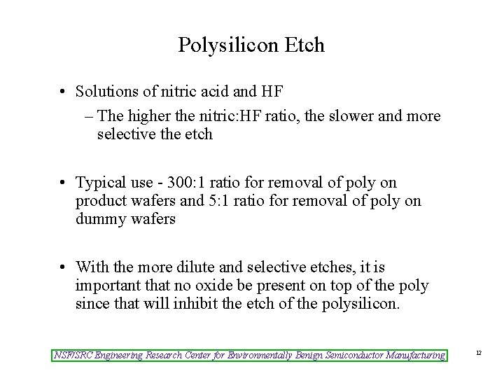
Polysilicon Etch • Solutions of nitric acid and HF – The higher the nitric: HF ratio, the slower and more selective the etch • Typical use - 300: 1 ratio for removal of poly on product wafers and 5: 1 ratio for removal of poly on dummy wafers • With the more dilute and selective etches, it is important that no oxide be present on top of the poly since that will inhibit the etch of the polysilicon. NSF/SRC Engineering Research Center for Environmentally Benign Semiconductor Manufacturing 12

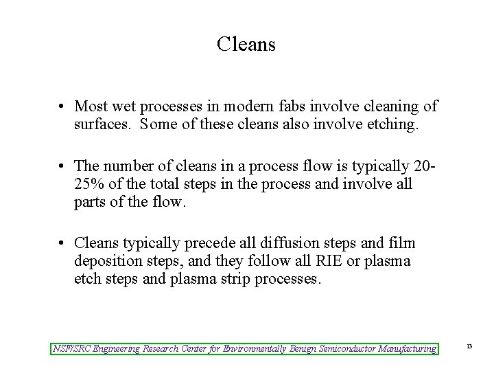
Cleans • Most wet processes in modern fabs involve cleaning of surfaces. Some of these cleans also involve etching. • The number of cleans in a process flow is typically 2025% of the total steps in the process and involve all parts of the flow. • Cleans typically precede all diffusion steps and film deposition steps, and they follow all RIE or plasma etch steps and plasma strip processes. NSF/SRC Engineering Research Center for Environmentally Benign Semiconductor Manufacturing 13

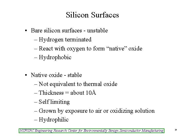
Silicon Surfaces • Bare silicon surfaces - unstable – Hydrogen terminated – React with oxygen to form “native” oxide – Hydrophobic • Native oxide - stable – Not equivalent to thermal oxide – Thickness = about 10Å – Self limiting – Grown by exposure to air or oxidizing solution – Hydrophilic NSF/SRC Engineering Research Center for Environmentally Benign Semiconductor Manufacturing 14

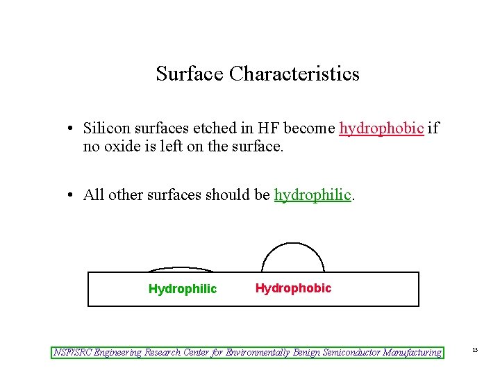
Surface Characteristics • Silicon surfaces etched in HF become hydrophobic if no oxide is left on the surface. • All other surfaces should be hydrophilic. Hydrophilic Hydrophobic NSF/SRC Engineering Research Center for Environmentally Benign Semiconductor Manufacturing 15

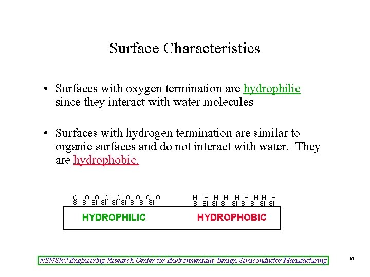
Surface Characteristics • Surfaces with oxygen termination are hydrophilic since they interact with water molecules • Surfaces with hydrogen termination are similar to organic surfaces and do not interact with water. They are hydrophobic. O O O O O SI SI SI HYDROPHILIC H H H H H SI SI SI HYDROPHOBIC NSF/SRC Engineering Research Center for Environmentally Benign Semiconductor Manufacturing 16

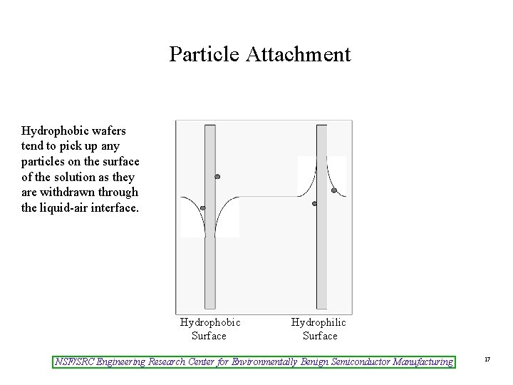
Particle Attachment Hydrophobic wafers tend to pick up any particles on the surface of the solution as they are withdrawn through the liquid-air interface. Hydrophobic Surface Hydrophilic Surface NSF/SRC Engineering Research Center for Environmentally Benign Semiconductor Manufacturing 17

Oxide Surfaces • Oxide surfaces can be formed: – by room temperature oxidation of “bare” silicon surfaces (native oxide) – by heating silicon in an oxygen atmosphere (thermal oxide) – by deposition in a low pressure furnace (LPCVD oxide) – by deposition from decomposition of TEOS in a plasma reactor (plasma TEOS or plasma oxide) • All oxide surfaces are hydrophilic, but they etch at different rates in HF. NSF/SRC Engineering Research Center for Environmentally Benign Semiconductor Manufacturing 18

Cleaning Solutions • Sulfuric Acid-Hydrogen Peroxide (aka SPM or Piranha) solution Ù Organic removal • Ammonium Hydroxide-Hydrogen Peroxide (aka SC 1 or APM) Ù Particle removal • Hydrochloric Acid-Hydrogen Peroxide (aka SC 2 or HPM) Ù Metallic contamination removal • Dilute HF solutions Ù Metallic contamination removal with oxide removal NSF/SRC Engineering Research Center for Environmentally Benign Semiconductor Manufacturing 19

Sulfuric Acid-Hydrogen Peroxide (SPM/Piranha) • Operated at > 100°C • Useful for its oxidizing (organic destruction) capabilities • Will grow an oxide on bare silicon but will not grow oxide on oxidized surfaces • Peroxide has a limited lifetime, replenished by spiking with added peroxide NSF/SRC Engineering Research Center for Environmentally Benign Semiconductor Manufacturing 20

Sulfuric Acid-Hydrogen Peroxide (cont’d) • Sulfuric acid disadvantages – Difficult to remove from surfaces – Water used for rinsing is usually very hot • Amount of sulfur left on surfaces is very high. – Removed easily with a brief HF dip • Solutions also effective in removal of some metal contamination NSF/SRC Engineering Research Center for Environmentally Benign Semiconductor Manufacturing 21

Sulfuric Acid-Ozone • Some facilities use sulfuric acid with ozone bubbled through it • Effective solution – Long bath life - no water added – Easily overwhelmed by organics • Another variant - ozone in cold water – Good oxidant – Rate of resist removal is fairly slow NSF/SRC Engineering Research Center for Environmentally Benign Semiconductor Manufacturing 22

NH 4 OH-H 2 O 2 (SC 1/APM) • Typically used with a Megasonic unit for particle removal • Temperature range of 50 -80°C • Standard solution is 5: 1: 1 of water: ammonia: peroxide • Problems – Peroxide is unstable in basic solution, especially in the presence of metallic impurities. – Ammonia has high volatility. – Metallic impurities readily adsorb onto surfaces. – Presence of the oxidant is critical! » If lost, solution will etch silicon » Maintained by spiking NSF/SRC Engineering Research Center for Environmentally Benign Semiconductor Manufacturing 23

NH 4 OH-H 2 O 2 Details • Can grow a native (chemical) oxide on a bare silicon – Also etches oxides at a low rate (~1Å/min), therefore can etch silicon • Dilutions down to 50: 1: 1 probably as effective – May have problems the current solutions do not • Al and Fe contamination - typical problem – Other transition metals can also deposit – Can also result in surface roughening NSF/SRC Engineering Research Center for Environmentally Benign Semiconductor Manufacturing 24

NH 4 OH-H 2 O 2 Details (cont’d) • Lower concentrations – More likely to deposit metals – Control of the concentration is critical • Tradeoffs to be considered with lower concentrations: – higher changeout frequency/shorter bath life – lower particle removal efficiency – metallic contamination – ammonia evaporation and peroxide decomposition NSF/SRC Engineering Research Center for Environmentally Benign Semiconductor Manufacturing 25

HCl-H 2 O 2 (SC 2/HPM) • Temperature range of 50 -70°C • Standard dilution is 5: 1: 1 of water: HCl: peroxide • Mechanism for operation - chlorides of most metallic contaminants are soluble in an acidic solution • Peroxide may not be needed at low metallic contamination levels. NSF/SRC Engineering Research Center for Environmentally Benign Semiconductor Manufacturing 26

Solvent Based Cleaning Solutions • Resist strippers - proprietary mixtures of organic solvents and active ingredients – – The solvents are typically NMP (N-methyl pyrrolidone) NMP is water soluble and neutral in aqueous solution “Active ingredients” are typically amines Attack the resist and dissolve into the solvent media. • New strippers - “semi-aqueous”, containing both organic solvents and water along with “active ingredients” and corrosion inhibitors NSF/SRC Engineering Research Center for Environmentally Benign Semiconductor Manufacturing 27

Solvent Based Cleaning Solutions: Problems • Corrosion of metal lines due to the transition of the surface from the organic solution to rinse water • Any “active ingredients” left on the surface attack the metal in water – Solution- use an intermediate rinse solvent • Metallic contamination (especially sodium) – Solution - use only low sodium strippers – Less of a problem with “semi-aqueous” strippers NSF/SRC Engineering Research Center for Environmentally Benign Semiconductor Manufacturing 28

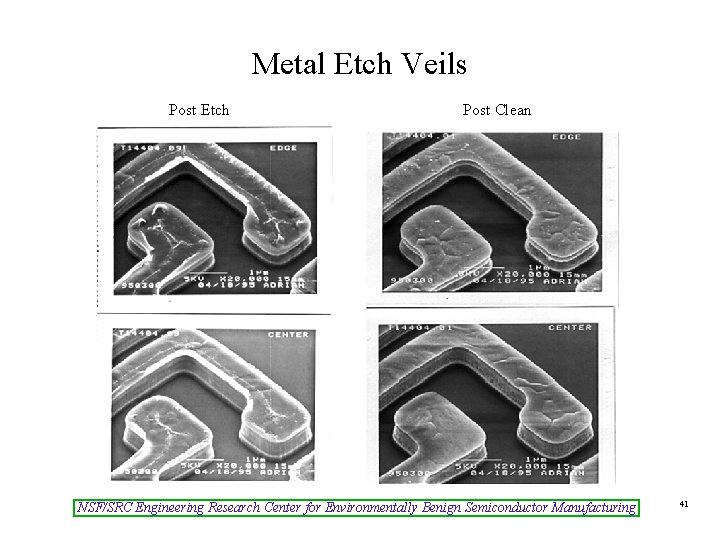
Solvent Modified Cleans e. g. EG-BOE • Residues after metal etch processes often contain compounds of the metal etched, along with other species. • Cleaners contain fluoride and a polar solvent such as ethylene glycol to dissolve these metallic compounds. • Involves a balance of acidity and etching of the fluoride with the inhibition of metal attack by ethylene glycol NSF/SRC Engineering Research Center for Environmentally Benign Semiconductor Manufacturing 29

Water • Most heavily used chemical - 2000 gal/wafer • Used mainly for removing other chemicals • Rinse times – until solution reaches high resistivity – given time period • Problems – Bacteria – TOC – Metallic contamination NSF/SRC Engineering Research Center for Environmentally Benign Semiconductor Manufacturing 30

Wafer Rinsing • Continuous flow of water past wafers • Completion of rinse is determined by measuring the resistivity of the water (Resistivity = very sensitive method of determining the presence of ions in solution) • Dump rinsing - used for wafers that are hydrophilic • Hot water - used after some processes (but not HF treated surfaces) NSF/SRC Engineering Research Center for Environmentally Benign Semiconductor Manufacturing 31

Wafer Rinsing, cont’d • Resistivity measurements describe the purity of the water in the rinse bath - not the amount of chemical left on the wafer. NSF/SRC Engineering Research Center for Environmentally Benign Semiconductor Manufacturing 32

Bacterial Contamination • All DI systems contain bacteria, which can grow and contaminate systems if nutrients are provided. • Ozonation or hydrogen peroxide (oxidizing agent) is typically employed to keep down bacterial levels. • Once bacterial contamination is established, it is difficult to remove since the bacteria form colonies which are difficult to completely destroy with oxidant solutions. NSF/SRC Engineering Research Center for Environmentally Benign Semiconductor Manufacturing 33

Drying • Critical step in cleaning • Objective - remove as much of the water as possible before it can dry on the surface and leave residues from any impurities in the water • Two types of dryers – Spin rinse dryer (SRD) - throw off as much water as possible – IPA vapor - displace water with IPA » IPA vapor dryer styles • Tank • Vapor jet (VJD) • Marangoni-type NSF/SRC Engineering Research Center for Environmentally Benign Semiconductor Manufacturing 34

IPA “Vapor Jet” Dryer NSF/SRC Engineering Research Center for Environmentally Benign Semiconductor Manufacturing 35

Marangoni Drying A low concentration of IPA vapor condenses on the water surface. As the wafers are withdrawn slowly from the water, the IPA layer displaces the water. The IPA evaporates from the wafers and they are dried. NSF/SRC Engineering Research Center for Environmentally Benign Semiconductor Manufacturing 36

Types of Cleans • Resist Strips - post etch and post implant • Etch residue removal • Pre-Metal deposition cleans • Pre-diffusion cleans NSF/SRC Engineering Research Center for Environmentally Benign Semiconductor Manufacturing 37

Resist Strip • Resist removed by ashing - a plasma process which “burns” the resist off the surface (Note - Resist contains measurable amounts of impurities such as sodium. ) • Ashing concentrates impurities on the surface. – Must be followed by a wet process to remove contaminants • Sulfuric acid-hydrogen peroxide used before metal is present on the wafer • Solvent strippers used after metal deposition NSF/SRC Engineering Research Center for Environmentally Benign Semiconductor Manufacturing 38

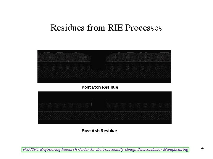
Post-Etch Cleans • Reactive ion etching (RIE) = a physical-chemical process which can leave residues • Difficult to remove (can be fluorinated polymers) so both ash and wet clean are usually used – Residues are created to inhibit attack of the plasma on the sidewall of the etched film – Changes in the etch process or the material being etched can require changes in the clean NSF/SRC Engineering Research Center for Environmentally Benign Semiconductor Manufacturing 39

Residues from RIE Processes Post Etch Residue Post Ash Residue NSF/SRC Engineering Research Center for Environmentally Benign Semiconductor Manufacturing 40

Metal Etch Veils Post Etch Post Clean NSF/SRC Engineering Research Center for Environmentally Benign Semiconductor Manufacturing 41

Post Implant Resist Strip • Implantation sometimes uses resist masks • High dose implants can convert photoresist to a coaltype material – Can be ashed if it is done carefully, but problems can result • Residue can be more complex since it can contain residue from the implant • May require more than a sulfuric-peroxide clean NSF/SRC Engineering Research Center for Environmentally Benign Semiconductor Manufacturing 42

Pre-Metal Contact Clean • Clean before metal is deposited • Connects the silicon circuit to the metal lines on top of the die • Nature of the silicon surface is critical to the metal contact resistance • Performed with HF containing etchant – Important consideration - selectivity of the etchant to the films present (e. g. oxide, BPSG, TEOS) NSF/SRC Engineering Research Center for Environmentally Benign Semiconductor Manufacturing 43

Metal Contact NSF/SRC Engineering Research Center for Environmentally Benign Semiconductor Manufacturing 44

Pre-Diffusion Clean • Cleans before furnace operations are critical – Defects or contamination will be incorporated into the wafer if not removed prior to furnace • Most important steps - those where bare silicon is present – Pre-initial – Pre-sac gate – Pre-gate • Typically full cleans (Piranha+BOE+SC 1+SC 2) NSF/SRC Engineering Research Center for Environmentally Benign Semiconductor Manufacturing 45

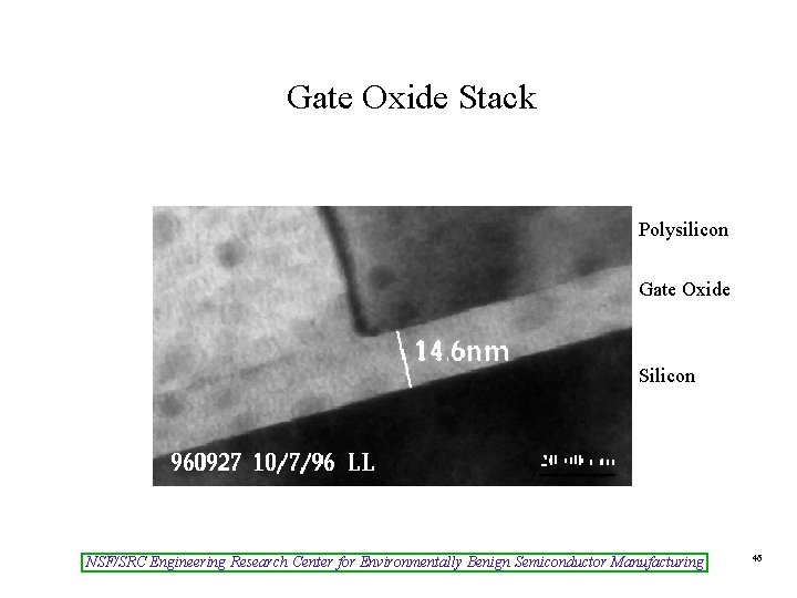
Gate Oxide Stack Polysilicon Gate Oxide Silicon NSF/SRC Engineering Research Center for Environmentally Benign Semiconductor Manufacturing 46

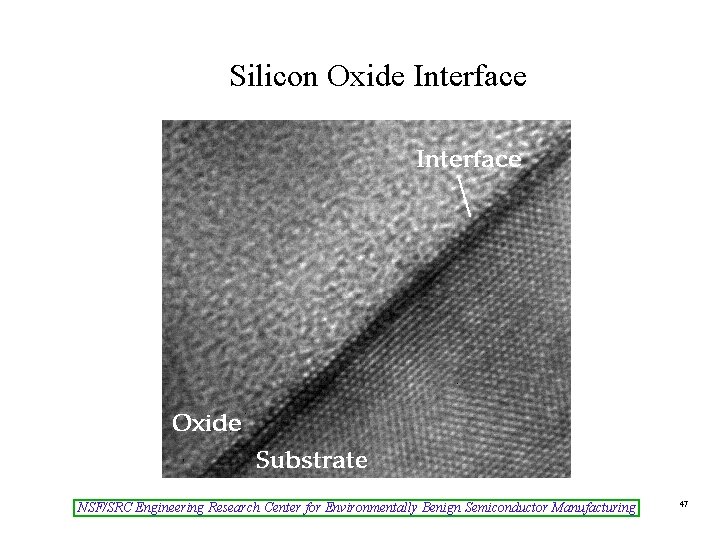
Silicon Oxide Interface NSF/SRC Engineering Research Center for Environmentally Benign Semiconductor Manufacturing 47