Surface Potential Imaging of Organic Semiconductors by Kelvin

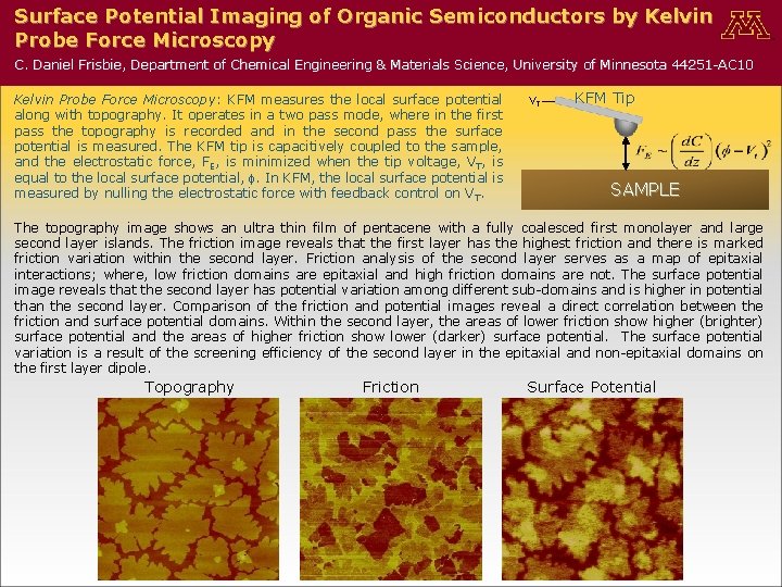
Surface Potential Imaging of Organic Semiconductors by Kelvin Probe Force Microscopy C. Daniel Frisbie, Department of Chemical Engineering & Materials Science, University of Minnesota 44251 -AC 10 Kelvin Probe Force Microscopy: KFM measures the local surface potential along with topography. It operates in a two pass mode, where in the first pass the topography is recorded and in the second pass the surface potential is measured. The KFM tip is capacitively coupled to the sample, and the electrostatic force, FE, is minimized when the tip voltage, VT, is equal to the local surface potential, f. In KFM, the local surface potential is measured by nulling the electrostatic force with feedback control on V T. VT KFM Tip SAMPLE The topography image shows an ultra thin film of pentacene with a fully coalesced first monolayer and large second layer islands. The friction image reveals that the first layer has the highest friction and there is marked friction variation within the second layer. Friction analysis of the second layer serves as a map of epitaxial interactions; where, low friction domains are epitaxial and high friction domains are not. The surface potential image reveals that the second layer has potential variation among different sub-domains and is higher in potential than the second layer. Comparison of the friction and potential images reveal a direct correlation between the friction and surface potential domains. Within the second layer, the areas of lower friction show higher (brighter) surface potential and the areas of higher friction show lower (darker) surface potential. The surface potential variation is a result of the screening efficiency of the second layer in the epitaxial and non-epitaxial domains on the first layer dipole. Topography Friction Surface Potential
- Slides: 1