SURFACE MODIFICATION OF POLYMER PHOTORESISTS TO PROTECT PATTERN
- Slides: 21

SURFACE MODIFICATION OF POLYMER PHOTORESISTS TO PROTECT PATTERN TRANSFER IN FLUOROCARBON PLASMA ETCHING* Mingmei Wanga) and Mark J. Kushnerb) a)Iowa State University, Ames, IA 50011 USA mmwang@iastate. edu b)University of Michigan, Ann Arbor, MI 48109 USA mjkush@umich. edu http: //uigelz. eecs. umich. edu 62 th GEC, October 2009, Saratoga Springs, NY *Work supported by Tokyo Electron Ltd. and Semiconductor Research Corp. MW_GEC 2009

AGENDA · Consequences of ion induced cross-linking on etch rates and photoresist (PR) CD control. · Description of the model · Scaling of mixing and implantation with Ion Energy Distributions · Strategies to control PR erosion · VUV induced degradation and cross-linking of PR · Si extraction (Si. Fx) and deposition on PR and CFx polymer · Concluding Remarks MW_GEC 2009 University of Michigan Institute for Plasma Science & Engr.

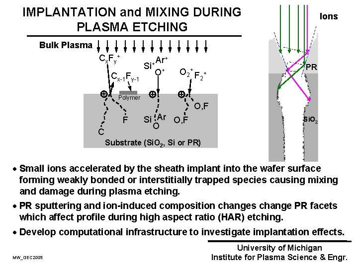
IMPLANTATION and MIXING DURING PLASMA ETCHING Ions Bulk Plasma Cx F y + Cx-1 Fy-1 + Polymer F C Ar+ + Si + O 2 + F 2 + PR + O, F Si Ar O, F O Si. O 2 Substrate (Si. O 2, Si or PR) · Small ions accelerated by the sheath implant into the wafer surface forming weakly bonded or interstitially trapped species causing mixing and damage during plasma etching. · PR sputtering and ion-induced composition changes change PR facets which affect profile during high aspect ratio (HAR) etching. · Develop computational infrastructure to investigate implantation effects. MW_GEC 2009 University of Michigan Institute for Plasma Science & Engr.

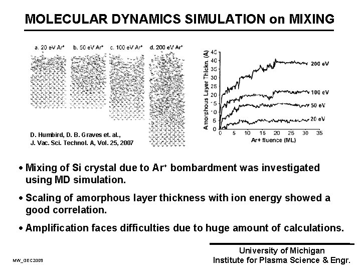
MOLECULAR DYNAMICS SIMULATION on MIXING D. Humbird, D. B. Graves et. al. , J. Vac. Sci. Technol. A, Vol. 25, 2007 · Mixing of Si crystal due to Ar+ bombardment was investigated using MD simulation. · Scaling of amorphous layer thickness with ion energy showed a good correlation. · Amplification faces difficulties due to huge amount of calculations. MW_GEC 2009 University of Michigan Institute for Plasma Science & Engr.

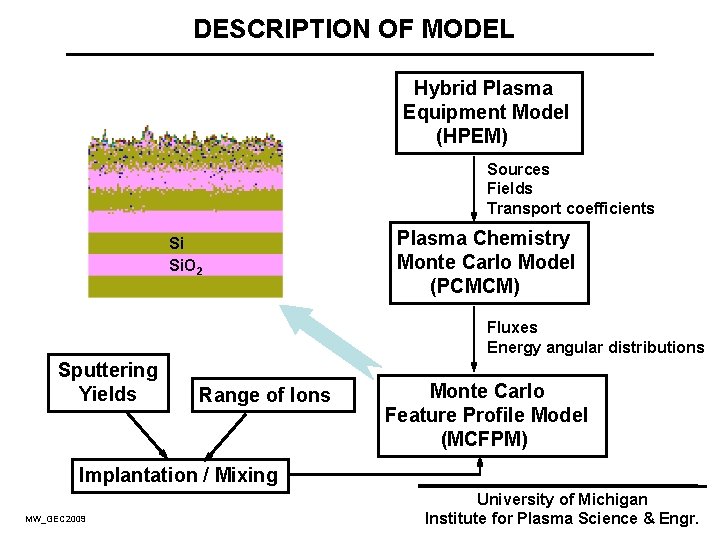
DESCRIPTION OF MODEL Hybrid Plasma Equipment Model (HPEM) Sources Fields Transport coefficients Si Si. O 2 Plasma Chemistry Monte Carlo Model (PCMCM) Fluxes Energy angular distributions Sputtering Yields Range of Ions Monte Carlo Feature Profile Model (MCFPM) Implantation / Mixing MW_GEC 2009 University of Michigan Institute for Plasma Science & Engr.

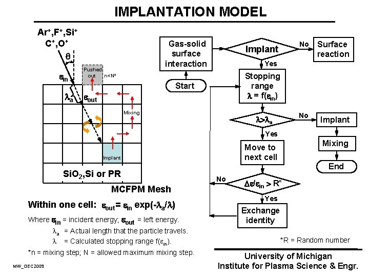
IMPLANTATION MODEL Ar+, F+, Si+ C+, O+ in a Gas-solid surface interaction Pushed out n<N* Implant No Surface reaction No Implant Yes Stopping range = f( in) Start out Mixing a Yes Implant Si. O 2, Si or PR MCFPM Mesh Within one cell: out= in exp(- a/ ) Where in = incident energy; out = left energy. a = Actual length that the particle travels. = Calculated stopping range f( in). *n = mixing step; N = allowed maximum mixing step. MW_GEC 2009 Mixing Move to next cell End No / in R* Yes Exchange identity *R = Random number University of Michigan Institute for Plasma Science & Engr.

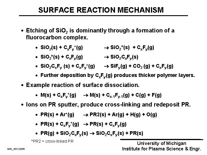
SURFACE REACTION MECHANISM · Etching of Si. O 2 is dominantly through a formation of a fluorocarbon complex. · Si. O 2(s) + Cx. Fy+(g) Si. O 2*(s) + Cx. Fy(g) · Si. O 2*(s) + Cx. Fy(g) Si. O 2 Cx. Fy(s) · Si. O 2 Cx. Fy (s) + Cx. Fy+(g) Si. Fy(g) + CO 2 (g) + Cx. Fy(g) · Further deposition by Cx. Fy(g) produces thicker polymer layers. · Example reaction of surface dissociation. · M(s) + Cx. Fy+(g) M(s) + Cx-1 Fy-1(g) + C(g) + F(g) · Ions on PR sputter, produce cross-linking and redeposit PR. · PR(s) + Ar+(g) PR 2(s) + Ar(g) + H(g) + O(g) · PR(s) + Cx. Fy+(g) PR(s) + Cx. Fy(g) · PR(g) + Si. O 2 Cx. Fy(s) + PR(s) *PR 2 = cross-linked PR MW_GEC 2009 University of Michigan Institute for Plasma Science & Engr.

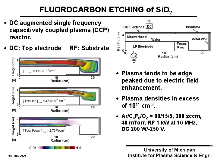
FLUOROCARBON ETCHING of Si. O 2 · DC augmented single frequency capacitively coupled plasma (CCP) reactor. · DC: Top electrode RF: Substrate · Plasma tends to be edge peaked due to electric field enhancement. · Plasma densities in excess of 1011 cm-3. · Ar/C 4 F 8/O 2 = 80/15/5, 300 sccm, 40 m. Torr, RF 1 k. W at 10 MHz, DC 200 W/-250 V. MW_GEC 2009 University of Michigan Institute for Plasma Science & Engr.

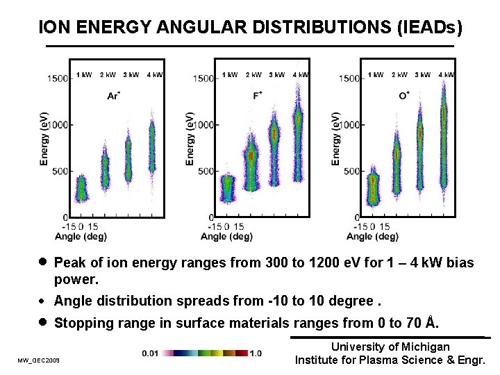
ION ENERGY ANGULAR DISTRIBUTIONS (IEADs) · Peak of ion energy ranges from 300 to 1200 e. V for 1 – 4 k. W bias power. · Angle distribution spreads from -10 to 10 degree. · Stopping range in surface materials ranges from 0 to 70 Å. MW_GEC 2009 University of Michigan Institute for Plasma Science & Engr.

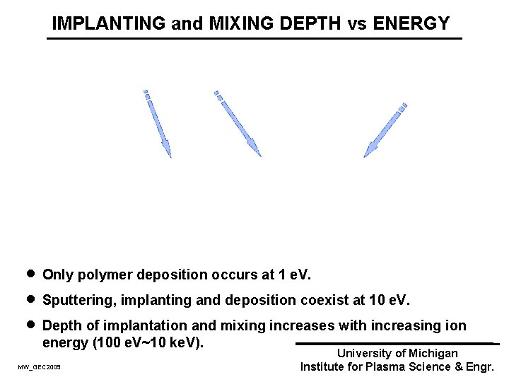
IMPLANTING and MIXING DEPTH vs ENERGY · Only polymer deposition occurs at 1 e. V. · Sputtering, implanting and deposition coexist at 10 e. V. · Depth of implantation and mixing increases with increasing ion energy (100 e. V~10 ke. V). MW_GEC 2009 University of Michigan Institute for Plasma Science & Engr.

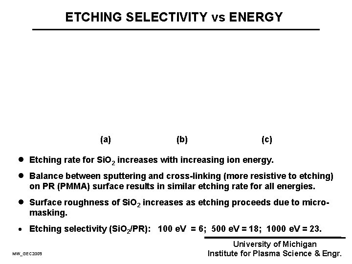
ETCHING SELECTIVITY vs ENERGY (a) · · · (b) (c) Etching rate for Si. O 2 increases with increasing ion energy. Balance between sputtering and cross-linking (more resistive to etching) on PR (PMMA) surface results in similar etching rate for all energies. Surface roughness of Si. O 2 increases as etching proceeds due to micromasking. · Etching selectivity (Si. O 2/PR): 100 e. V = 6; 500 e. V = 18; 1000 e. V = 23. MW_GEC 2009 University of Michigan Institute for Plasma Science & Engr.

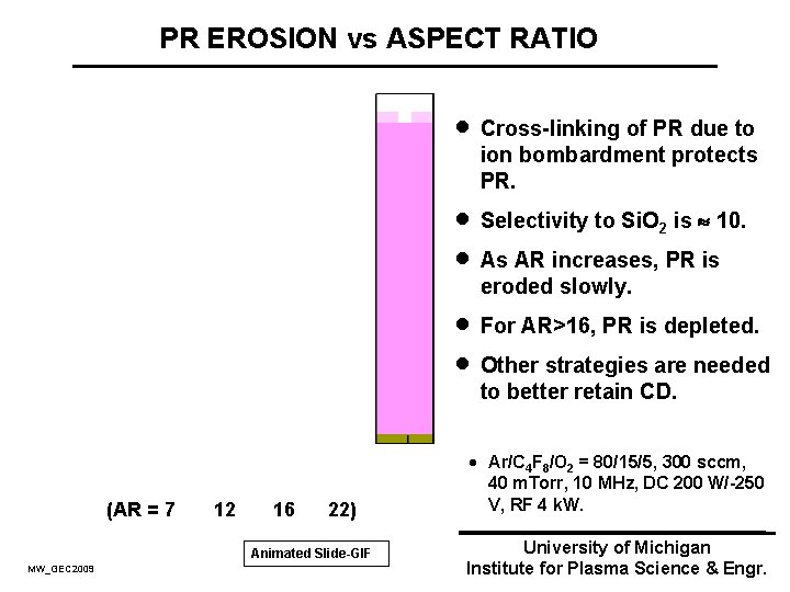
PR EROSION vs ASPECT RATIO · Cross-linking of PR due to ion bombardment protects PR. · Selectivity to Si. O 2 is 10. · As AR increases, PR is eroded slowly. · For AR>16, PR is depleted. · Other strategies are needed to better retain CD. (AR = 7 12 16 22) Animated Slide-GIF MW_GEC 2009 · Ar/C 4 F 8/O 2 = 80/15/5, 300 sccm, 40 m. Torr, 10 MHz, DC 200 W/-250 V, RF 4 k. W. University of Michigan Institute for Plasma Science & Engr.

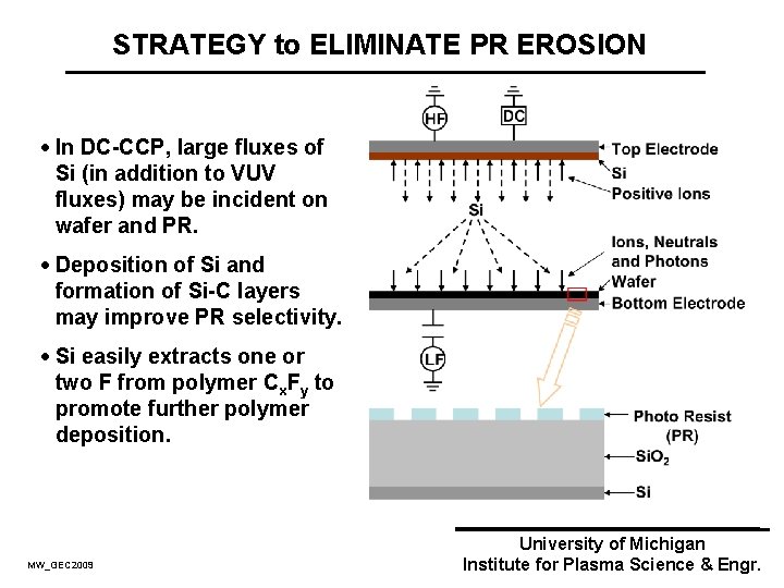
STRATEGY to ELIMINATE PR EROSION · In DC-CCP, large fluxes of Si (in addition to VUV fluxes) may be incident on wafer and PR. · Deposition of Si and formation of Si-C layers may improve PR selectivity. · Si easily extracts one or two F from polymer Cx. Fy to promote further polymer deposition. MW_GEC 2009 University of Michigan Institute for Plasma Science & Engr.

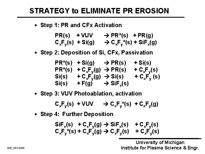
STRATEGY to ELIMINATE PR EROSION · Step 1: PR and CFx Activation PR(s) + VUV Cx. Fy(s) + Si(g) PR*(s) + PR(g) Cx. Fy*(s) + Si. Fx(g) · Step 2: Deposition of Si, CFx, Passivation PR*(s) Si(s) + Si(g) + Cx. Fy(g) + F(g) PR(s) + Si(s) PR(s) + Cx. Fy(s) Si(s) + Cx. Fy (s) Si. Fx(s) · Step 3: VUV Photoablation, activation Cx. Fy(s) + VUV Cx. Fy*(s) + Cx. Fy(g) · Step 4: Further Deposition Si. Fx(s) + Cx. Fy(g) Si. Fx(s) + Cx. Fy(s) Cx. Fy*(s) + Cx. Fy(g) Cx. Fy(s) + Cx. Fy(s) MW_GEC 2009 University of Michigan Institute for Plasma Science & Engr.

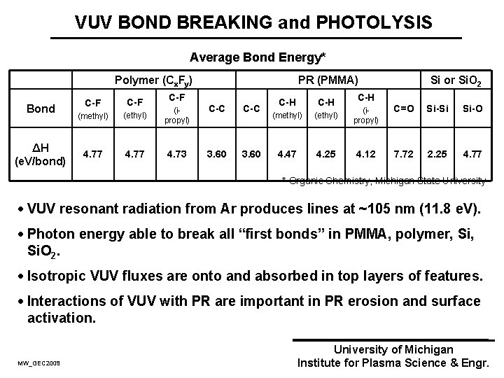
VUV BOND BREAKING and PHOTOLYSIS Average Bond Energy* Polymer (Cx. Fy) Bond ΔH (e. V/bond) PR (PMMA) C-F C-F (methyl) (ipropyl) C-C 4. 77 4. 73 3. 60 Si or Si. O 2 C-H C-H (methyl) (ipropyl) C=O Si-Si Si-O 4. 47 4. 25 4. 12 7. 72 2. 25 4. 77 * Organic Chemistry, Michigan State University · VUV resonant radiation from Ar produces lines at ~105 nm (11. 8 e. V). · Photon energy able to break all “first bonds” in PMMA, polymer, Si. O 2. · Isotropic VUV fluxes are onto and absorbed in top layers of features. · Interactions of VUV with PR are important in PR erosion and surface activation. MW_GEC 2009 University of Michigan Institute for Plasma Science & Engr.

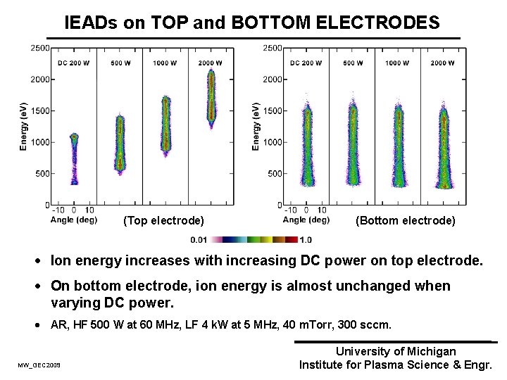
IEADs on TOP and BOTTOM ELECTRODES (Top electrode) (Bottom electrode) · Ion energy increases with increasing DC power on top electrode. · On bottom electrode, ion energy is almost unchanged when varying DC power. · AR, HF 500 W at 60 MHz, LF 4 k. W at 5 MHz, 40 m. Torr, 300 sccm. MW_GEC 2009 University of Michigan Institute for Plasma Science & Engr.

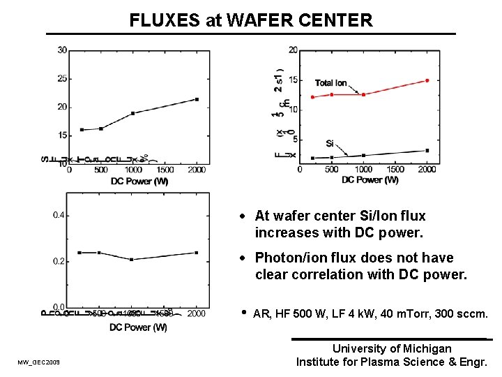
FLUXES at WAFER CENTER · At wafer center Si/Ion flux increases with DC power. · Photon/ion flux does not have clear correlation with DC power. • MW_GEC 2009 AR, HF 500 W, LF 4 k. W, 40 m. Torr, 300 sccm. University of Michigan Institute for Plasma Science & Engr.

PROTECTING PR WITH VUV and Si FLUXES · Without Si and VUV exposure, PR is slowly etched (~8 nm/min). · Cross linking by VUV flux has a small effect. · Si flux ultimately increases polymer deposition and Si-C rich layer. · Combination of VUV and Si induces more polymer deposition. • Ar/C 4 F 8/O 2=80/15/5, HF 500 W, LF 4 k. W, DC 2 k. W, 40 m. Torr, 300 sccm. MW_GEC 2009 University of Michigan Institute for Plasma Science & Engr.

VUV FLUX vs PR ETCHING · Increasing VUV flux induces more cross-linking and activated surface sites. · Cross-linked PR is more resistive to etch. · With highly cross-linked PR at high VUV flux, polymer deposition dominates. • Ar/C 4 F 8/O 2=80/15/5, HF 500 W, LF 4 k. W, DC 2 k. W, 40 m. Torr, 300 sccm. MW_GEC 2009 University of Michigan Institute for Plasma Science & Engr.

Si FLUX vs PR ETCHING · Si deposition and its promotion of polymer deposition protects PR from sputtering and erosion. · Sensitivity of balance of PR etching and deposition with respect to Si flux is being investigated. • Ar/C 4 F 8/O 2=80/15/5, HF 500 W, LF 4 k. W, DC 2 k. W, 40 m. Torr, 300 sccm. MW_GEC 2009 University of Michigan Institute for Plasma Science & Engr.

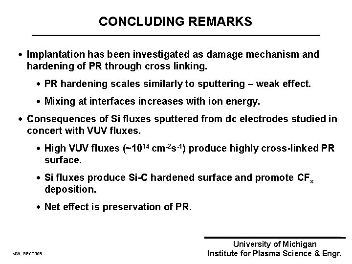
CONCLUDING REMARKS · Implantation has been investigated as damage mechanism and hardening of PR through cross linking. · PR hardening scales similarly to sputtering – weak effect. · Mixing at interfaces increases with ion energy. · Consequences of Si fluxes sputtered from dc electrodes studied in concert with VUV fluxes. · High VUV fluxes (~1014 cm-2 s-1) produce highly cross-linked PR surface. · Si fluxes produce Si-C hardened surface and promote CFx deposition. · Net effect is preservation of PR. MW_GEC 2009 University of Michigan Institute for Plasma Science & Engr.