Summary of Introduction MEMS U S Sometimes Microsystems
 Sometimes Microsystems in Europe. • MEMS=Micro.")


, Campbell or other IC fabrication text (generally good, but incomplete for")


")

 • Metals (~Solders, Metal/Semiconductor Eutectics)")


- Slides: 64
Summary of Introduction • MEMS (U. S. ) Sometimes Microsystems in Europe. • MEMS=Micro. Electro. Mechanical Systems • Very broad definition in practice: Mechanical, Electrical, Optical, Thermal, Fluidic, Chemical, Magnetic. • Generally systems created using microfabrication that are not integrated circuits. Many (but not all) of the microfabrication techniques were borrowed from the IC industry. • Market is smaller than IC market, but more diverse and growing faster.
Some Examples • Accelerometer – Electrical/Mechanical • m. TAS or Micro Total Analysis System – Purifies, amplifies, and detects DNA, for example. – Fluids/Biochemistry/Optical/Electrical • TI DLP – Optical/Mechanical/Electrical/Surface Science • Microrelay – Mechanical/Electrical/Surface Science • Microplasma Source – Electrical/Electromagnetic/Plasma • What do you need to know for MEMS? • Everything!!!? ? ? • Truly an interdisciplinary field.
What are we going to do? • Learn a useful subset of techniques needed for designing MEMS devices. Not all!! • We will design MEMS devices. – Project teaming survey is due Monday – see web site. – Project assignment to be posted on the web site. • We will discuss examples of MEMS devices and use the techniques we have developed. • First we will look at microfabrication and process integration. • Other notes: – First homework is due Thursday. We will try to have all students consolidated to one section to make the discussion board and the electronic turn-in (for video streaming students) in one place by Thursday. – Second homework is due Thursday, Sept. 23 (but you will have everything you need to do the work over the weekend). Homework 3 will probably be due on Monday, Sept. 27. The homework load will decrease as the project load increases (generally).
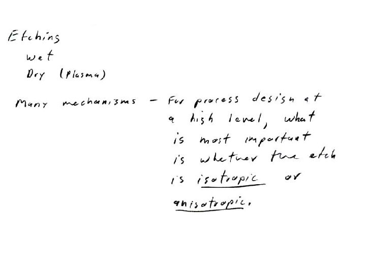
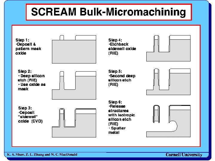
Microfabrication: Types of Micromachining for MEMS • Bulk Micromachining – Etch away large parts of the silicon wafer. – Traditionally, KOH or other chemical etch. – Recently DRIE (Deep Reactive Ion Etch), an anisotropic plasma etch.
Microfabrication: Types of Micromachining for MEMS • Surface micromachining – On surface of wafer/substrate – Sometimes can be a post-process on top of CMOS wafer for process integration with electronics. – Typically much thinner structures than bulk micromachining, but metal structures can be fairly thick.
Microfabrication: Types of Micromachining for MEMS • LIGA – X-ray lithographie, galvanoformung, abformtechnik (or lithography, electrodeposition, and molding). – A special type of surface micromachining, not much used in its original form. – Now sometimes refers to using very thick photoresist to make thick electroplated structures.
Packaging • Ideally, part of fabrication process, then just use a cheap plastic package. • Often, a surface micromachined device is bonded to a bulk micromachined package (the cavity to contain the device is etched from the wafer using bulk micromachining). • Sometimes the package is the most expensive part of the device (pressure sensors, microfluidics). Especially true when the device interacts with the outside environment.
References: Text (brief), Campbell or other IC fabrication text (generally good, but incomplete for MEMS), Madou (specific to MEMS).
Silicon wafer fabrication • Taken from www. egg. or. jp/MSIL/english/index-e. html
Silicon wafer fabrication – slicing and polishing • Taken from www. egg. or. jp/MSIL/english/index-e. html
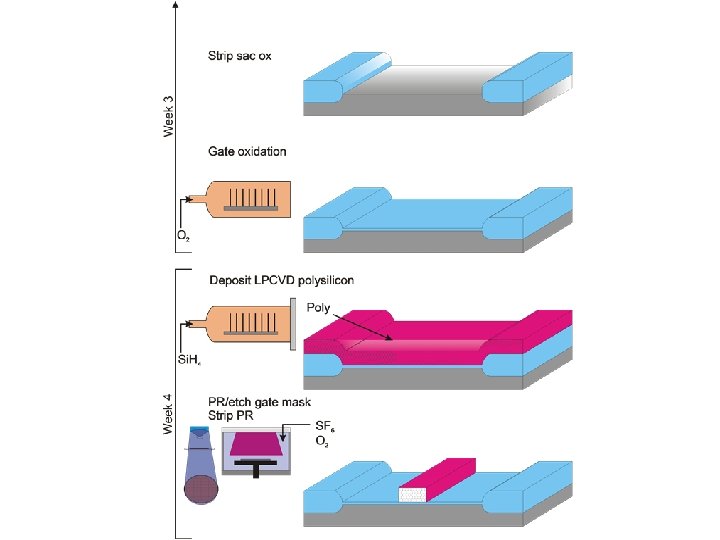
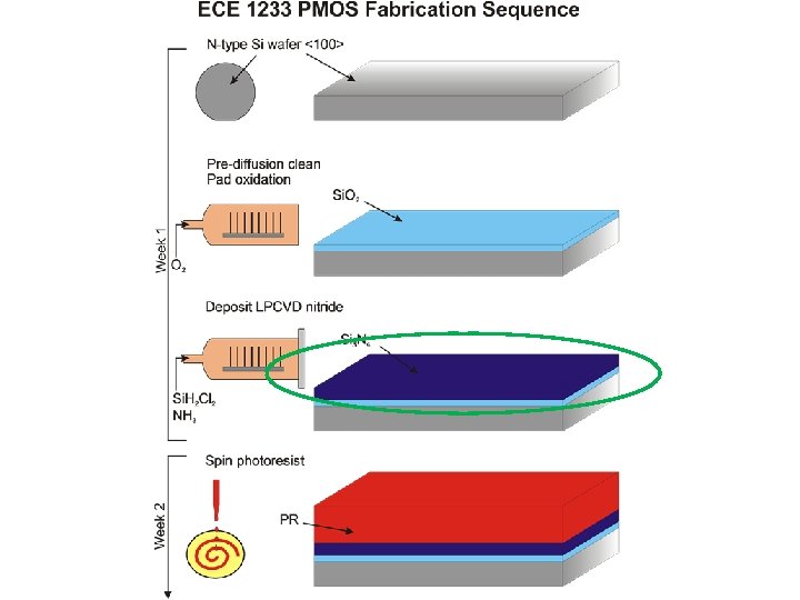
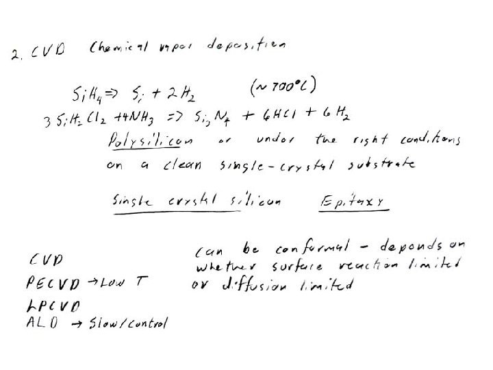
LPCVD Systems Taken from http: //www-bsac. EECS. Berkeley. EDU/~pister/245/
Electrodeposition/Electroplating Surface Micromachined Post-Process Integration with CMOS 20 -100 V Electrostatic Actuation ~100 Micron Size Gate Drain Beam Drain Gate Source Gate Drain SEM of NEU microswitch Source
IBM 7 -Level Cu Metallization (Electroplated)
Packaging • Ideally, part of fabrication process, then just use a cheap plastic package. • Often, a surface micromachined device is bonded to a bulk micromachined package (the cavity to contain the device is etched from the wafer using bulk micromachining). • Sometimes the package is the most expensive part of the device (pressure sensors, microfluidics). Especially true when the device interacts with the outside environment.
• Adhesives • Organics • Glass (Glass Frit) • Metals (~Solders, Metal/Semiconductor Eutectics) • Thermal Compression Bonding • Au-Au/Clean/300 C • Why?
NUMEM Microrelay Process
NUMEM Microrelay Process
Residual stress gradients Taken from http: //www-bsac. EECS. Berkeley. EDU/~pister/245/ More tensile on top More compressive on top Just right! The bottom line: anneal poly between oxides with similar phosphorous content. ~1000 C for ~60 seconds is enough.
Residual stress gradients Taken from http: //www-bsac. EECS. Berkeley. EDU/~pister/245/ A bad day at MCNC (1996).
DRIE structures Taken from http: //www-bsac. EECS. Berkeley. EDU/~pister/245/ • Increased capacitance for actuation and sensing • Low-stress structures – single-crystal Si only structural material Thermal Actuator Comb-drive Actuator • Highly stiff in vertical direction – isolation of motion to wafer plane – flat, robust structures 2 Do. F Electrostatic actuator
Scalloping and Footing issues of DRIE <100 nm silicon nanowire over >10 micron gap 1 µm microgrid Footing at the bottom of Milanovic et al, IEEE TED, Jan. 2001. device layer
Taken from: http: //www. imm-mainz. de/english/sk_a_tec/basic_te/liga. html
Sub-Micron Stereo Lithography New Micro Stereo Lithography for Freely Movable 3 D Micro Structure -Super IH Process with Submicron Resolution. Koji Ikuta, Shoji Maruo, and Syunsuke Kojima Department of Micro System Engineering, school of Engineering, Nagoya University Furocho, Chikusa-ku, Nagonya 464 -01, Japan Tel: +81 52 789 5024, Fax: +81 52 789 5027 E-mail: ikuta@mech. nagoya-u. ac. jp Fig. 6 Schematic diagram of the super IH process Fig. 1 Schematic diagram of IH Process Fig. 5 Process to make movable gear and shaft (a) conventional micro stereo lithography needs base layer (b) new super IH process needs no base Micro Electro Mechanical Systems Jan. , 1998 Heidelberg, Germany
Sub-Micron Stereo Lithography New Micro Stereo Lithography for Freely Movable 3 D Micro Structure -Super IH Process with Submicron Resolution. Koji Ikuta, Shoji Maruo, and Syunsuke Kojima Department of Micro System Engineering, school of Engineering, Nagoya University Furocho, Chikusa-ku, Nagonya 464 -01, Japan Tel: +81 52 789 5024, Fax: +81 52 789 5027 E-mail: ikuta@mech. nagoya-u. ac. jp Fig. 10 Micro gear and shaft make of solidified polymer (b) side view of the gear of four teeth (d) side view of the gear of eight teeth Micro Electro Mechanical Systems Jan. , 1998 Heidelberg, Germany
Simple Carbon Nanotube Switch Diameter: 1. 2 nm Elastic Modulus: 1 TPa Electrostatic Gap: 2 nm Binding Energy to Substrate: 8. 7 x 10 -20 J/nm Length at which adhesion = restoring force: 16 nm Actuation Voltage at 16 nm = 2 V Resonant frequency at 16 nm = 25 GHz Electric Field = 109 V/m or 107 V/cm + Geom. (F-N tunneling at > 107 V/cm) Stored Mechanical Energy (1/2 k x 2 ) = 4 x 10 -19 J = 2. 5 e. V
Extras
Micromachining Ink Jet Nozzles Microtechnology group, TU Berlin
Bulk micromachined cavities Taken from http: //www-bsac. EECS. Berkeley. EDU/~pister/245/ • Anisotropic KOH etch (Upperleft) • Isotropic plasma etch (upper right) • Isotropic Br. F 3 etch with compressive oxide still showing (lower right)
Surface Micromachining Taken from http: //www-bsac. EECS. Berkeley. EDU/~pister/245/ Deposit sacrificial layer Deposit/pattern structural layer Pattern contacts Etch sacrificial layer
Packaged Plasma Source Top View Die in Hybrid Package Side View
Fabrication SEM of Interdigitated Capacitor Structure