Subthreshold Voltage Highk CMOS Devices Have Lowest Energy

Subthreshold Voltage High-k CMOS Devices Have Lowest Energy and High Process Tolerance Murali Dharan Vishwani Agrawal 3/14/2011 ICIT-SSST 2011 1
Outline • • • Motivation Background Comparison between bulk and high-k MOSFETs Sub-threshold voltage operation Methodology Ø Measurement of critical path delay Ø Energy measurement • Results Ø Comparison between bulk and high-k technologies • Process Variations Ø Comparison of critical path delays between bulk and high-k Ø Comparison of average energy/cycle between bulk and high-k • Conclusion • References 3/14/2011 ICIT-SSST 2011 2
Motivation • Growing concern for increased power and energy dissipation due to excessive leakage with the scaling down of transistors in the sub 90 nm region. Ø Comparing the effects of voltage scaling on bulk and high-k technologies and analyzing the circuit operations in the sub-threshold region of transistors. • Reduced feature sizes of transistors can cause an increase in process variations hence causing deviations from ideal power and energy values. Ø Studying the effects of parametric process variations like threshold parameter (vth 0), mobility (μ 0), oxide thickness (toxe) etc. on bulk and high-k technologies. 3/14/2011 ICIT-SSST 2011 3
Background • Ptotal = Pstatic + Pdynamic Ø Pdynamic = Power dissipated during switching of transistors Ø Pstatic = Power dissipated due to leakage current • Scaling down of transistors has caused a reduction in dynamic energy/cycle due to reduced load capacitances. • Increase in static energy/cycle due to higher leakage current. • Supply Voltage Vdd has the strongest influence on components of power and energy [1]. Ø Ptotal = Vdd x Idd 3/14/2011 ICIT-SSST 2011 4

Comparison between bulk and high-k MOSFETS • Bulk MOSFETs have polysilicon gates and Si. O 2 as gate oxide. • High-k MOSFETs have metal gates and hafnium or zirconium compounds as gate oxide. • Problem of e- tunneling through gate oxide as transistors were scaled down causing unreliability. • High-k transistors cut down tunneling, and hence reduced power dissipated due to leakage. 3/14/2011 Bulk MOSFET Design [2] High-k MOSFET Design [2] ICIT-SSST 2011 5

Sub-threshold voltage operation • Dynamic Voltage Scaling has shown that circuits are more energy efficient in sub-threshold regions [3]. Ø Energy savings on the order of 9 X can be obtained when compared to normal circuit operations. • Studies of dual voltage design in the sub-threshold region have shown both energy and speed advantages [4]. Ø When speed is a criteria, circuit is operated at normal operating voltage. Ø When energy efficiency is a criteria, circuit can be operated at subthreshold voltage. • Sub-threshold voltage operations have shown advantage in extending the battery life of portable electronics [5]. ICIT-SSST 2011 3/14/2011 6
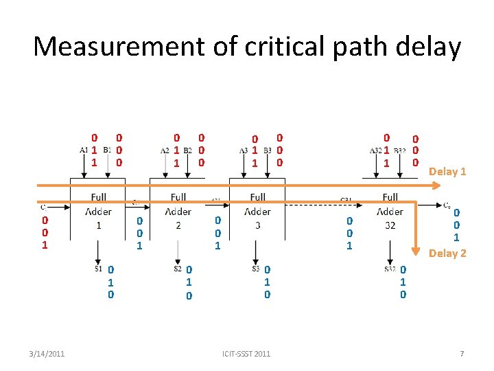
Measurement of critical path delay 0 1 1 0 0 0 0 1 1 0 0 1 0 3/14/2011 0 1 0 0 1 1 0 0 0 1 Delay 2 0 0 1 0 ICIT-SSST 2011 Delay 1 0 7
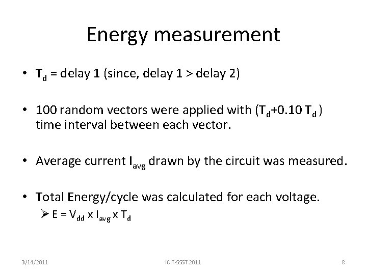
Energy measurement • Td = delay 1 (since, delay 1 > delay 2) • 100 random vectors were applied with (Td+0. 10 Td ) time interval between each vector. • Average current Iavg drawn by the circuit was measured. • Total Energy/cycle was calculated for each voltage. Ø E = Vdd x Iavg x Td 3/14/2011 ICIT-SSST 2011 8
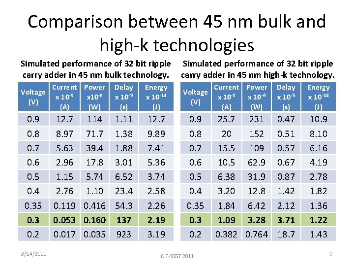
Comparison between 45 nm bulk and high-k technologies Simulated performance of 32 bit ripple carry adder in 45 nm bulk technology. Simulated performance of 32 bit ripple carry adder in 45 nm high-k technology. Voltage (V) Current Power x 10 -5 x 10 -6 (A) (W) Delay x 10 -9 (s) Energy x 10 -14 (J) 0. 9 0. 8 0. 7 0. 6 0. 5 0. 4 0. 35 0. 3 0. 2 12. 7 114 8. 97 71. 7 5. 63 39. 4 2. 96 17. 8 1. 15 5. 74 2. 76 1. 10 0. 119 0. 416 0. 053 0. 160 0. 017 0. 035 1. 11 1. 38 1. 88 3. 01 6. 52 23. 4 54. 3 137 923 12. 7 9. 89 7. 41 5. 36 3. 74 2. 58 2. 26 2. 19 3. 19 0. 8 0. 7 0. 6 0. 5 0. 4 0. 35 0. 3 0. 2 25. 7 231 20 152 15. 5 109 10. 5 62. 9 6. 38 31. 9 3. 20 12. 8 1. 84 6. 42 1. 09 3. 28 0. 382 0. 764 0. 47 0. 51 0. 57 0. 67 0. 87 1. 42 2. 12 3. 71 18. 7 10. 9 8. 10 6. 16 4. 19 2. 78 1. 82 1. 36 1. 22 1. 43 3/14/2011 ICIT-SSST 2011 9
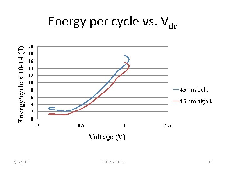
Energy/cycle x 10 -14 (J) Energy per cycle vs. Vdd 20 18 16 14 12 10 8 6 4 2 0 45 nm bulk 45 nm high k 0 0. 5 1 1. 5 Voltage (V) 3/14/2011 ICIT-SSST 2011 10
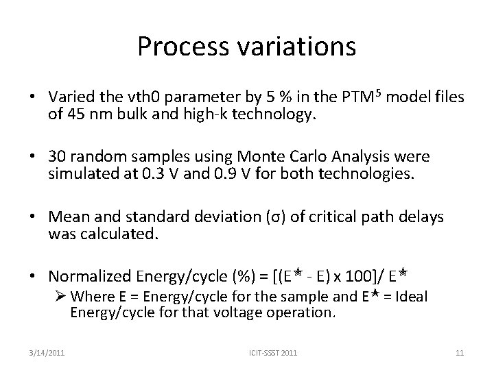
Process variations • Varied the vth 0 parameter by 5 % in the PTM 5 model files of 45 nm bulk and high-k technology. • 30 random samples using Monte Carlo Analysis were simulated at 0. 3 V and 0. 9 V for both technologies. • Mean and standard deviation (σ) of critical path delays was calculated. • Normalized Energy/cycle (%) = [(E✭ - E) x 100]/ E✭ Ø Where E = Energy/cycle for the sample and E✭ = Ideal Energy/cycle for that voltage operation. 3/14/2011 ICIT-SSST 2011 11
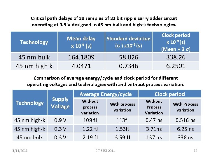
Critical path delays of 30 samples of 32 bit ripple carry adder circuit operating at 0. 3 V designed in 45 nm bulk and high-k technologies. Technology Mean delay x 10 -9 (s) Standard deviation (σ ) x 10 -9 (s) Clock period x 10 -9 (s) (Mean + 3 σ) 45 nm bulk 45 nm high k 164. 1809 4. 0471 58. 026 0. 7346 338. 26 6. 2501 Comparison of average energy/cycle and clock period for different operating voltages and technologies with and without process variation. Technology Supply Voltage 45 nm high-k 45 nm bulk 0. 9 V 0. 3 V 3/14/2011 Average Energy/cycle Clock period Without process variation Without Process Variation With Process variation 109 f. J 1. 22 f. J 2. 19 f. J 113 f. J 1. 53 f. J 3. 59 f. J 0. 47 ns 3. 71 ns 137 ns 0. 516 ns 6. 25 ns 338 ns ICIT-SSST 2011 12
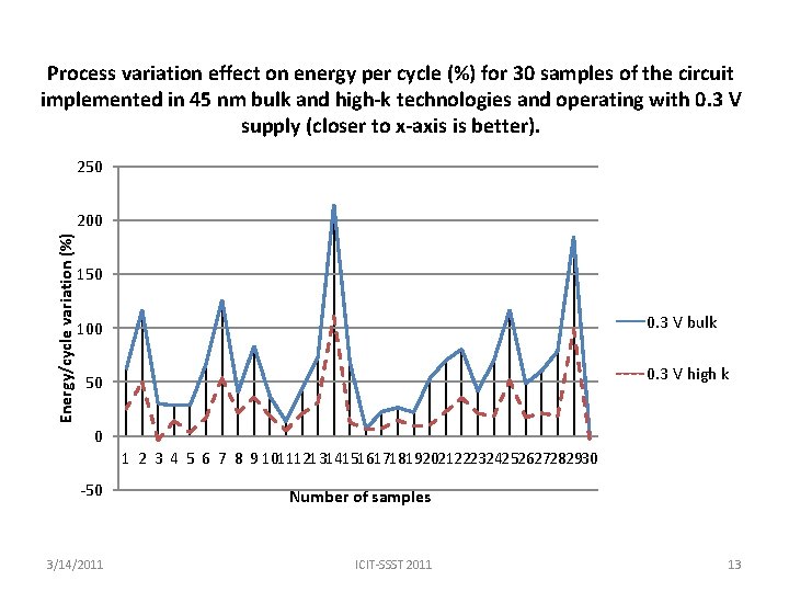
Process variation effect on energy per cycle (%) for 30 samples of the circuit implemented in 45 nm bulk and high-k technologies and operating with 0. 3 V supply (closer to x-axis is better). 250 Energy/cycle variation (%) 200 150 0. 3 V bulk 100 0. 3 V high k 50 0 1 2 3 4 5 6 7 8 9 101112131415161718192021222324252627282930 -50 Number of samples 3/14/2011 ICIT-SSST 2011 13
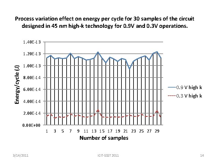
Process variation effect on energy per cycle for 30 samples of the circuit designed in 45 nm high-k technology for 0. 9 V and 0. 3 V operations. 1. 40 E-13 Energy/cycle (J) 1. 20 E-13 1. 00 E-13 8. 00 E-14 0. 9 V high k 6. 00 E-14 0. 3 V high k 4. 00 E-14 2. 00 E-14 0. 00 E+00 1 3 5 7 9 11 13 15 17 19 21 23 25 27 29 Number of samples 3/14/2011 ICIT-SSST 2011 14
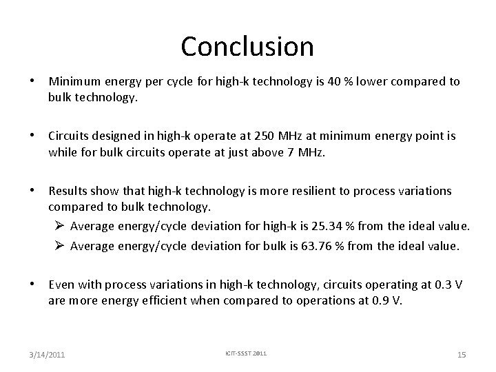
Conclusion • Minimum energy per cycle for high-k technology is 40 % lower compared to bulk technology. • Circuits designed in high-k operate at 250 MHz at minimum energy point is while for bulk circuits operate at just above 7 MHz. • Results show that high-k technology is more resilient to process variations compared to bulk technology. Ø Average energy/cycle deviation for high-k is 25. 34 % from the ideal value. Ø Average energy/cycle deviation for bulk is 63. 76 % from the ideal value. • Even with process variations in high-k technology, circuits operating at 0. 3 V are more energy efficient when compared to operations at 0. 9 V. 3/14/2011 ICIT-SSST 2011 15
References 1. 2. 3. 4. 5. 6. J. D. Meindl, and R. M. Swanson, “Potential Improvements in Power Speed Performance of Digital Circuits, ” Proc. IEEE, vol. 59, no. 5, pp. 815– 816, May 1971. M. T. Bohr, R. S. Chau, T. Ghani, and K. Mistry, “The High-k Solution, ” IEEE Spectrum, vol. 44, no. 10, pp. 29 -35, 2007. B. H. Calhoun, and A. Chandrakasan, “Ultra-Dynamic Voltage Scaling Using Sub-Threshold Operation and Local Voltage Dithering in 90 nm CMOS, ” Proc. IEEE International Solid-State Circuits Conference, pp. 300301, Feb. 2005. K. Kim, and V. D. Agrawal, “True Minimum Energy Design Using Dual Below-Threshold Supply Voltages, ” in Proc. 24 th International Conference on VLSI Design, Jan. 2011. M. Kulkarni, and V. D. Agrawal, “Energy Source Lifetime Optimization for a Digital System through Power Management, ” Proc. 43 rd Southeastern Symposium on System Theory, March 2011. PTM website, Arizona State University, http: //ptm. asu. edu/ 3/14/2011 ICIT-SSST 2011 16

Thank You!!! 3/14/2011 ICIT-SSST 2011 17
- Slides: 17