Subthreshold Design of Ultra Low Power CMOS Circuits

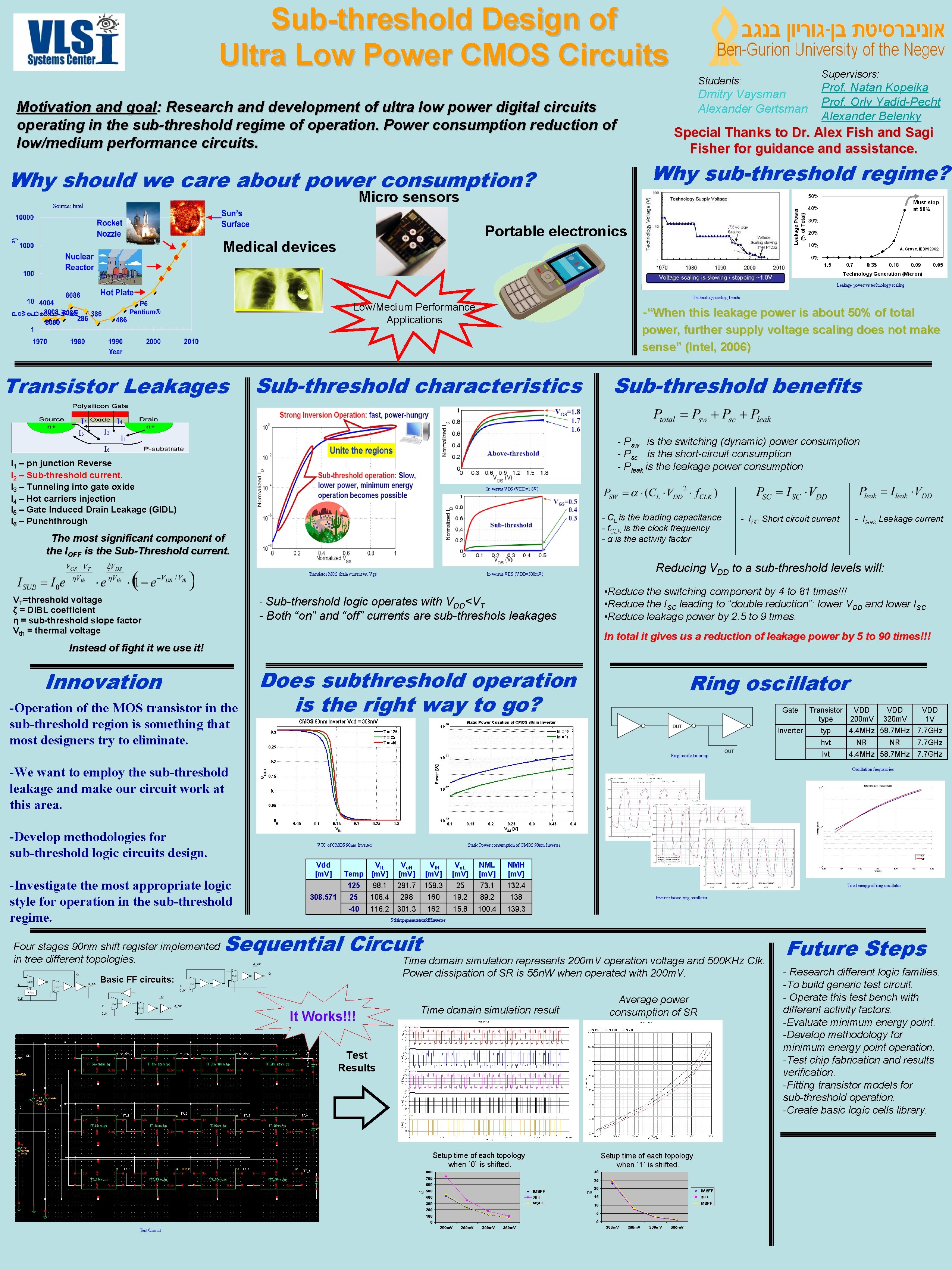
Sub-threshold Design of Ultra Low Power CMOS Circuits Supervisors: Students: Dmitry Vaysman Alexander Gertsman Motivation and goal: Research and development of ultra low power digital circuits operating in the sub-threshold regime of operation. Power consumption reduction of low/medium performance circuits. Prof. Natan Kopeika Prof. Orly Yadid-Pecht Alexander Belenky Special Thanks to Dr. Alex Fish and Sagi Fisher for guidance and assistance. Why sub-threshold regime? Why should we care about power consumption? Micro sensors Portable electronics Medical devices Leakage power vs technology scaling Technology scaling trends Low/Medium Performance Applications Transistor Leakages I 3 I 5 -“When this leakage power is about 50% of total power, further supply voltage scaling does not make sense” (Intel, 2006) Sub-threshold characteristics Sub-threshold benefits I 4 I 2 I 1 - Psw is the switching (dynamic) power consumption - Psc is the short-circuit consumption - Pleak is the leakage power consumption I 6 I 1 – pn junction Reverse I 2 – Sub-threshold current. I 3 – Tunneling into gate oxide I 4 – Hot carriers injection I 5 – Gate Induced Drain Leakage (GIDL) I 6 – Punchthrough ID versus VDS (VDD=1. 8 V) - CL is the loading capacitance - f. CLK is the clock frequency - α is the activity factor The most significant component of the IOFF is the Sub-Threshold current. Transistor MOS drain current vs. Vgs • Reduce the switching component by 4 to 81 times!!! • Reduce the ISC leading to “double reduction”: lower VDD and lower ISC • Reduce leakage power by 2. 5 to 9 times. - Both “on” and “off” currents are sub-threshols leakages In total it gives us a reduction of leakage power by 5 to 90 times!!! Instead of fight it we use it! Innovation -Operation of the MOS transistor in the sub-threshold region is something that most designers try to eliminate. Does subthreshold operation is the right way to go? Ring oscillator -We want to employ the sub-threshold leakage and make our circuit work at this area. -Develop methodologies for sub-threshold logic circuits design. Inverter typ lvt VDD 200 m. V VDD 320 m. V VDD 1 V 4. 4 MHz 58. 7 MHz 7. 7 GHz NR NR 7. 7 GHz 4. 4 MHz 58. 7 MHz 7. 7 GHz Static Power consumption of CMOS 90 nm Inverter Vdd [m. V] 308. 571 Temp VIL [m. V] Vo. H [m. V] VIH [m. V] Vo. L [m. V] NMH [m. V] 125 98. 1 291. 7 159. 3 25 73. 1 132. 4 25 108. 4 298 160 19. 2 89. 2 138 -40 116. 2 301. 3 162 15. 8 100. 4 139. 3 Total energy of ring oscillator Inverter based ring oscillator Static parameters ofof Inverter Sequential Circuit Time domain simulation represents 200 m. V operation voltage and 500 KHz Clk. Power dissipation of SR is 55 n. W when operated with 200 m. V. Basic FF circuits: It Works!!! Average power consumption of SR Time domain simulation result Test Results Setup time of each topology when `0` is shifted. ns Test Circuit Transistor type Oscillation frequencies VTC of CMOS 90 nm Inverter -Investigate the most appropriate logic style for operation in the sub-threshold regime. Gate hvt Ring oscillator setup Four stages 90 nm shift register implemented in tree different topologies. - Ileak Leakage current Reducing VDD to a sub-threshold levels will: ID versus VDS (VDD=500 m. V) - Sub-thershold logic operates with VDD<VT VT=threshold voltage ζ = DIBL coefficient η = sub-threshold slope factor Vth = thermal voltage - ISC Short circuit current Setup time of each topology when `1` is shifted. ns Future Steps - Research different logic families. -To build generic test circuit. - Operate this test bench with different activity factors. -Evaluate minimum energy point. -Develop methodology for minimum energy point operation. -Test chip fabrication and results verification. -Fitting transistor models for sub-threshold operation. -Create basic logic cells library.
- Slides: 1