Subcircuits Example subcircuits Each consists of one or

Subcircuits Example subcircuits Each consists of one or more transistors. They are not used by themselves.

Subcircuits • • • Switches Diodes/active resistors Current mirrors Current sources/current sinks Current/voltage references Band gap references

MOS switches Ideal Switch MOS transistor as a switch

Non-idealities in a switch

Simple approximation On operation: VG >> VS or VD, VDS small, triode A RON B Off operation: VGS < VT , cutoff A B Very good off-char


Observations: • RON depends on W, L, VG, VT, VDS, etc • RON is nonlinear (depending on signal) Want: RON small and constant Strategies: • Use large W and small L to reduce RON • Use large VGS to reduce the effect of signal dependency • Use bootstrapping to increase VGS beyond VDD–VSS • Use constant VGS • Use constant VB so as to have fixed VT

Effects of switch non-idealities • Finite ON Resistance – Non-zero charging and discharging time – Limit settling – Limits conversion rate Ideally: instantaneous charging Actually: takes time

• Signal level dependence of RON – Different settling behavior at different signal levels – Introduces nonlinearity – Generate higher order harmonics Vin: pure sine wave VC 1: has harmonic distortions

• Finite OFF Current – Leakage of a held voltage – Coupling through the switch – Accumulates with time

Clock Feed through
 Assume:")
EXAMPLE - Switched Capacitor Integrator (slow clock edge) Assume:

At t 2: At t 3: Once M 2 turns on at t 3, all charge on C 1 is transferred to C 2

Between t 3 and t 4 additional charge is transferred to C 1 from the channel capacitance of M 2. At t 4: Ideal transfer: Total error:

Charge injection When switch is turned off suddenly, charges trapped in the channel injected both either D and S side equally. The amount of trapped charges depends on the slope of VG

=U slow regime: L Hold value error on CL:

In the fast edge regime: Hold voltage error on CL: Study the example in the book

Dummy transistor to cancel clock feed through Complete cancellation is difficult. Requires a complementary clock.
 Larger dynamic range. 2. ) Lower ON resistance.")
Use CMOS switches Advantages 1. ) Larger dynamic range. 2. ) Lower ON resistance. Disadvantages 1. ) Requires complementary clock. 2. ) Requires more area.

Voltage doubler for gate overdrive t 1 t 2

Constant VGS Bootstrapping f=0 f=1 VDD VG=0 VGS~VDD

When f=1: Cp: total parasitic capacitance connected to top plate of C 3.

on PMOS version off

Concept: Switched cap implementation

Summary on Switches • To reduce RON – Use large W and small L – Use CMOS instead of NMOS or PMOS – Use large |VGS| • To reduce clock feed through – Use cascode – Use dummy transistor • To reduce charge injection – Use dummy – Use slow clock edge – Use complementary clock on switch and dummy • To improve linearity – Use large |VGS| – Use vin-independent VGS – Use vin-independent VBS (PMOS switch)

Diodes And Active Resistors • • Simple diode connection Voltage divider Extending the dynamic range Parallel MOSFET resistor – Extending the dynamic range • Differential resistor – Single MOSFET – Double MOSFET

Diode Connection VDS = VGS Always in saturation If v > VT, i > 0 else i = 0 diode i VT v

Generally, gm ≈ 10 gmbs ≈ 100 gds If VBS=0,

Voltage Division Equating i. D 1 to i. D 2 results in: VDS 1 +VDS 2 = VDD - VSS Can use different W/L ratio to achieve desired voltage division Use less power than resistive divider
/2 =2 gm 1=gm 2=b. VEB=10*0. 2=2 m Ro=1/4")
Active vs passive resistors Suppose Vo=(VDD+VSS)/2 =2 gm 1=gm 2=b. VEB=10*0. 2=2 m Ro=1/4 m = 250 ohm Ro =0 Io=b/2 *(VEB)2=0. 2 m. A To achieve the same Ro, need two 500 ohm resistors. Io=2/(2*500)=2 m. A, Ro 10 times Consumes 10 times more power

Current sources / sinks V Current source I I Current sink I V V

Non-ideal current sources / sinks

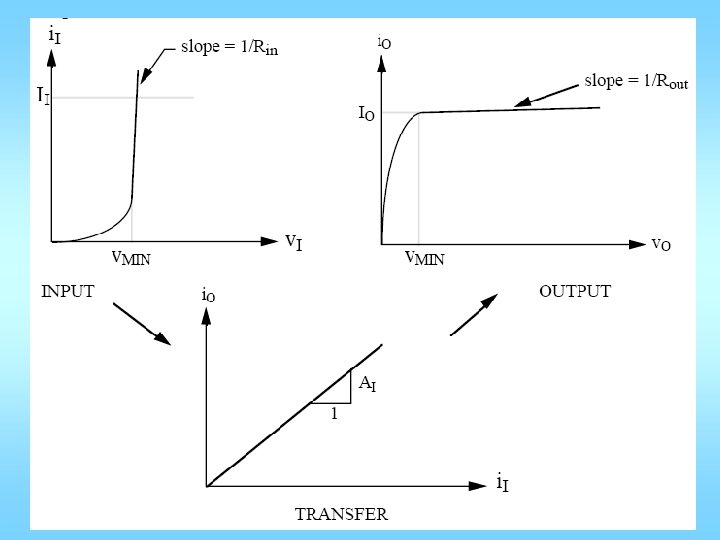
Two critical figures of merit How flat the operating portion is How small the non-operating region is rout and vmin For the simple sink on prev slide:

Increasing Rout

Cascode Current Sink

Very flat Too large

Reduction of VMIN rout ≈ rds 1*gm 2 rds 2 is large which is good But vmin = v. T +2 VON needs to be reduced

Both just saturating But the 2 IREFs must be the same. How?

M 6 is ¼ the size, it requires 2 times over drive, or 2 times VEB, or 2 time VON Very flat VMIN is much smaller

Alternative method M 5 is ¼ the size Again, the 2 IREFs must be the same.

VON ≈ 0. 6 V Larger W/L ratio can significantly reduce VON

Matching Improved by Adding M 3 Why is it better now?

Regulated Cascode Current Sink Near triode, VDS 3↓, iout ↓, VGS 4 ↓, VD 4 or VG 5 ↑, Iout ↑.

HW: As we pointed out, the circuit on the previous page suffers from a large Vmin. 1. Modify the circuit to reduce Vmin without affecting rout. 2. Once you do that, VDS for M 1 and M 2 are no longer match. Introduce another modification so that the VDSs are matched.


Current Mirrors/Current Amplifiers

Simple Current Mirrors Assuming square law model:

Simplest example

Use of transistor W to control current gains

If m. Cox and VT matched: If v. DS matched: Current gain or mirror gain is controlled by geometric ratio, which can be made quite accurate

Sources of Errors • Mismatches in W/L ratios – Use large W, L – PLI • Mismatches in m. Cox – Large area, common centroid, higher order gradient cancellation • Mismatches in v. DS – Make v. DS the same • Mismatches in VT – Large area, cancel gradient, same VBS

l effect:

VT mismatch effect:

Sensitivity A systematic way of computing errors. r=

Note: common mode errors do not contribute to matching errors, only differential errors do Therefore, can take:

Strategies to reduce errors • Matching layout – PLI, common centroid, symmetry, gradient, … – Increased area • Matching operating conditions – VD, VS, VB, current densities, … use cascoding to fix VDS • Reduce the sensitivies – Use large VGS-VT – Make equivalent l small, make go small, use cascoding to reduce go

Straightforward layout to achieve mirror ratio of 4: Matching accuracy not good.

S G G S G G S Will have better matching But: only approximate common centroid no pli can be more compact HW: suggest a better layout for ratio of 4.

Cascoding M 1 and M 2 are the mirror pair that determines io. VDS 1 and VDS 2 matched go is small

Small signal model

Wilson Current Mirror go is small VDS 1 and VDS 2 not matched

Small signal circuit

Computation of rout

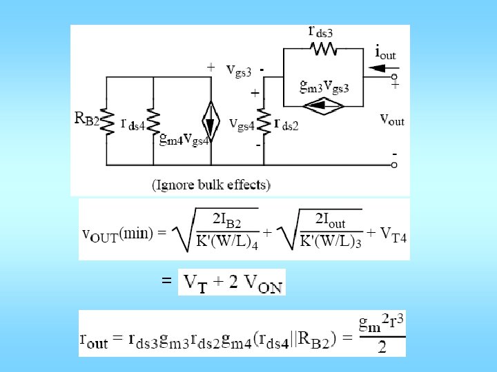
Improved Wilson Current Mirror

HW: In the improved Wilson current mirror: What is rout? What is Vmin? The resistance from D 2 to GND is 1/gm which is small. Why not connect G 2 to a constant bias to increase that impedance?

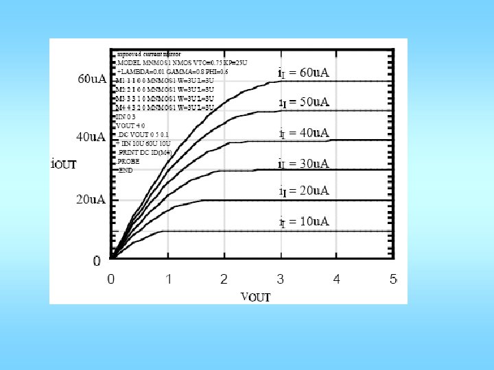
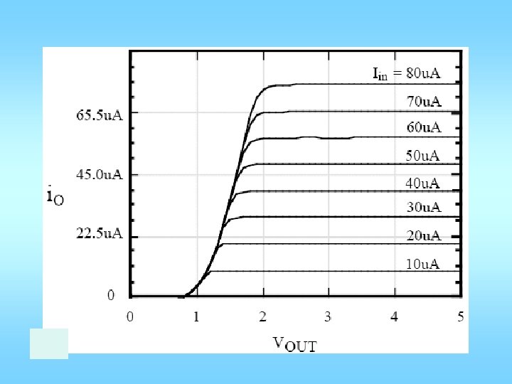
SPICE simulation

Regulated Cascode Current Mirror Same as the regulated cascoded curren sink VDS 2 is very stable with respect to vo, but not insensitive to Ireg change, not necessarily better matching

Implementation of IREG using a simple current mirror

Applications of current mirrors Common source amplifier: Load for C. S. Amp
")
Common drain amplifier (source follower)

Differential input single-ended output gain stage

- Slides: 76