Strip layers design first considerations Lorenzo Vitale on

- Slides: 40

Strip layers design: first considerations Lorenzo Vitale on behalf of the Trieste Super. B group: M. Bomben, L. Bosisio, P. Cristaudo, L. Lanceri, I. Rashevskaya, A. Starodubtsev University and INFN Trieste

Summary • Introduction 1. SVT Baseline geometry 2. Background studies 3. Front end chip candidate: FSSR 2 from BTEV • Can FSSR 2 stand the bkg rate? @ L 1 still around 0. 7 -1. 0 Mhz/cm 2 • Is its signal-to-noise adequate for the external layers? • Conclusions 9/16/2020 Super. B General Meeting - Lorenzo Vitale 2

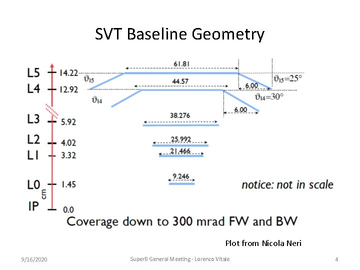
Geometry • The baseline is to assume Ba. Bar SVT with two main modifications: – Symmetrical layout – Angular coverage down to 300 mrad FW and BW 9/16/2020 Super. B General Meeting - Lorenzo Vitale 3

SVT Baseline Geometry Plot from Nicola Neri 9/16/2020 Super. B General Meeting - Lorenzo Vitale 4

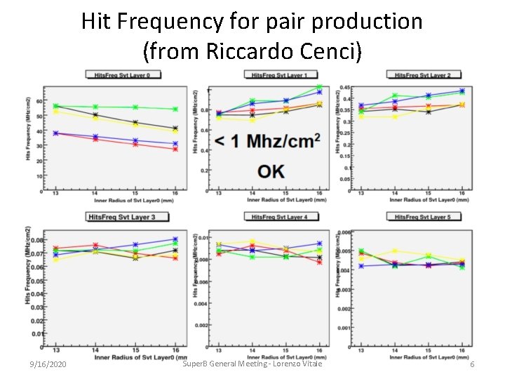
Background Studies • Riccardo Cenci made a full simulation study (Bruno) with 40 k events from the main know background (pair production) with this geometry and 5 configurations: 1. BP (Beam Pipe) close to L 0, BP inner radius is equal to the inner L 0 one minus 3 mm (BP thickness + clearance + pin-wheel average) 2. like black one, with the gold foil moved from BP to inner L 0 surface 3. BP inner radius fixed at 10 mm 4. like green one but the gold foil moved on inner L 0 surface 5. like black but the gold foil is both on the BP and on L 0 inner surface 9/16/2020 Super. B General Meeting - Lorenzo Vitale 5

Hit Frequency for pair production (from Riccardo Cenci) 9/16/2020 Super. B General Meeting - Lorenzo Vitale 6

Super. B Front end chip candidate In the CDR we identified the second release of the Fermilab Silicon Strip Readout chip (FSSR 2) as a good candidate for the L 1 -5 silicon strip detectors (also L 0 striplets). The chip was developed by Fermilab (Digital: R. Yarema, J. Hoff, A. Mekkaoui) and INFN-Pavia (Analog: V. Re, M. Manghisoni, L. Ratti) • FSSR 2 is completely data driven and data-push (zero suppression) and it can also allow direct use of the detector info in the trigger • 128 analog channels, but no analog storage, only digital output for fast data output: address, time, and 3 bit amplitude information for all hits above threshold 9/16/2020 Super. B General Meeting - Lorenzo Vitale 7

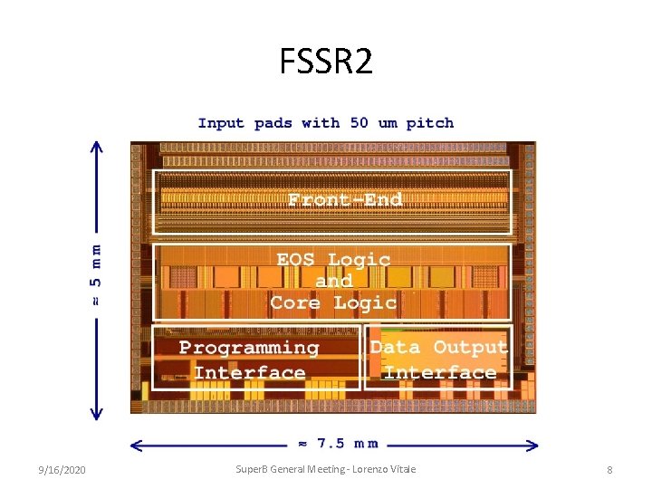
FSSR 2 9/16/2020 Super. B General Meeting - Lorenzo Vitale 8

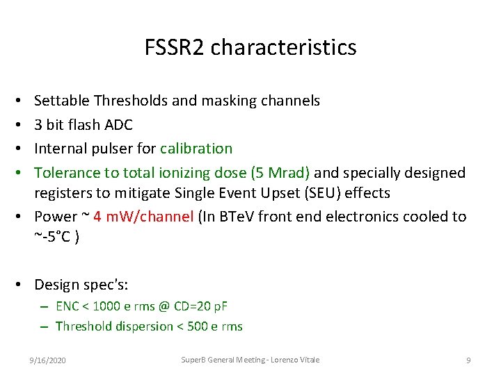
FSSR 2 characteristics Settable Thresholds and masking channels 3 bit flash ADC Internal pulser for calibration Tolerance to total ionizing dose (5 Mrad) and specially designed registers to mitigate Single Event Upset (SEU) effects • Power ~ 4 m. W/channel (In BTe. V front end electronics cooled to ~-5°C ) • • • Design spec's: – ENC < 1000 e rms @ CD=20 p. F – Threshold dispersion < 500 e rms 9/16/2020 Super. B General Meeting - Lorenzo Vitale 9

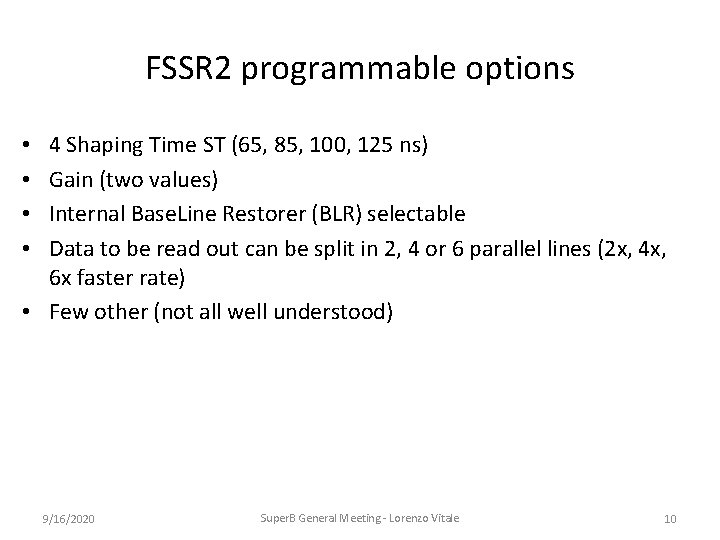
FSSR 2 programmable options 4 Shaping Time ST (65, 85, 100, 125 ns) Gain (two values) Internal Base. Line Restorer (BLR) selectable Data to be read out can be split in 2, 4 or 6 parallel lines (2 x, 4 x, 6 x faster rate) • Few other (not all well understood) • • 9/16/2020 Super. B General Meeting - Lorenzo Vitale 10

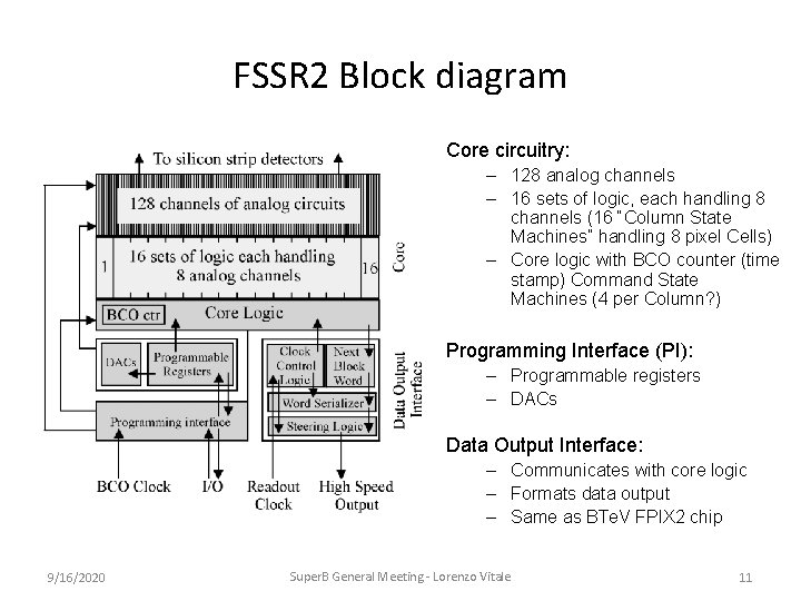
FSSR 2 Block diagram Core circuitry: – 128 analog channels – 16 sets of logic, each handling 8 channels (16 “Column State Machines” handling 8 pixel Cells) – Core logic with BCO counter (time stamp) Command State Machines (4 per Column? ) Programming Interface (PI): – Programmable registers – DACs Data Output Interface: – Communicates with core logic – Formats data output – Same as BTe. V FPIX 2 chip 9/16/2020 Super. B General Meeting - Lorenzo Vitale 11

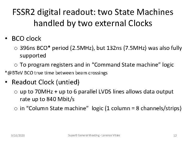
FSSR 2 digital readout: two State Machines handled by two external Clocks • BCO clock o 396 ns BCO* period (2. 5 MHz), but 132 ns (7. 5 MHz) was also fully supported o To program registers and in “Command State machine” logic *@BTe. V BCO true time between beam crossings • Readout Clock (untied) o up to 70 MHz + up to 6 parallel LVDS lines allows data output rate up to 840 Mbit/s o in “Column State machine” logic (1 column = 8 channels/strips) 9/16/2020 Super. B General Meeting - Lorenzo Vitale 12

FSSR 2 Performance Studies The present knowledge about FSSR 2 is based on: • BTe. V documentation: design, simulation studies, laboratory tests in Milano/Pavia (luckily Pavia/Bergamo are still with us) • Experience in Trieste for Super. B, starting in 2007 with the INFN SLIM 5 collaboration: – Telescope and Striplet Detectors modules, used already in 2 beam tests – first usage to read negative signals (operated successfully, with two drawbacks: higher noise and a delay) – not yet occupancy studies (planned) 9/16/2020 Super. B General Meeting - Lorenzo Vitale 13

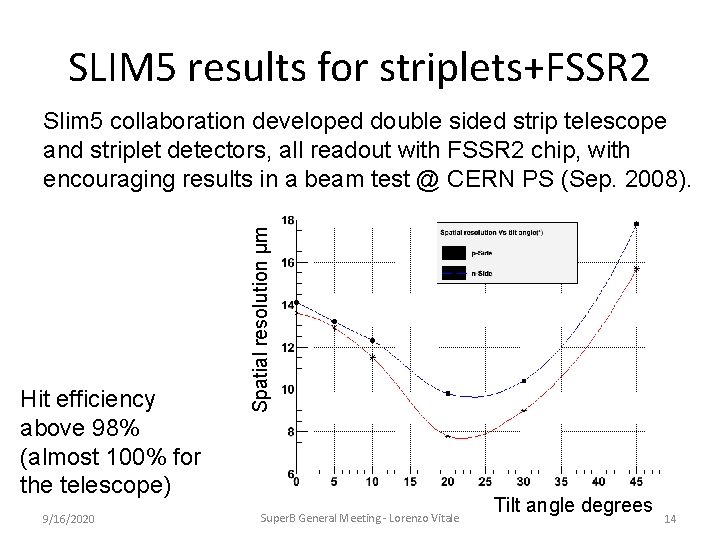
SLIM 5 results for striplets+FSSR 2 Hit efficiency above 98% (almost 100% for the telescope) 9/16/2020 Spatial resolution μm Slim 5 collaboration developed double sided strip telescope and striplet detectors, all readout with FSSR 2 chip, with encouraging results in a beam test @ CERN PS (Sep. 2008). Super. B General Meeting - Lorenzo Vitale Tilt angle degrees 14

Can FSSR 2 stand the bkg rate? INTERNAL LAYERS CONSTRAINTS: OCCUPANCY FROM BACKGROUNDS 9/16/2020 Super. B General Meeting - Lorenzo Vitale 15

Can the FSSR 2 stand the Super. B bkg rate expected in Layer 1? • In Layer 1 we can expect a FSSR 2 chip occupancy up to 7. 5%: Assuming bkg rate of 1 MHz/cm 2, 2 hit/track, 10. 7 cm strip length, 50μm pitch, including a safety factor 5 and using in the denominator 7. 5 Mhz (the maximum BCO clock foreseen for FSSR 2) • This number would be already critical for the reconstruction, but meanwhile: • Is FSSR 2 readout fast enough for Super. B? 9/16/2020 Super. B General Meeting - Lorenzo Vitale 16

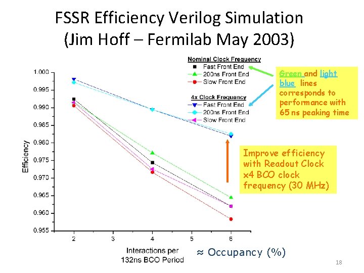
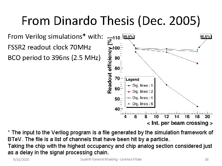
Occupancy studies • FSSR 2 chip was optimized for BTe. V operation, their simulations showed: – With 2 interactions/bunch crossing (132 ns), BTe. V FSSR 2 worst case occupancy was above 2% (chips with highest occupancy) – Verilog Simulation performed for BTe. V with 2 interactions/bunch crossing indicates: FSSR 2 can handle 2% occupancy with efficiency > 99% even with a readout clock = BCO clock – with 6 interactions/bunch (~6% occupancy? ) efficiency can be kept high enough (~ 98. 5%) with a readout clock = 30 MHz (four time faster) 9/16/2020 Super. B General Meeting - Lorenzo Vitale 17

FSSR Efficiency Verilog Simulation (Jim Hoff – Fermilab May 2003) Green and light blue lines corresponds to performance with 65 ns peaking time Improve efficiency with Readout Clock x 4 BCO clock frequency (30 MHz) ≈ Occupancy (%) 9/16/2020 Super. B General Meeting - Lorenzo Vitale 18

Remarks • Actually the FSSR 2 Readout Clock can be operated even faster than 30 MHz (up to 70 MHz, lab tests OK), but this studies should be revisited for Super. B - We need FSSR 2 simulations for Super. B • Then in case of a FSSR redesign these two aspects should be kept in mind: - Is it possible to have a faster BCO and shorter shaping time to reduce the occupancy? - Negative signals should be optimized too (delay, noise, etc) 9/16/2020 Super. B General Meeting - Lorenzo Vitale 19

Conclusions for Layer 1 FSSR 2 should be able to operate at >98. 5% efficiency with ~6% occupancy, (still ok for layer 1 with safety factor 4) • But we must operate FSSR 2 at its limits: highest BCO clock (132 ns), Readout clock at 70 MHz and 6 lines, 65 ns, BLR These aspects must be kept in mind in case of FSSR redesign Now we need: • Ad hoc simulations to revise performances and possible improvements from redesign (help from experts! is starting) • Other laboratory tests, that we plan to do in Trieste 9/16/2020 Super. B General Meeting - Lorenzo Vitale 20

Is FSSR 2 signal-to-noise adequate? EXTERNAL LAYERS CONSTRAINTS: LARGE C & RS 9/16/2020 Super. B General Meeting - Lorenzo Vitale 21

FSSR 2 Readout of SVT Layer 5 • The SVT external layers at Super. B will be longer than in Ba. Bar => higher Cload and higher RS. • To start with, we assume all other geometrical parameters of the detector to remain unchanged. • Can the FSSR 2 front-end chip (possibly with a modified analog section) provide adequate S/N performance? 9/16/2020 Super. B General Meeting - Lorenzo Vitale 22

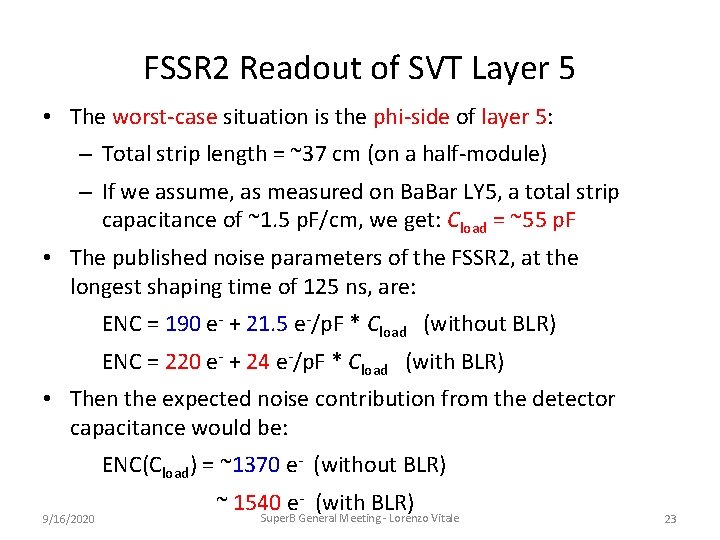
FSSR 2 Readout of SVT Layer 5 • The worst-case situation is the phi-side of layer 5: – Total strip length = ~37 cm (on a half-module) – If we assume, as measured on Ba. Bar LY 5, a total strip capacitance of ~1. 5 p. F/cm, we get: Cload = ~55 p. F • The published noise parameters of the FSSR 2, at the longest shaping time of 125 ns, are: ENC = 190 e- + 21. 5 e-/p. F * Cload (without BLR) ENC = 220 e- + 24 e-/p. F * Cload (with BLR) • Then the expected noise contribution from the detector capacitance would be: ENC(Cload) = ~1370 e- (without BLR) 9/16/2020 ~ 1540 e- (with BLR) Super. B General Meeting - Lorenzo Vitale 23

FSSR 2 Equivalent Noise Charge The BLR improves the threshold dispersion (AC coupling), but increases noise 9/16/2020 Super. B General Meeting - Lorenzo Vitale 24

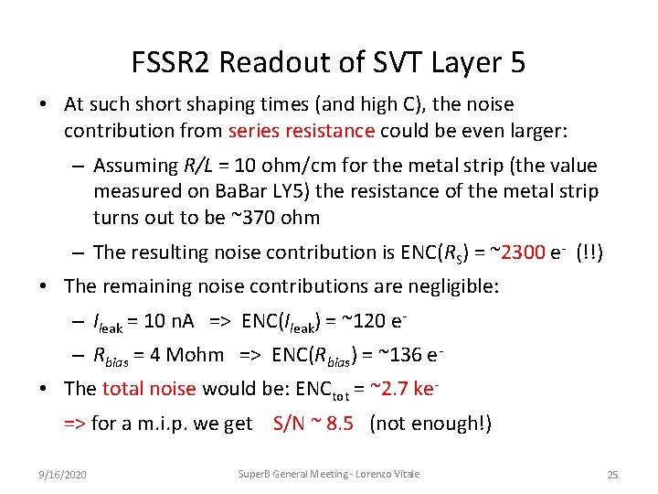
FSSR 2 Readout of SVT Layer 5 • At such short shaping times (and high C), the noise contribution from series resistance could be even larger: – Assuming R/L = 10 ohm/cm for the metal strip (the value measured on Ba. Bar LY 5) the resistance of the metal strip turns out to be ~370 ohm – The resulting noise contribution is ENC(RS) = ~2300 e- (!!) • The remaining noise contributions are negligible: – Ileak = 10 n. A => ENC(Ileak) = ~120 e– Rbias = 4 Mohm => ENC(Rbias) = ~136 e • The total noise would be: ENCtot = ~2. 7 ke=> for a m. i. p. we get S/N ~ 8. 5 (not enough!) 9/16/2020 Super. B General Meeting - Lorenzo Vitale 25

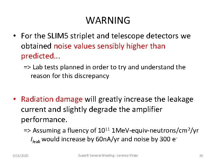
WARNING • For the SLIM 5 striplet and telescope detectors we obtained noise values sensibly higher than predicted. . . => Lab tests planned in order to try and understand the reason for this discrepancy • Radiation damage will greatly increase the leakage current and slightly degrade the amplifier performance. => Assuming a fluency of 1011 1 Me. V-equiv-neutrons/cm 2/yr Ileak would increase by 60 n. A/yr and noise by 300 e 9/16/2020 Super. B General Meeting - Lorenzo Vitale 26

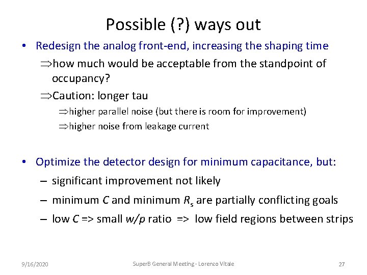
Possible (? ) ways out • Redesign the analog front-end, increasing the shaping time how much would be acceptable from the standpoint of occupancy? Caution: longer tau higher parallel noise (but there is room for improvement) higher noise from leakage current • Optimize the detector design for minimum capacitance, but: – significant improvement not likely – minimum C and minimum Rs are partially conflicting goals – low C => small w/p ratio => low field regions between strips 9/16/2020 Super. B General Meeting - Lorenzo Vitale 27

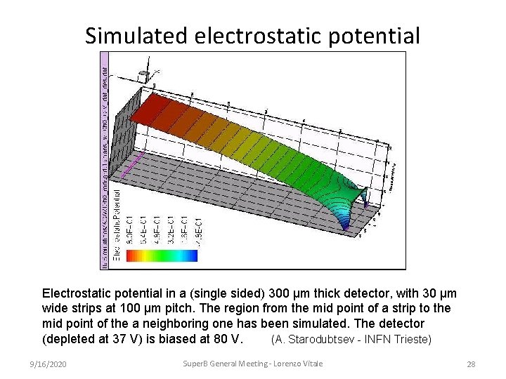
Simulated electrostatic potential Electrostatic potential in a (single sided) 300 µm thick detector, with 30 µm wide strips at 100 µm pitch. The region from the mid point of a strip to the mid point of the a neighboring one has been simulated. The detector (depleted at 37 V) is biased at 80 V. (A. Starodubtsev - INFN Trieste) 9/16/2020 Super. B General Meeting - Lorenzo Vitale 28

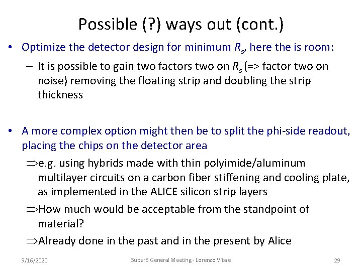
Possible (? ) ways out (cont. ) • Optimize the detector design for minimum Rs, here the is room: – It is possible to gain two factors two on Rs (=> factor two on noise) removing the floating strip and doubling the strip thickness • A more complex option might then be to split the phi-side readout, placing the chips on the detector area e. g. using hybrids made with thin polyimide/aluminum multilayer circuits on a carbon fiber stiffening and cooling plate, as implemented in the ALICE silicon strip layers How much would be acceptable from the standpoint of material? Already done in the past and in the present by Alice 9/16/2020 Super. B General Meeting - Lorenzo Vitale 29

Conclusions for Layer 5 • A preliminary, rough estimate of the expected noise appears to preclude using the present version of the FSSR 2 chip for the readout of the external SVT layers. • More refined estimates of the detector parameters will be made, and the z-side (n-side) will also be considered. • Geometry changes (strip pitch, width, thickness) can be explored with the help of simulations. • An evaluation of the possible improvement coming from a redesign of the chip analog section is needed. 9/16/2020 Super. B General Meeting - Lorenzo Vitale 30

Conclusions • The usage of the present version of the FSSR 2 chip for the strip layers of the Super. B SVT has some critical aspects even with FSSR 2 operated at its limits: – Not large safety margins on layer 1 for occupancy – Risk of having marginal S/N on layers 4 and 5 Some possible ways outs were discussed, now we must focus on: • All the aspects that should be kept in mind in case of redesign – Analog Section (Shorter & Longer ST), Negative signals, etc • Ad hoc chip simulations to revise performances and possible improvements from redesign • What we can gain from detector optimization (Trieste) • Further laboratory tests, that we plan to do in Trieste 9/16/2020 Super. B General Meeting - Lorenzo Vitale 31

Backup slides 9/16/2020 Super. B General Meeting - Lorenzo Vitale 32

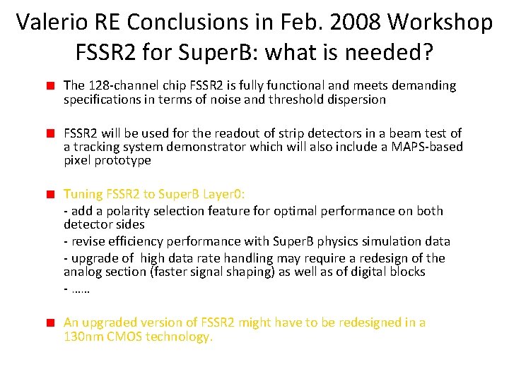
Valerio RE Conclusions in Feb. 2008 Workshop FSSR 2 for Super. B: what is needed? The 128 -channel chip FSSR 2 is fully functional and meets demanding specifications in terms of noise and threshold dispersion FSSR 2 will be used for the readout of strip detectors in a beam test of a tracking system demonstrator which will also include a MAPS-based pixel prototype Tuning FSSR 2 to Super. B Layer 0: - add a polarity selection feature for optimal performance on both detector sides - revise efficiency performance with Super. B physics simulation data - upgrade of high data rate handling may require a redesign of the analog section (faster signal shaping) as well as of digital blocks - …… An upgraded version of FSSR 2 might have to be redesigned in a 130 nm CMOS technology.

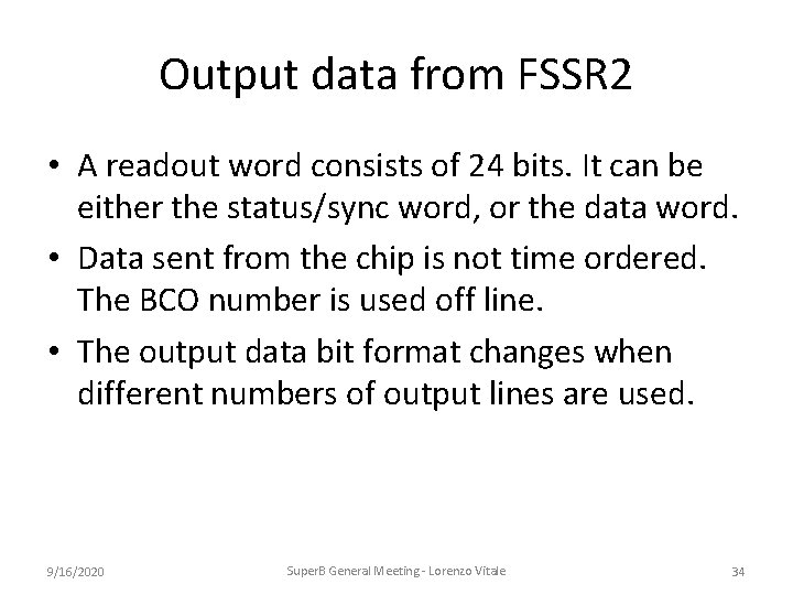
Output data from FSSR 2 • A readout word consists of 24 bits. It can be either the status/sync word, or the data word. • Data sent from the chip is not time ordered. The BCO number is used off line. • The output data bit format changes when different numbers of output lines are used. 9/16/2020 Super. B General Meeting - Lorenzo Vitale 34

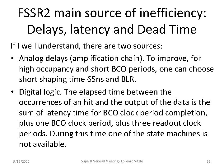
FSSR 2 main source of inefficiency: Delays, latency and Dead Time If I well understand, there are two sources: • Analog delays (amplification chain). To improve, for high occupancy and short BCO periods, one can choose short shaping time 65 ns and BLR. • Digital logic. The elapsed time between the occurrences of an hit and the output of the data is the sum of latency time for BCO clock period completion, plus one BCO clock period, plus three readout clock periods. During this time one of the state machines is not available. 9/16/2020 Super. B General Meeting - Lorenzo Vitale 35

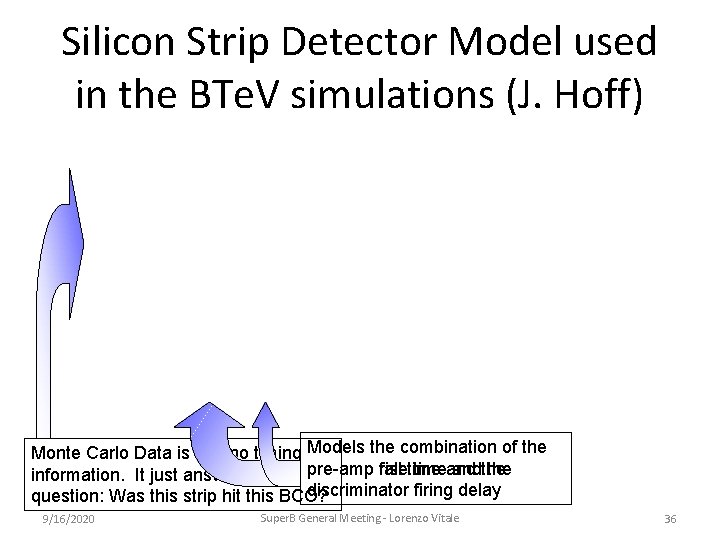
Silicon Strip Detector Model used in the BTe. V simulations (J. Hoff) Monte Carlo Data is has no timing Models the combination of the pre-amp fall risetimeand andthe information. It just answers the discriminator firing delay question: Was this strip hit this BCO? 9/16/2020 Super. B General Meeting - Lorenzo Vitale 36

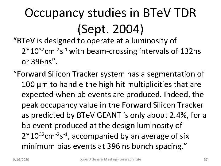
Occupancy studies in BTe. V TDR (Sept. 2004) “BTe. V is designed to operate at a luminosity of 2*1032 cm-2 s-1 with beam-crossing intervals of 132 ns or 396 ns”. “Forward Silicon Tracker system has a segmentation of 100 μm to handle the high hit multiplicities that are expected when bb events are produced. Indeed, the peak occupancy value in the Forward Silicon Tracker as predicted by BTe. V GEANT is only about 2. 4%, for a bb event produced at the design luminosity of 2*1032 cm-2 s-1, accompanied by an average of six minimum bias events at 396 ns bunch spacing. ” 9/16/2020 Super. B General Meeting - Lorenzo Vitale 37

From Dinardo Thesis (Dec. 2005) From Verilog simulations* with: FSSR 2 readout clock 70 MHz BCO period to 396 ns (2. 5 MHz) * The input to the Verilog program is a file generated by the simulation framework of BTe. V. The file is a list of channels that have been hit by a particle. Taking the chip with the highest occupancy and chip analog section considered just as a delay in the signal processing chain. 9/16/2020 Super. B General Meeting - Lorenzo Vitale 38

Other sources of inefficiency? Big events? Since the “End of Column” Logic handles 8 channels/strips (technically called “Pixel Cells”), and there are 4 sets of “Command State Machines” per Column, not clear for me how to handle more than 4 channels within one column. Are the 8 channels within a column contiguous? 9/16/2020 Super. B General Meeting - Lorenzo Vitale 39

FSSR 2 Bibliography • J. Hoff Verilog studies http: //www-btev. fnal. gov/cgibin/public/Doc. DB/Show. Document? docid=1718 • Silicon chapter in BTe. V TDR http: //www-btev. fnal. gov/Doc. DB/003752/003/siliconchapter. pdf • Dinardo Ph. D. Thesis http: //lss. fnal. gov/archive/thesis/fermilab-thesis-2005 -66. shtml • J. Hoff FPIX/FSSR 2 Core architecture http: //www-ppd. fnal. gov/EEDOffice-W/ASIC. . . /Conf-00 -260 -E. pdf 9/16/2020 Super. B General Meeting - Lorenzo Vitale 40