STREAM Overview Heinz Pernegger Experimental Physics Department CERN
- Slides: 34

STREAM Overview Heinz Pernegger Experimental Physics Department – CERN STREAM – Kickoff Meeting CERN 18 January 2016 H. Pernegger / CERN Smart Sensor Technologies and Training for Radiation Enhanced Applications and Measurements 18/1/2016 1

STREAM • The STREAM Project is the Marie Curie Innovative Training Network for CMOS Sensor Development in the context of LHC experiments and for selected industrial applications • It will provide research and training in the fields of – Physics – Electronics – Sensor Design – System integration • STREAM offers 17 positions for the Early-stage researchers • STREAM Website: http: //stream. web. cern. ch/ H. Pernegger / CERN Smart Sensor Technologies and Training for Radiation Enhanced Applications and Measurements 18/1/2016 2

STREAM Research and Training • The STREAM research and training program focuses on the development of radiation hard CMOS sensor technologies for innovative scientific and industrial instruments. • Interdisciplinary industry collaboration and research on key enabling technologies – Novel High Voltage (HV) and High-resistivity (HR) imaging (CIS, DMAPS) CMOS-based technologies and production processes. – Advanced design and layout for application specific CMOS-based smart sensors. – Innovative technology integration, implementation and qualification procedures • STREAM has also a special focus on dissemination, knowledge transfer and business studies. H. Pernegger / CERN Smart Sensor Technologies and Training for Radiation Enhanced Applications and Measurements 18/1/2016 3

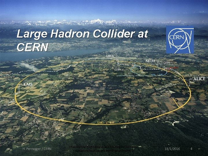
Large Hadron Collider at CERN H. Pernegger / CERN Smart Sensor Technologies and Training for Radiation Enhanced Applications and Measurements 18/1/2016 4

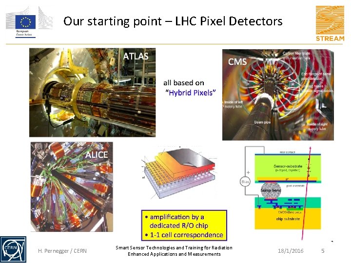
Our starting point – LHC Pixel Detectors H. Pernegger / CERN Smart Sensor Technologies and Training for Radiation Enhanced Applications and Measurements 18/1/2016 5

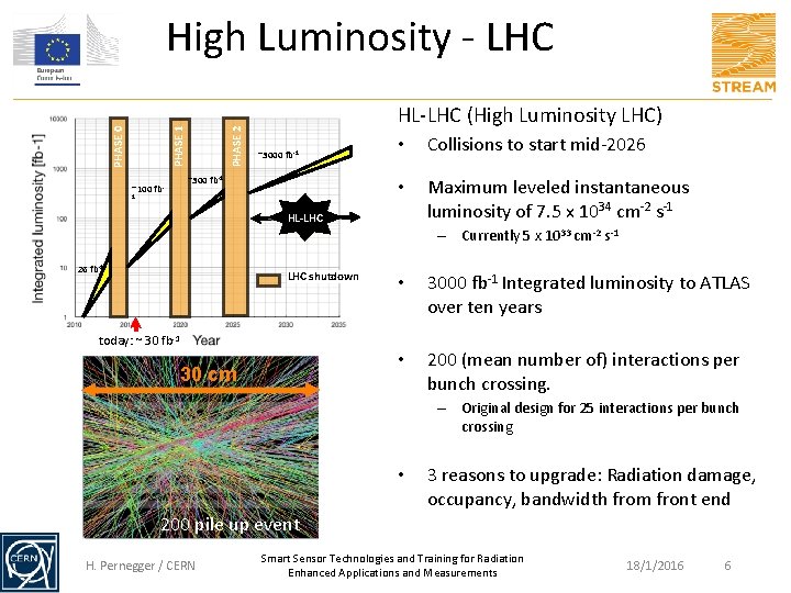
~100 fb- PHASE 2 PHASE 0 PHASE 1 High Luminosity - LHC HL-LHC (High Luminosity LHC) ~3000 fb-1 ~300 fb-1 1 • Collisions to start mid-2026 • Maximum leveled instantaneous luminosity of 7. 5 x 1034 cm-2 s-1 HL-LHC – Currently 5 x 1033 cm-2 s-1 26 fb-1 LHC shutdown today: ~ 30 fb-1 30 cm • 3000 fb-1 Integrated luminosity to ATLAS over ten years • 200 (mean number of) interactions per bunch crossing. – Original design for 25 interactions per bunch crossing • 3 reasons to upgrade: Radiation damage, occupancy, bandwidth from front end 200 pile up event H. Pernegger / CERN Smart Sensor Technologies and Training for Radiation Enhanced Applications and Measurements 18/1/2016 6

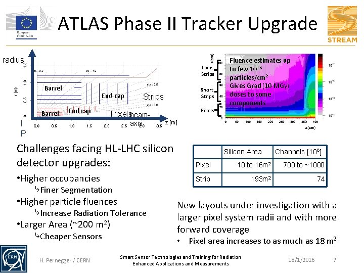
ATLAS Phase II Tracker Upgrade radius Long Strips Barrel End cap Short Strips Pixelsbeam- I P axis Fluence estimates up to few 1016 particles/cm 2 Gives Grad (10 MGy) doses to some components z [m] Challenges facing HL-LHC silicon detector upgrades: Pixel 10 to 16 m 2 700 to ~1000 • Higher occupancies Strip 193 m 2 74 Silicon Area Channels [106] ⤷Finer Segmentation • Higher particle fluences ⤷Increase Radiation Tolerance Short Strip (2. 4 cm)(~200 -stripsm(stereo layers): 2) • Larger Area Long Strip (4. 8 cm) -strips (stereo layers): ⤷Cheaper Sensors H. Pernegger / CERN New layouts under investigation with a pixel and 15 with r = larger 38, 50, 62 cm system Upradii to 1. 2 x 10 1 Me. Vmore neq/cm 2 r = forward 74, 100 cmcoverage. Up to 5. 6 x 10¹⁴ 1 Me. V neq/cm 2 • Pixel area increases to as much as 18 m 2 Smart Sensor Technologies and Training for Radiation Enhanced Applications and Measurements 18/1/2016 7

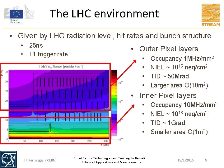
The LHC environment • Given by LHC radiation level, hit rates and bunch structure • 25 ns • L 1 trigger rate • Outer Pixel layers • • Occupancy 1 MHz/mm 2 NIEL ~ 1015 neq/cm 2 TID ~ 50 Mrad Larger area O(10 m 2) • Inner Pixel layers • • H. Pernegger / CERN Smart Sensor Technologies and Training for Radiation Enhanced Applications and Measurements Occupancy 10 MHz/mm 2 NIEL ~ 1016 neq/cm 2 TID ~ 1 Grad Smaller area O(1 m 2) 18/1/2016 8

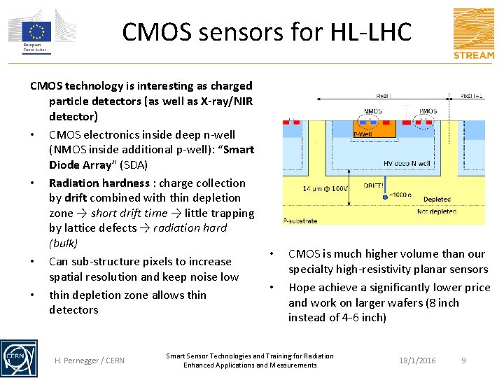
CMOS sensors for HL-LHC CMOS technology is interesting as charged particle detectors (as well as X-ray/NIR detector) • CMOS electronics inside deep n-well (NMOS inside additional p-well): “Smart Diode Array” (SDA) • Radiation hardness : charge collection by drift combined with thin depletion zone → short drift time → little trapping by lattice defects → radiation hard (bulk) • Can sub-structure pixels to increase spatial resolution and keep noise low • thin depletion zone allows thin detectors H. Pernegger / CERN • • CMOS is much higher volume than our specialty high-resistivity planar sensors Hope achieve a significantly lower price and work on larger wafers (8 inch instead of 4 -6 inch) Smart Sensor Technologies and Training for Radiation Enhanced Applications and Measurements 18/1/2016 9

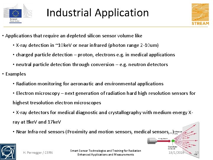
Industrial Application • Applications that require an depleted silicon sensor volume like • X-ray detection in ~10 ke. V or near infrared (photon range 2 -10 um) • charged particle detection – proton, electrons e. g. in medical applications • neutral particle detection through conversion – e. g. neutron detectors • Examples • Radiation monitoring for aeronautic and environmental applications • Electron microscopy – next generation of radiation hard high resolution sensors for highest tresolution electron microscopes • X-ray detectors for medical diagnostic and crystallography with medium energy Xray at 8 ke. V and 17 ke. V • Near Infra-red sensors (Proximity and motion sensors, medical sensors, . . ) H. Pernegger / CERN Smart Sensor Technologies and Training for Radiation Enhanced Applications and Measurements 18/1/2016 10

The STREAM challenges • Develop CMOS sensors that… – Collect charge by drift – not diffusion! – Analog designs : Demonstrated radiation hardness to high levels (1014 to 1015 to 1016 neq/cm 2) and show fast signal response (~20 ns) – Digital integration as driven by applications : Assembly to digital chip (“CCPD”) and/or integration of digital stages compatible with application specifications in monolithic sensors – System integration to detector modules using ultrafine pitch bonding and/or TSV and redistribution layers H. Pernegger / CERN Smart Sensor Technologies and Training for Radiation Enhanced Applications and Measurements 18/1/2016 11

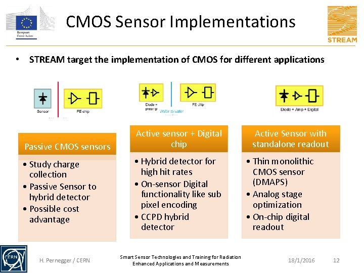
CMOS Sensor Implementations • STREAM target the implementation of CMOS for different applications Passive CMOS sensors • Study charge collection • Passive Sensor to hybrid detector • Possible cost advantage H. Pernegger / CERN Active sensor + Digital chip • Hybrid detector for high hit rates • On-sensor Digital functionality like sub pixel encoding • CCPD hybrid detector Smart Sensor Technologies and Training for Radiation Enhanced Applications and Measurements Active Sensor with standalone readout • Thin monolithic CMOS sensor (DMAPS) • Analog stage optimization • On-chip digital readout 18/1/2016 12

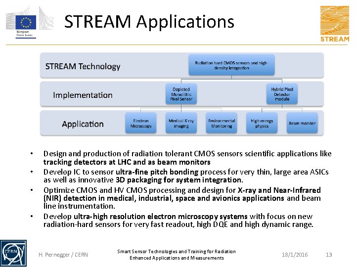
STREAM Applications • • Design and production of radiation tolerant CMOS sensors scientific applications like tracking detectors at LHC and as beam monitors Develop IC to sensor ultra-fine pitch bonding process for very thin, large area ASICs as well as innovative 3 D packaging for system integration. Optimize CMOS and HV CMOS processing and design for X-ray and Near-Infrared (NIR) detection in medical, industrial, space and avionics applications and beam line instrumentation. Develop ultra-high resolution electron microscopy systems with focus on new radiation-hard sensors for very fast readout, high DQE and high dynamic range. H. Pernegger / CERN Smart Sensor Technologies and Training for Radiation Enhanced Applications and Measurements 18/1/2016 13

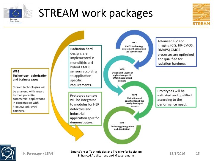
STREAM and CMOS Sensors • STREAM programme is designed to address the scientific goals and provide a training programme for the STREAM researchers. • STREAM research and training work packages on – CMOS Technologies Assessment – Smart Sensor Design and Layout – Validation and Qualification – Technology Integration – Valorization H. Pernegger / CERN Smart Sensor Technologies and Training for Radiation Enhanced Applications and Measurements 18/1/2016 14

STREAM work packages H. Pernegger / CERN Smart Sensor Technologies and Training for Radiation Enhanced Applications and Measurements 18/1/2016 15

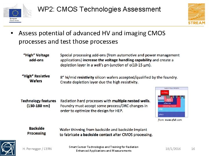
WP 2: CMOS Technologies Assessment • Assess potential of advanced HV and imaging CMOS processes and test those processes H. Pernegger / CERN Smart Sensor Technologies and Training for Radiation Enhanced Applications and Measurements 18/1/2016 16

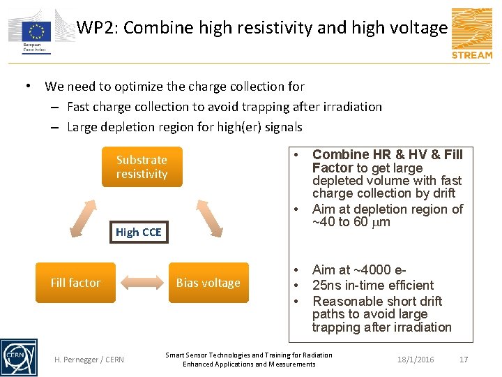
WP 2: Combine high resistivity and high voltage • We need to optimize the charge collection for – Fast charge collection to avoid trapping after irradiation – Large depletion region for high(er) signals • Substrate resistivity • High CCE Fill factor H. Pernegger / CERN Bias voltage • • • Combine HR & HV & Fill Factor to get large depleted volume with fast charge collection by drift Aim at depletion region of ~40 to 60 m Aim at ~4000 e 25 ns in-time efficient Reasonable short drift paths to avoid large trapping after irradiation Smart Sensor Technologies and Training for Radiation Enhanced Applications and Measurements 18/1/2016 17

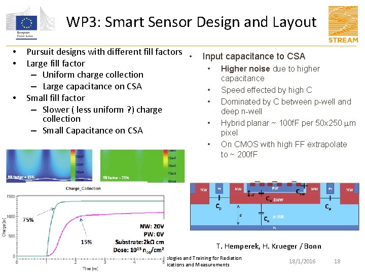
WP 3: Smart Sensor Design and Layout • • • Pursuit designs with different fill factors • Large fill factor – Uniform charge collection – Large capacitance on CSA Small fill factor – Slower ( less uniform ? ) charge collection – Small Capacitance on CSA Input capacitance to CSA • • • Higher noise due to higher capacitance Speed effected by high C Dominated by C between p-well and deep n-well Hybrid planar ~ 100 f. F per 50 x 250 m pixel On CMOS with high FF extrapolate to ~ 200 f. F T. Hemperek, H. Krueger / Bonn H. Pernegger / CERN Smart Sensor Technologies and Training for Radiation Enhanced Applications and Measurements 18/1/2016 18

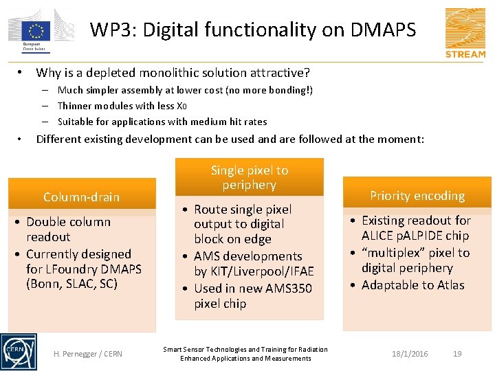
WP 3: Digital functionality on DMAPS • Why is a depleted monolithic solution attractive? – Much simpler assembly at lower cost (no more bonding!) – Thinner modules with less X 0 – Suitable for applications with medium hit rates • Different existing development can be used and are followed at the moment: Column-drain • Double column readout • Currently designed for LFoundry DMAPS (Bonn, SLAC, SC) H. Pernegger / CERN Single pixel to periphery Priority encoding • Route single pixel output to digital block on edge • AMS developments by KIT/Liverpool/IFAE • Used in new AMS 350 pixel chip • Existing readout for ALICE p. ALPIDE chip • “multiplex” pixel to digital periphery • Adaptable to Atlas Smart Sensor Technologies and Training for Radiation Enhanced Applications and Measurements 18/1/2016 19

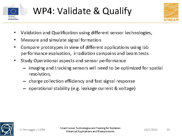
WP 4: Validate & Qualify • Validation and Qualification using different sensor technologies, • Measure and simulate signal formation • Compare prototypes in view of different applications using lab performance evaluation, irradiation campains and beam tests • Study Operational aspects and sensor performance – imaging and tracking sensors will need to be optimized for spatial resolution, – charge collection efficiency and fast signal response – operational stability (e. g. leakage current & voltage) H. Pernegger / CERN Smart Sensor Technologies and Training for Radiation Enhanced Applications and Measurements 18/1/2016 20

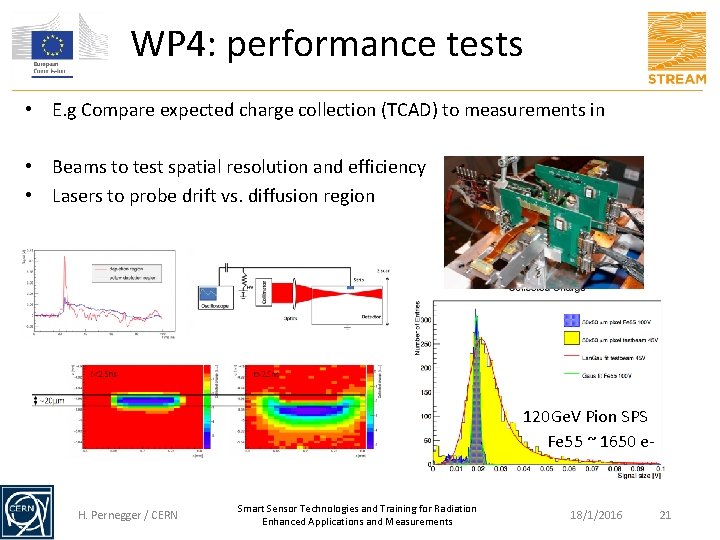
WP 4: performance tests • E. g Compare expected charge collection (TCAD) to measurements in • Beams to test spatial resolution and efficiency • Lasers to probe drift vs. diffusion region 120 Ge. V Pion SPS Fe 55 ~ 1650 e- H. Pernegger / CERN Smart Sensor Technologies and Training for Radiation Enhanced Applications and Measurements 18/1/2016 21

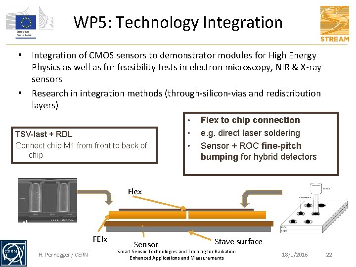
WP 5: Technology Integration • Integration of CMOS sensors to demonstrator modules for High Energy Physics as well as for feasibility tests in electron microscopy, NIR & X-ray sensors • Research in integration methods (through-silicon-vias and redistribution layers) TSV-last + RDL Connect chip M 1 from front to back of chip • • • Flex to chip connection e. g. direct laser soldering Sensor + ROC fine-pitch bumping for hybrid detectors Flex leti FEIx H. Pernegger / CERN Sensor Stave surface Smart Sensor Technologies and Training for Radiation Enhanced Applications and Measurements 18/1/2016 22

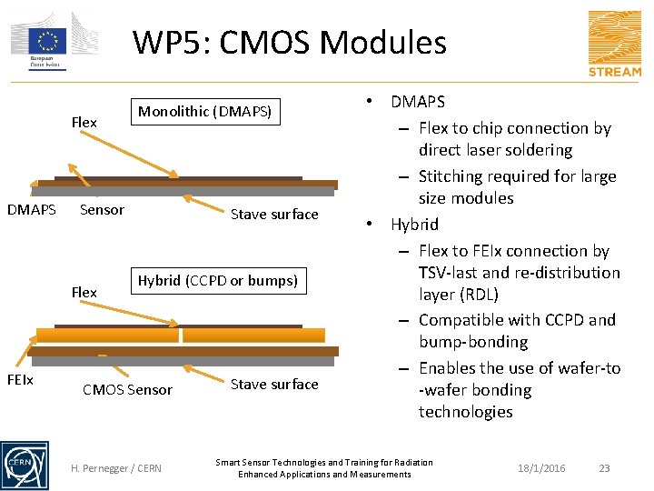
WP 5: CMOS Modules Flex DMAPS Sensor Flex FEIx Monolithic (DMAPS) Stave surface Hybrid (CCPD or bumps) CMOS Sensor H. Pernegger / CERN Stave surface • DMAPS – Flex to chip connection by direct laser soldering – Stitching required for large size modules • Hybrid – Flex to FEIx connection by TSV-last and re-distribution layer (RDL) – Compatible with CCPD and bump-bonding – Enables the use of wafer-to -wafer bonding technologies Smart Sensor Technologies and Training for Radiation Enhanced Applications and Measurements 18/1/2016 23

W 6: Valorization Stream technologies will be analysed with regard to their potential commercial applications in cooperation with STREAM industrial partners: • Technological competence leveraging : identification and evaluation of application fields for STREAM technologies • Market studies, business model development and commercialization strategies A hands-on entrepreneurship training program will be offered to the ESRs , providing them with the opportunity to work on business cases for STREAM technologies themselves. H. Pernegger / CERN Smart Sensor Technologies and Training for Radiation Enhanced Applications and Measurements 18/1/2016 24

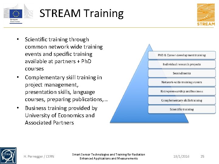
STREAM Training • Scientific training through common network wide training events and specific training available at partners + Ph. D courses • Complementary skill training in project management, presentation skills, language courses, preparing publications, … • Business training provided by University of Economics and Associated Partners H. Pernegger / CERN Smart Sensor Technologies and Training for Radiation Enhanced Applications and Measurements 18/1/2016 25

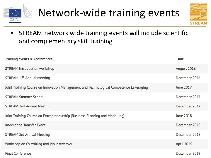
Network-wide training events • STREAM network wide training events will include scientific and complementary skill training H. Pernegger / CERN Smart Sensor Technologies and Training for Radiation Enhanced Applications and Measurements 18/1/2016 26

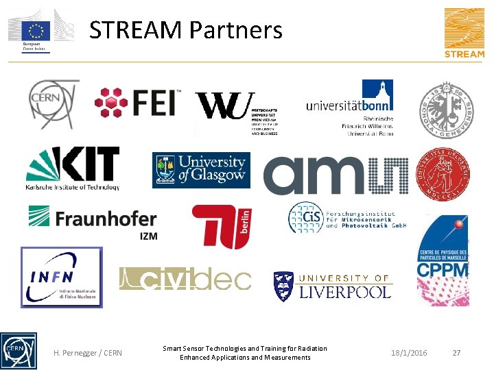
STREAM Partners H. Pernegger / CERN Smart Sensor Technologies and Training for Radiation Enhanced Applications and Measurements 18/1/2016 27

Your STREAM Team • Network Coordination – H. Pernegger <Heinz. Pernegger@cern. ch> – M. Capeans <Mar. Capeans@cern. ch> • Administation – Seamus Hegarty <Seamus. Hegarty@cern. ch> – Cecile Granier <Cecile. Granier@cern. ch> – Hanna Poikela <hanna. juujarvi@cern. ch> • Legal Advice – Karen Ernst <karen. ernst@cern. ch> • Financial Planning – Florence Pesce <stream-finance-support@cern. ch> H. Pernegger / CERN Smart Sensor Technologies and Training for Radiation Enhanced Applications and Measurements 18/1/2016 28

STREAM Partners CERN: Contacts: H. Pernegger, M. Capeans, S. Hegarty, C. Granier, H. Poikela Bonn: Contact: N. Wermes FEI: Contact: L. Mele, F. de Jong H. Pernegger / CERN Smart Sensor Technologies and Training for Radiation Enhanced Applications and Measurements 18/1/2016 29

STREAM Partners Fraunhofer IZM: Contacts: T. Fritzsch, O. Ehrmann KIT: Contact: I. Peric WU Wien Contact: P. Keinz Glasgow Contact: C. Buttar H. Pernegger / CERN Smart Sensor Technologies and Training for Radiation Enhanced Applications and Measurements 18/1/2016 30

STREAM partners Geneva: Contacts: G. Iacobucci, S. Gonzalez Sevilla Ci. S: Contact: R. Roder, T. Wittig ams: Contact: I. Jonak-Auer CPPM: Contacts: A. Rozanov, M. Barbero H. Pernegger / CERN Smart Sensor Technologies and Training for Radiation Enhanced Applications and Measurements 18/1/2016 31

STREAM Partners Liverpool: Contacts: G. Casse TU Berlin: Contact: R. Thewes INFN Milano: Contact: C. Meroni CIVIDEC: Contact: E. Griesmayer Oslo: Contact: H. Sandaker, S. Stapnes, O. Rohne H. Pernegger / CERN Smart Sensor Technologies and Training for Radiation Enhanced Applications and Measurements 18/1/2016 32

Today’s Kick-off meeting • Today’s kick-off meeting is the first occasion to meet each other and exchange ideas • The meeting will give an overview of STREAM’s research work packages and administrative procedures for the MC ITN. – – – ITN management and recruitment (S. Hegarty) Financial management (G. Cavallo) STREAM Project Office & Outreach (H. Poikela) STREAM Training Program (M. Capeans) STREAM Research Program (work package leaders) 1 st STREAM Supervisory Board H. Pernegger / CERN Smart Sensor Technologies and Training for Radiation Enhanced Applications and Measurements 18/1/2016 33

I would like to welcome you to the STREAM project and wish you a fruitful collaboration on the STREAM Marie Skłodowska. Curie Innovative Training Network! H. Pernegger / CERN Smart Sensor Technologies and Training for Radiation Enhanced Applications and Measurements 18/1/2016 34